# INA1x8 High-Side Measurement Current Shunt Monitor

## 1 Features

1• Complete Unipolar High-Side Current Measurement Circuit

• Wide Supply and Common-Mode Range

• INA138: 2.7 V to 36 V

• INA168: 2.7 V to 60 V

• Independent Supply and Input Common-Mode Voltages

• Single Resistor Gain Set

• Low Quiescent Current (25 µA Typical)

• Wide Temperature Range: –40°C to +125°C

• 5-Pin SOT-23 Package

## 2 Applications

• Current Shunt Measurement:

– Telephone, Computers

• Portable and Battery-Backup Systems

• Battery Chargers

• Power Management

• Cell Phones

• Precision Current Source

## 3 Description

The INA138 and INA168 (INA1x8) are high-side, unipolar, current shunt monitors. Wide input commonmode voltage range, low quiescent current, and tiny SOT-23 packaging enable use in a variety of applications.

Input common-mode and power-supply voltages are independent and can range from 2.7 V to 36 V for the INA138 and 2.7 V to 60 V for the INA168. Quiescent current is only 25 µA, which permits connecting the power supply to either side of the current measurement shunt with minimal error.

The device converts a differential input voltage to a current output. This current is converted back to a voltage with an external load resistor that sets any gain from 1 to over 100. Although designed for current shunt measurement, the circuit invites creative applications in measurement and level shifting.

Both the INA138 and INA168 are available in SOT23- 5 and are specified for the $\scriptscriptstyle - 4 0 ^ { \circ } \mathsf { C }$ to 125°C temperature range.

Device Information<sup>(1)</sup>

<table><tr><td>PART NUMBER</td><td>PACKAGE</td><td>BODY SIZE (NOM)</td></tr><tr><td>INA138</td><td rowspan="2">SOT-23 (5)</td><td rowspan="2">2.90 mm × 1.60 mm</td></tr><tr><td>INA168</td></tr></table>

(1) For all available packages, see the package option addendum at the end of the datasheet.

Typical Application Circuit  
![](https://www.embedr.app/api/datasheets/ds_08833a727e66254e6252/asset?path=images%2F5a2b3ad1d20d80a35f4d0fa51ebc4d64ad933bf0acee3f911ddc59fc2e8826d7.jpg)  
Copyright © 1999, Texas Instruments Incorporated

## Table of Contents

1 Features.... 1
2 Applications.... 1
3 Description.... 1
4 Revision History.... 2
5 Pin Configuration and Functions.... 3
6 Specifications.... 4
6.1 Absolute Maximum Ratings.... 4
6.2 ESD Ratings.... 4
6.3 Recommended Operating Conditions.... 4
6.4 Thermal Information.... 5
6.5 Electrical Characteristics.... 5
6.6 Typical Characteristics.... 6
7 Detailed Description.... 8
7.1 Overview.... 8
7.2 Functional Block Diagram.... 8
7.3 Feature Description.... 9
7.4 Device Functional Modes.... 9

8 Application and Implementation.... 10
8.1 Application Information.... 10
8.2 Typical Applications.... 11
9 Power Supply Recommendations.... 18
10 Layout.... 18
10.1 Layout Guidelines.... 18
10.2 Layout Example.... 18
11 Device and Documentation Support.... 19
11.1 Documentation Support.... 19
11.2 Related Links.... 19
11.3 Receiving Notification of Documentation Updates.... 19
11.4 Community Resources.... 19
11.5 Trademarks.... 19
11.6 Electrostatic Discharge Caution.... 19
11.7 Glossary.... 19
12 Mechanical, Packaging, and Orderable Information.... 20

## 4 Revision History

NOTE: Page numbers for previous revisions may differ from page numbers in the current version.

Changes from Revision D (December 2014) to Revision E Page
- Added reference design link to navigation bar at the top of the front page .... 1
- Changed body size from 18.00 mm × 18.00 mm to 2.90 mm × 1.60 mm in Device Information table.... 1
- Changed pin numbers in pin functions table to match pin configuration figure.... 3
- Changed Absolute Maximum Ratings table for clarity; no values were changed .... 4
- Changed Recommended Operating Conditions table; moved some content from Electrical Characteristics table, but no values changed .... 4
- Changed all values in Thermal Information table.... 5
- Changed Electrical Characteristics table; reformatted for clarity; moved some content to Recommended Operating Conditions table, and deleted duplicate content.... 5
- Changed common-mode rejection test conditions to better highlight each device in Electrical Characteristics table .... 5
- Changed offset voltage vs temperature to offset voltage drift in Electrical Characteristics table.... 5
- Changed offset voltage vs power supply test conditions to better highlight each device in Electrical Characteristics table . 5
- Changed reference in text from Figure 10 to Figure 11 in last paragraph of Selecting the Shunt Resistor and $R_L$ section 12

## Changes from Revision C (November 2005) to Revision D

Added ESD Ratings table, Feature Description section, Device Functional Modes, Application and Implementation section, Power Supply Recommendations section, Layout section, Device and Documentation Support section, and Mechanical, Packaging, and Orderable Information section. .

## 5 Pin Configuration and Functions

![](https://www.embedr.app/api/datasheets/ds_08833a727e66254e6252/asset?path=images%2Fb618c80ec40315d058ce7a1b318f27fce7af5ba350181b307b45596330cfd20c.jpg)

Pin Functions

<table><tr><td colspan="2">PIN</td><td rowspan="2">I/O</td><td rowspan="2">DESCRIPTION</td></tr><tr><td>NO.</td><td>NAME</td></tr><tr><td>1</td><td>OUT</td><td>O</td><td>Output current</td></tr><tr><td>2</td><td>GND</td><td>—</td><td>Ground</td></tr><tr><td>3</td><td>VIN+</td><td>I</td><td>Positive input voltage</td></tr><tr><td>4</td><td>VIN-</td><td>I</td><td>Negative input voltage</td></tr><tr><td>5</td><td>V+</td><td>I</td><td>Power supply voltage</td></tr></table>

## 6 Specifications

## 6.1 Absolute Maximum Ratings

over operating free-air temperature range (unless otherwise noted) <sup>(1)</sup>

<table><tr><td colspan="4"></td><td>MIN</td><td>MAX</td><td>UNIT</td></tr><tr><td rowspan="7">Voltage</td><td rowspan="2">Supply, V+</td><td colspan="2">INA138</td><td>-0.3</td><td>60</td><td rowspan="7">V</td></tr><tr><td colspan="2">INA168</td><td>-0.3</td><td>75</td></tr><tr><td rowspan="4">Analog input,  $V_{IN+}$ ,  $V_{IN-}$ </td><td rowspan="2">INA138</td><td>Common mode(2)</td><td>-0.3</td><td>60</td></tr><tr><td>Sense voltage,  $V_{SENSE} = (V_{IN+} - V_{IN-})$ </td><td>-40</td><td>2</td></tr><tr><td rowspan="2">INA168</td><td>Common mode(2)</td><td>-0.3</td><td>75</td></tr><tr><td>Sense voltage,  $V_{SENSE} = (V_{IN+} - V_{IN-})$ </td><td>-40</td><td>2</td></tr><tr><td colspan="3">Analog output, OUT pin(2)</td><td>-0.3</td><td>40</td></tr><tr><td>Current</td><td colspan="3">Input current into any pin</td><td></td><td>10</td><td>mA</td></tr><tr><td rowspan="3">Temperature</td><td colspan="3">Operating,  $T_A$ </td><td>-55</td><td>150</td><td rowspan="3">°C</td></tr><tr><td colspan="3">Junction,  $T_J$ </td><td></td><td>150</td></tr><tr><td colspan="3">Storage,  $T_{stg}$ </td><td>-65</td><td>150</td></tr></table>

(1) Stresses beyond those listed under Absolute Maximum Ratings may cause permanent damage to the device. These are stress ratings only, which do not imply functional operation of the device at these or any other conditions beyond those indicated under Recommended Operating Conditions. Exposure to absolute-maximum-rated conditions for extended periods may affect device reliability.

(2) The input voltage at any pin may exceed the voltage shown if the current at that pin is limited to 10 mA.

## 6.2 ESD Ratings

<table><tr><td colspan="2"></td><td>VALUE</td><td>UNIT</td></tr><tr><td rowspan="2"> $V_{(ESD)}$  Electrostatic discharge</td><td>Human-body model (HBM), per ANSI/ESDA/JEDEC JS-001 $^{(1)}$ </td><td>±1000</td><td rowspan="2">V</td></tr><tr><td>Charged-device model (CDM), per JEDEC specification JESD22-C101 $^{(2)}$ </td><td>±500</td></tr></table>

(1) JEDEC document JEP155 states that 500-V HBM allows safe manufacturing with a standard ESD control process. (2) JEDEC document JEP157 states that 250-V CDM allows safe manufacturing with a standard ESD control process.

## 6.3 Recommended Operating Conditions

over operating free-air temperature range (unless otherwise noted)

<table><tr><td colspan="2"></td><td>MIN</td><td>NOM</td><td>MAX</td><td>UNIT</td></tr><tr><td colspan="6">INA138</td></tr><tr><td>V+</td><td>Supply voltage</td><td>2.7</td><td>5</td><td>36</td><td>V</td></tr><tr><td> $V_{SENSE}$ </td><td>Full-scale sense voltage ( $V_{IN+}-V_{IN-}$ )</td><td></td><td>100</td><td>500</td><td>mV</td></tr><tr><td></td><td>Common-mode voltage</td><td>2.7</td><td>12</td><td>36</td><td>V</td></tr><tr><td> $T_A$ </td><td>Operating temperature</td><td>-40</td><td>25</td><td>125</td><td>°C</td></tr><tr><td colspan="6">INA168</td></tr><tr><td>V+</td><td>Supply voltage</td><td>2.7</td><td>5</td><td>60</td><td>V</td></tr><tr><td> $V_{SENSE}$ </td><td>Full-scale sense voltage ( $V_{IN+}-V_{IN-}$ )</td><td></td><td>100</td><td>500</td><td>mV</td></tr><tr><td></td><td>Common-mode voltage</td><td>2.7</td><td>12</td><td>60</td><td>V</td></tr><tr><td> $T_A$ </td><td>Operating temperature</td><td>-40</td><td>25</td><td>125</td><td>°C</td></tr></table>

## 6.4 Thermal Information

<table><tr><td rowspan="3" colspan="2">THERMAL METRIC(1)</td><td>INA1x8</td><td rowspan="3">UNIT</td></tr><tr><td>DBV</td></tr><tr><td>5 PINS</td></tr><tr><td> $R_{\theta JA}$ </td><td>Junction-to-ambient thermal resistance</td><td>168.3</td><td>°C/W</td></tr><tr><td> $R_{\theta JC(top)}$ </td><td>Junction-to-case (top) thermal resistance</td><td>73.8</td><td>°C/W</td></tr><tr><td> $R_{\theta JB}$ </td><td>Junction-to-board thermal resistance</td><td>28.1</td><td>°C/W</td></tr><tr><td> $\psi_{JT}$ </td><td>Junction-to-top characterization parameter</td><td>2.5</td><td>°C/W</td></tr><tr><td> $\psi_{JB}$ </td><td>Junction-to-board characterization parameter</td><td>27.6</td><td>°C/W</td></tr></table>

(1) For more information about traditional and new thermal metrics, see the Semiconductor and IC Package Thermal Metrics application report.

## 6.5 Electrical Characteristics

all other characteristics at $T _ { \mathrm { A } } = + 2 5 ^ { \circ } \mathrm { C } , \mathrm { V } _ { \mathrm { S } } = 5 \mathrm { V } , \mathrm { V } _ { \vert \mathrm { N } + } = 1 2 \mathrm { V } ,$ and $\mathsf { R } _ { \mathsf { O U T } } = 1 2 5$ kΩ (unless otherwise noted)

<table><tr><td rowspan="2">PARAMETER</td><td rowspan="2" colspan="2">TEST CONDITIONS</td><td colspan="3">INA1x8</td><td rowspan="2">UNIT</td></tr><tr><td>MIN</td><td>TYP</td><td>MAX</td></tr><tr><td colspan="7">INPUT</td></tr><tr><td rowspan="2">Common-mode rejection</td><td rowspan="2"> $V_{SENSE}$ =50 mV</td><td>INA138,  $V_{IN+}$ =2.7 V to 36 V</td><td>100</td><td>120</td><td></td><td rowspan="2">dB</td></tr><tr><td>INA168,  $V_{IN+}$ =2.7 V to 60 V</td><td>100</td><td>120</td><td></td></tr><tr><td rowspan="2">Offset  $voltage^{(1)}$ </td><td colspan="2"> $T_A$ =25°C</td><td colspan="2">±0.2</td><td>±1</td><td rowspan="2">mV</td></tr><tr><td colspan="2"> $T_A$ =-40°C to +125°C</td><td colspan="3">±2</td></tr><tr><td>Offset  $voltage drift^{(1)}$ </td><td colspan="2"> $T_A$ =-40°C to +125°C</td><td colspan="3">1</td><td>μV/°C</td></tr><tr><td rowspan="2">Offset voltage vs power supply, V+</td><td rowspan="2"> $V_{SENSE}$ =50 mV</td><td>INA138, V+=2.7 V to 36 V</td><td colspan="2">0.1</td><td>10</td><td rowspan="2">μV/V</td></tr><tr><td>INA168, V+=2.7 V to 60 V</td><td colspan="2">0.1</td><td>10</td></tr><tr><td rowspan="2">Input bias current</td><td colspan="2"> $T_A$ =25°C</td><td colspan="3">2</td><td rowspan="2">μA</td></tr><tr><td colspan="2"> $T_A$ =-40°C to +125°C, INA138</td><td colspan="3">10</td></tr><tr><td colspan="7">OUTPUT</td></tr><tr><td rowspan="2">Transconductance</td><td colspan="2"> $V_{SENSE}$ =10 mV to 150 mV,  $T_A$ =25°C</td><td>198</td><td>200</td><td>202</td><td>μA/V</td></tr><tr><td colspan="2"> $V_{SENSE}$ =100 mV,  $T_A$ =-40°C to +125°C</td><td>196</td><td></td><td>204</td><td>μA/V</td></tr><tr><td>Transconductance drift</td><td colspan="2"> $T_A$ =-40°C to +125°C</td><td colspan="3">10</td><td>nA/°C</td></tr><tr><td>Nonlinearity error</td><td colspan="2"> $V_{SENSE}$ =10 mV to 150 mV</td><td colspan="2">±0.01%</td><td>±0.1%</td><td></td></tr><tr><td rowspan="2">Total output error</td><td rowspan="2"> $V_{SENSE}$ =100 mV</td><td> $T_A$ =25°C</td><td colspan="2">±0.5%</td><td>±2%</td><td></td></tr><tr><td> $T_A$ =-40°C to +125°C</td><td colspan="3">±2.5%</td><td></td></tr><tr><td>Output impedance</td><td colspan="2"></td><td colspan="3">1 || 5</td><td>GΩ || pF</td></tr><tr><td rowspan="2">Voltage output swing</td><td colspan="2">To power supply voltage, V+</td><td colspan="2">(V+) - 0.8</td><td>(V+) - 1.0</td><td>V</td></tr><tr><td colspan="2">To common-mode voltage,  $V_{CM}$ </td><td colspan="2"> $V_{CM}$ -0.5</td><td> $V_{CM}$ -0.8</td><td>V</td></tr><tr><td colspan="7">FREQUENCY RESPONSE</td></tr><tr><td rowspan="2">Bandwidth</td><td colspan="2"> $R_{OUT}$ =5 kΩ</td><td colspan="3">800</td><td>kHz</td></tr><tr><td colspan="2"> $R_{OUT}$ =125 kΩ</td><td colspan="3">32</td><td>kHz</td></tr><tr><td rowspan="2">Settling time</td><td rowspan="2">To 0.1%</td><td>5-V step,  $R_{OUT}$ =5 kΩ</td><td colspan="3">1.8</td><td>μs</td></tr><tr><td>5-V step,  $R_{OUT}$ =125 kΩ</td><td colspan="3">30</td><td>μs</td></tr><tr><td colspan="7">NOISE</td></tr><tr><td>Output-current noise density</td><td colspan="2"></td><td colspan="3">9</td><td>pA/ $\sqrt{Hz}$ </td></tr><tr><td>Total output-current noise</td><td colspan="2">BW=100 kHz</td><td colspan="3">3</td><td>nA RMS</td></tr><tr><td colspan="7">POWER SUPPLY</td></tr><tr><td rowspan="2">Quiescent current</td><td rowspan="2"> $V_{SENSE}$ =0 V, $I_O$ =0 mA</td><td> $T_A$ =25°C</td><td colspan="2">25</td><td>45</td><td>μA</td></tr><tr><td> $T_A$ =-40°C to +125°C</td><td colspan="3">60</td><td>μA</td></tr></table>

(1) Defined as the amount of input voltage, $\mathsf { V } _ { \mathsf { S E N S E } } ,$ to drive the output to zero.

## 6.6 Typical Characteristics

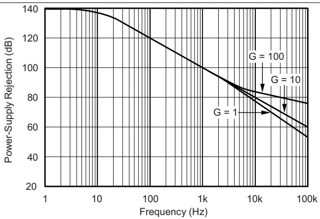
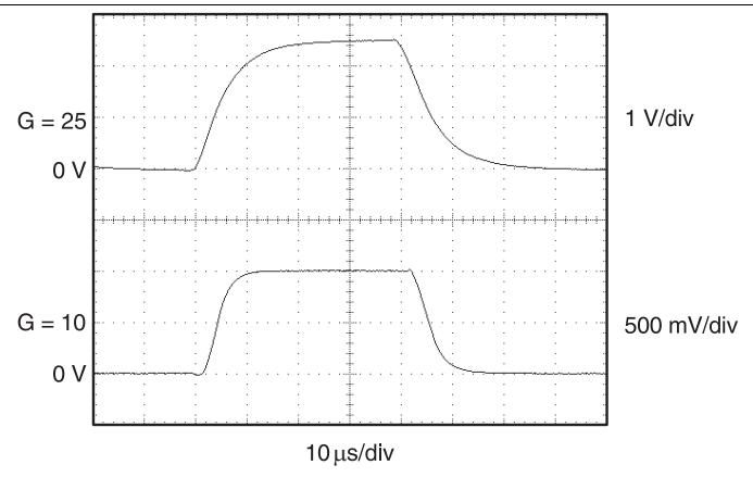
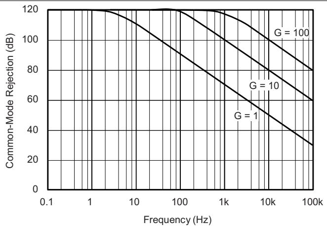
At ${ \sf T } _ { \sf A } = + 2 5 ^ { \circ } { \sf C }$ , V+ = 5 V, $\mathsf { V } _ { | \mathsf { N } + } = 1 2 \mathsf { V } ,$ and $\mathsf { R } _ { \mathsf { L } } = 1 2 5 \mathsf { k } \Omega ,$ unless otherwise noted.
![](https://www.embedr.app/api/datasheets/ds_08833a727e66254e6252/asset?path=images%2Facf0714c8be04992834f04188bd463fddf5a3de9e325f5a065a58b740ee859a5.jpg)

![](https://www.embedr.app/api/datasheets/ds_08833a727e66254e6252/asset?path=images%2F2af9b587343c793bb5271b2fba5d8164c3b37622f0db5de919399cfefee1e506.jpg)

Figure 1. Gain vs Frequency  
![](https://www.embedr.app/api/datasheets/ds_08833a727e66254e6252/asset?path=images%2F59652c07795de3d0e6c80f4bd1c5715fefff743279e2c692cedecb660947be31.jpg)

Figure 2. Common-Mode Rejection vs Frequency  
![](https://www.embedr.app/api/datasheets/ds_08833a727e66254e6252/asset?path=images%2F3778d43f38c5543f7e558786bd33659f6c0c9e8479f1b98b6fb00261aed9977d.jpg)

Figure 3. Power-Supply Rejection vs Frequency  
![](https://www.embedr.app/api/datasheets/ds_08833a727e66254e6252/asset?path=images%2Fc0d91d04c4e0f0748288c2a62164394f5b5effae0fd9cb2fab624df32f5a89f7.jpg)  
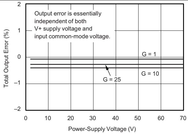
Figure 5. Total Output Error vs Power-Supply Voltage

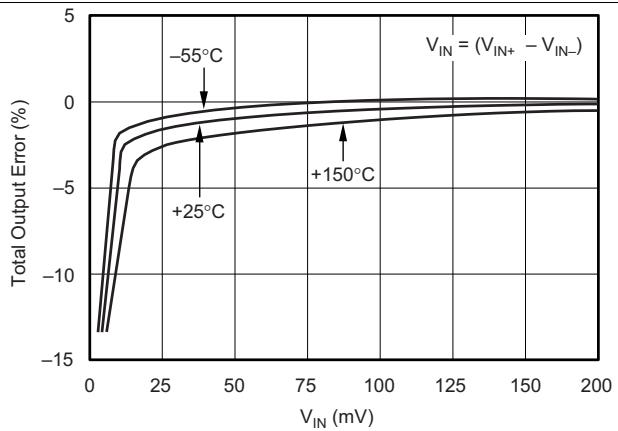
Figure 4. Total Output Error vs $\mathsf { v } _ { \mathsf { I N } }$  
![](https://www.embedr.app/api/datasheets/ds_08833a727e66254e6252/asset?path=images%2Fcfd4cdd6378d571121311d9f760799eecc348e7a1895f0cd8bd7e70e0fab32be.jpg)  
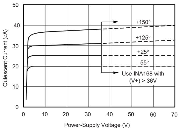
Figure 6. Quiescent Current vs Power-Supply Voltage

## Typical Characteristics (continued)

At ${ \sf T } _ { \sf A } = + 2 5 ^ { \circ } { \sf C }$ , V+ = 5 V, $\mathsf { V } _ { | \mathsf { N } + } = 1 2 \mathsf { V } ,$ and $\mathsf { R } _ { \mathsf { L } } = 1 2 5$ kΩ, unless otherwise noted.  
![](https://www.embedr.app/api/datasheets/ds_08833a727e66254e6252/asset?path=images%2F69a0a1f396cc099548dbe1d32d24e56e99f5b70ed00950f916fb525152d953a2.jpg)  
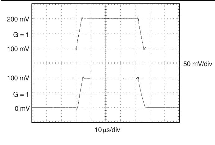
Figure 7. Step Response

![](https://www.embedr.app/api/datasheets/ds_08833a727e66254e6252/asset?path=images%2Facbc71b5c0ec247ffa80f5ac6770d16cf54e1f311afaa071a43ee113ddbeeede.jpg)  
Figure 8. Step Response

## 7 Detailed Description

## 7.1 Overview

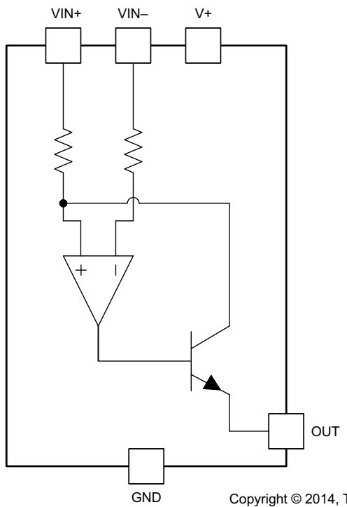
The INA138 and INA168 devices (INA1x8) are comprised of a high voltage, precision operational amplifier, precision thin film resistors trimmed in production to an absolute tolerance and a low noise output transistor. The INA1x8 devices can be powered from a single power supply and their input voltages can exceed the power supply voltage. The INA1x8 devices are ideal for measuring small differential voltages, such as those generated across a shunt resistor, in the presence of large common-mode voltages. Refer to Functional Block Diagram which illustrates the functional components within both INA1x8 devices.

## 7.2 Functional Block Diagram
![](https://www.embedr.app/api/datasheets/ds_08833a727e66254e6252/asset?path=images%2F0536e4de29599d1913aba1a7361520bd46155011d85b1b434a74742b72c1eb35.jpg)  
Copyright © 2014, Texas Instruments Incorporated

## 7.3 Feature Description

## 7.3.1 Output Voltage Range

The output of the INA1x8 device is a current that is converted to a voltage by the load resistor, $\mathsf { R } _ { \mathsf { L } }$ . The output current remains accurate within the compliance voltage range of the output circuitry. The shunt voltage and the input common-mode and power-supply voltages limit the maximum possible output swing. The maximum output voltage $\left( \mathsf { V } _ { \mathsf { o u t \ m a x } } \right)$ compliance is limited by either Equation 1 or Equation $^ { 2 , }$ whichever is lower:

$$
V _ {\text { out   max }} = (V +) - 0. 7 \mathrm{V} - (V _ {\mathrm{IN+}} - V _ {\mathrm{IN-}})\tag{1}
$$

or

$$
V _ {\text {out max}} = V _ {\text {IN-}} - 0. 5 \mathrm{V}\tag{2}
$$

## 7.3.2 Bandwidth

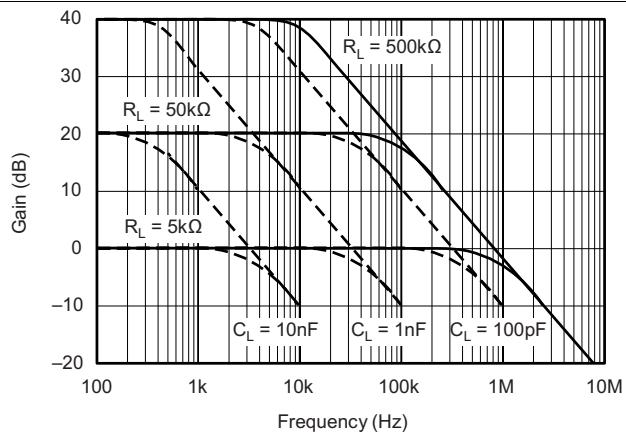
Measurement bandwidth is affected by the value of the load resistor, ${ \sf R } _ { \sf L }$ . High gain produced by high values of $\mathsf { R } _ { \mathsf { L } }$ will yield a narrower measurement bandwidth (see Typical Characteristics). For widest possible bandwidth, keep the capacitive load on the output to a minimum. Reduction in bandwidth due to capacitive load is shown in the Typical Characteristics.

If bandwidth limiting (filtering) is desired, a capacitor can be added to the output (see Figure 12). This will not cause instability.

## 7.4 Device Functional Modes

For proper operation the INA1x8 devices must operate within their specified limits. Operating either device outside of their specified power supply voltage range or their specified common-mode range will result in unexpected behavior and is not recommended. Additionally operating the output beyond their specified limits with respect to power supply voltage and input common-mode voltage will also produce unexpected results. Refer to Electrical Characteristics for the device specifications.

## 8 Application and Implementation

## NOTE

Information in the following applications sections is not part of the TI component specification, and TI does not warrant its accuracy or completeness. TI’s customers are responsible for determining suitability of components for their purposes. Customers should validate and test their design implementation to confirm system functionality.

## 8.1 Application Information

## 8.1.1 Operation

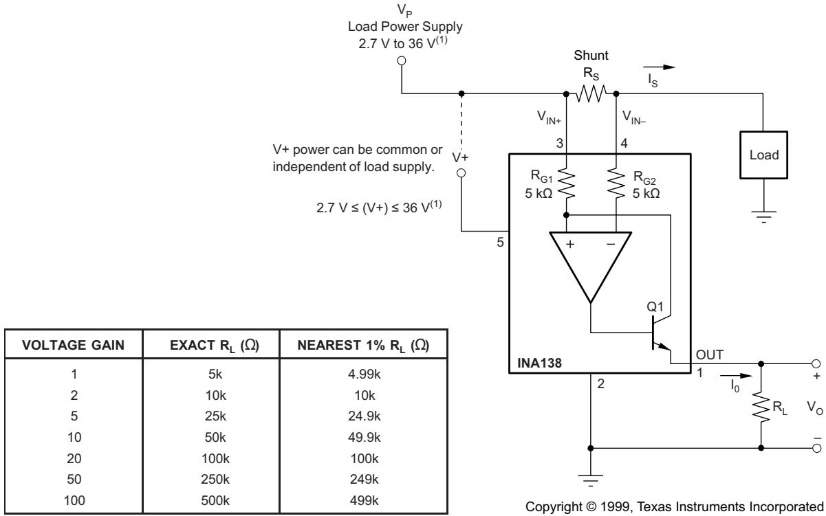
Figure 9 illustrates the basic circuit diagram for both the INA138 and INA168 devices. Load current $\mathsf { I } _ { \mathsf { S } }$ is drawn from supply ${ \sf V } _ { \sf S }$ through shunt resistor $\mathsf { R } _ { \mathsf { S } }$ . The voltage drop in shunt resistor $\mathsf { V } _ { \mathsf { S } }$ is forced across $\mathsf { R } _ { \mathsf { G } 1 }$ by the internal op amp, causing current to flow into the collector of Q1. External resistor $\mathsf { R } _ { \mathsf { L } }$ converts the output current to a voltage, $\mathsf { V } _ { \mathsf { O U T } } ,$ at the OUT pin. The transfer function for the INA138 device is:

$$
I _ {O} = g _ {m} \left(V _ {I N +} - V _ {I N -}\right)\tag{3}
$$

where ${ \mathfrak { g } } _ { \mathfrak { m } } = 2 0 0 \mu { \mu \mathrm { A } } / \nu .$

In the circuit of Figure 9, the input voltage, $( \mathsf { V } _ { | \mathsf { N } + } - \mathsf { V } _ { | \mathsf { N } - } )$ , is equal to $\mathsf { I } _ { \mathsf { S } } \times \mathsf { R } _ { \mathsf { S } }$ and the output voltage, $\mathsf { V } _ { \mathsf { O U T } } ,$ is equal to ${ \mathsf I } _ { 0 } \times { \mathsf R } _ { \mathsf L }$ . The transconductance, $\mathsf { { g } } _ { \mathsf { m } } ,$ of the INA138 device is 200 µA/V. The complete transfer function for the current measurement amplifier in this application is:

$$
V _ {\text {OUT}} = (I _ {S}) (R _ {S}) (2 0 0 \mu \text {A} / \text {V}) (R _ {L})\tag{4}
$$

The maximum differential input voltage for accurate measurements is 0.5 V, which produces a 100-µA output current. A differential input voltage of up to 2 V will not cause damage. Differential measurements (pins 3 and 4) must be unipolar with a more-positive voltage applied to pin 3. If a more-negative voltage is applied to pin 3, the output current, ${ \mathsf { I } } _ { 0 } ,$ will be zero, but it will not cause damage.
![](https://www.embedr.app/api/datasheets/ds_08833a727e66254e6252/asset?path=images%2F7f811af14b3720607b6453f01c656b529e77aa6cf4e4a09760d9d534783cc8f6.jpg)

<table><tr><td>VOLTAGE GAIN</td><td>EXACT RL(Ω)</td><td>NEAREST 1% RL(Ω)</td></tr><tr><td>1</td><td>5k</td><td>4.99k</td></tr><tr><td>2</td><td>10k</td><td>10k</td></tr><tr><td>5</td><td>25k</td><td>24.9k</td></tr><tr><td>10</td><td>50k</td><td>49.9k</td></tr><tr><td>20</td><td>100k</td><td>100k</td></tr><tr><td>50</td><td>250k</td><td>249k</td></tr><tr><td>100</td><td>500k</td><td>499k</td></tr></table>

(1) Maximum $\mathsf { V } _ { \mathsf { P } }$ and V+ voltage is 60 V with INA168.

Figure 9. Basic Circuit Connections

## 8.2 Typical Applications

The INA1x8 devices are designed for current shunt measurement circuits, as shown in Figure 9, but basic device function is useful in a wide range of circuitry. A creative engineer will find many unforeseen uses in measurement and level-shifting circuits. A few ideas are illustrated in Figure 10 through Figure 18.

## 8.2.1 Buffering Output to Drive an ADC

![](https://www.embedr.app/api/datasheets/ds_08833a727e66254e6252/asset?path=images%2Ff3365519d0f49d51052492d9b97586f4e29352bcfb6813dc111d6998c42685f6.jpg)  
Figure 10. Buffering Output to Drive an ADC

## 8.2.1.1 Design Requirements

Digitize the output of the INA1x8 devices using a 1-MSPS analog-to-digital converter (ADC).

## 8.2.1.2 Detailed Design Procedure

## 8.2.1.2.1 Selecting the Shunt Resistor and $\mathsf { R } _ { \mathsf { L } }$

In Figure 9 the value chosen for the shunt resistor depends on the application and is a compromise between small-signal accuracy and maximum permissible voltage loss in the measurement line. High values of shunt resistor provide better accuracy at lower currents by minimizing the effects of offset, while low values of shunt resistor minimize voltage loss in the supply line. For most applications, best performance is attained with a shunt resistor value that provides a full-scale shunt voltage range of 50 mV to 100 mV. Maximum input voltage for accurate measurements is 500 mV.

The load resistor, $\mathsf { R } _ { \mathsf { L } } ,$ is chosen to provide the desired full-scale output voltage. The output impedance of the INA1x8 OUT terminal is very high which permits using values of ${ \sf R } _ { \sf L }$ up to 500 kΩ with excellent accuracy. The input impedance of any additional circuitry at the output should be much higher than the value of $\mathsf { R } _ { \mathsf { L } }$ to avoid degrading accuracy.

Some analog-to-digital converters (ADCs) have input impedances that significantly affect measurement gain. The input impedance of the ADC can be included as part of the effective ${ \sf R } _ { \sf L }$ if its input can be modeled as a resistor to ground. Alternatively, an op amp can be used to buffer the ADC input. The INA1x8 are current output devices, and as such have an inherently large output impedance. The output currents from the amplifier are converted to an output voltage via the load resistor, $\mathsf { R } _ { \mathsf { L } }$ , connected from the amplifier output to ground. The ratio of the load resistor value to that of the internal resistor value determines the voltage gain of the system.

In many applications digitizing the output of the INA1x8 device is required, and can be accomplished by connecting the output of the amplifier to an ADC. It is very common for an ADC to have a dynamic input impedance. If the INA1x8 output is connected directly to an ADC input, the input impedance of the ADC is effectively connected in parallel with the gain setting resistor $\mathsf { R } _ { \mathsf { L } } .$ . This parallel impedance combination will affect the gain of the system and the impact on the gain is difficult to estimate accurately. A simple solution that eliminates the paralleling of impedances, simplifying the gain of the circuit is to place a buffer amplifier, such as the OPA340, between the output of the INA138 or INA168 device and the input to the ADC.

## Typical Applications (continued)

Figure 10 illustrates this concept. Notice that a low pass filter is placed between the OPA340 output and the input to the ADC. The filter capacitor is required to provide any instantaneous demand for current required by the input stage of the ADC. The filter resistor is required to isolate the OPA340 output from the filter capacitor to maintain circuit stability. The values for the filter components will vary according to the operational amplifier used for the buffer and the particular ADC selected. More information can be found regarding the design of the low pass filter in the TI Precision Design , 16 bit 1MSPS Data Acquisition Reference Design for Single-Ended Multiplexed Applications (TIPD173).

Figure 11 shows the expected results when driving an analog-to-digital converter at 1MSPS with and without buffering the INA1x8 output. Without the buffer, the high impedance of the INA1x8 reacts with the input capacitance and sample and hold (S/H) capacitance of the ADC, and does not allow the S/H to reach the correct final value before it is reset and the next conversion starts. Adding the buffer amplifier significantly reduces the output impedance driving the S/H and allows for higher conversion rates than can be achieved without adding the buffer.

## 8.2.1.3 Application Curve

![](https://www.embedr.app/api/datasheets/ds_08833a727e66254e6252/asset?path=images%2Fd012dc3d65fed56dfc57938a611f8cb85dc54d9078b6b6b9adcf5c100903fca0.jpg)  
Figure 11. Driving an ADC With and Without a Buffer

## Typical Applications (continued)

## 8.2.2 Output Filter

![](https://www.embedr.app/api/datasheets/ds_08833a727e66254e6252/asset?path=images%2F98214d20873e6243b023602058e640f9e61ab7da30464b19a62d7bbf641f2dd8.jpg)  
Figure 12. Output Filter

## 8.2.2.1 Design Requirements

Filter the output of the INA1x8 devices.

## 8.2.2.2 Detailed Design Procedure

A low-pass filter can be formed at the output of the INA1x8 devices simply by placing a capacitor of the desired value in parallel with the load resistor. First determine the value of the load resistor needed to achieve the desired gain. Refer to the table in Figure 9. Next, determine the capacitor value that will result in the desired cutoff frequency according to the equation shown in Figure 12. Figure 13 illustrates various combinations of gain settings (determined by R ) and filter capacitors.

## 8.2.2.3 Application Curve

![](https://www.embedr.app/api/datasheets/ds_08833a727e66254e6252/asset?path=images%2Fdee3b17d2aa5209d1958346d98becc217269515c6c76bcd600b8978d0a2d7ef9.jpg)  
Figure 13. Gain vs Frequency

## Typical Applications (continued)

## 8.2.3 Offsetting the Output Voltage

For many applications using only a single power supply it may be required to level shift the output voltage away from ground when there is no load current flowing in the shunt resistor. Level shifting the output of the INA1x8 devices is easily accomplished by one of two simple methods shown in Figure 14. The method on the left hand side of Figure 14 illustrates a simple voltage divider method. This method is useful for applications that require the output of the INA1x8 devices to remain centered with respect to the power supply at zero load current through the shunt resistor. Using this method the gain is determine by the parallel combination of $\mathsf { R } _ { 1 }$ and ${ \sf R } _ { 2 }$ while the output offset is determined by the voltage divider ratio $\mathsf { R } _ { 1 }$ and $\mathsf { R } _ { 2 } .$ For applications that may require a fixed value of output offset, independent of the power supply voltage, the current source method shown on the right-hand side of Figure 14 is recommended. With this method a REF200 constant current source is used to generate a constant output offset. Using his method the gain is determined by $\mathsf { R } _ { \mathsf { L } }$ and the offset is determined by the product of the value of the current source and ${ \mathsf { R } } _ { \mathsf { L } }$

![](https://www.embedr.app/api/datasheets/ds_08833a727e66254e6252/asset?path=images%2F47b01a808e77567b045e85079ecf9356ee84d16692438bb267cb8777da8dff1c.jpg)  
a) Using resistor divider.

![](https://www.embedr.app/api/datasheets/ds_08833a727e66254e6252/asset?path=images%2F53256a7661a4282fb19adb97fe8889dc05f46213f18a008079d97d088ef3dfc8.jpg)  
b) Using current source.  
Figure 14. Offsetting the Output Voltage

## Typical Applications (continued)

## 8.2.4 Bipolar Current Measurement

The INA1x8 devices can be configured as shown in Figure 15 in applications where measuring current bidirectionally is required. Two INA devices are required connecting their inputs across the shunt resistor as shown in Figure 15. A comparator, such as the TLV3201, is used to detect the polarity of the load current. The magnitude of the load current is monitored across the resistor connected between ground and the connection labeled Output. In this example the 100-kΩ resistor results in a gain of 20 V/V. The 10-kΩ resistors connected in series with the INA1x8 output current are used to develop a voltage across the comparator inputs. Two diodes are required to prevent current flow into the INA1x8 output, as only one device at a time is providing current to the Output connection of the circuit. The circuit functionality is illustrated in Figure 16.

![](https://www.embedr.app/api/datasheets/ds_08833a727e66254e6252/asset?path=images%2F2c94b2c43f06040514849f743906c382d2274ea0572a43e19def7972c995beba.jpg)  
Figure 15. Bipolar Current Measurement

## Typical Applications (continued)

![](https://www.embedr.app/api/datasheets/ds_08833a727e66254e6252/asset?path=images%2Fe9584d616cd266c4d0807385a0158a7e14aa03e3216f68ed29afd21244ea97ed.jpg)  
Figure 16. Bipolar Current Measurements Results (arbitrary scale)

## 8.2.5 Bipolar Current Measurement Using Differential Input of ADC

The INA1x8 devices can be used with an ADC such as the ADS7870 programmed for differential mode operation. Figure 17 illustrates this configuration. In this configuration the use of two INAs allows for bidirectional current measurement. Depending upon the polarity of the current, one of the INAs provides an output voltage, while the other output is zero. In this way the ADC reads the polarity of current directly, without the need for additional circuitry.

![](https://www.embedr.app/api/datasheets/ds_08833a727e66254e6252/asset?path=images%2Fbfc8ab2b2f9e125de6af0e51cf8e183b64220188e34ca3d194c992450e4b4a33.jpg)  
Figure 17. Bipolar Current Measurement Using Differential Input of ADC

## Typical Applications (continued)

## 8.2.6 Multiplexed Measurement Using Logic Signal for Power

Multiple loads can be measured as illustrated in Figure 18. In this configuration each INA1x8 device is powered by the digital I/O from the ADS7870. Multiplexing is achieved by switching on or off each the desired I/O.

![](https://www.embedr.app/api/datasheets/ds_08833a727e66254e6252/asset?path=images%2Fa0c3b59f64abc6144065efe4e9feafa6e7827214b9e7c0b25a62698407cc1d53.jpg)  
Figure 18. Multiplexed Measurement Using Logic Signal for Power

## 9 Power Supply Recommendations

The input circuitry of the INA138 can accurately measure beyond its power-supply voltage, V+. For example, the V+ power supply can be 5 V, whereas the load power supply voltage is up to 36 V (or 60 V with the INA168). The output voltage range of the OUT terminal, however, is limited by the lesser of the two voltages (see Output Voltage Range). A 0.1-µF capacitor is recommenced to be placed near the power supply pin on the INA138 or INA168. Additional capacitance may be required for applications with noisy power supply voltages.

## 10 Layout

## 10.1 Layout Guidelines

Figure 19 shows the basic connection of the INA138 device. The input pins, $\vee _ { { \mathsf { I N } } + }$ and $\vee _ { \mathsf { I N - } }$ , should be connected as closely as possible to the shunt resistor to minimize any resistance in series with the shunt resistance. The output resistor, $\mathsf { R } _ { \mathsf { L } }$ , is shown connected between pin 1 and ground. Best accuracy is achieved with the output voltage measured directly across $\mathsf { R } _ { \mathsf { L } }$ . This is especially important in high-current systems where load current could flow in the ground connections, affecting the measurement accuracy.

No power-supply bypass capacitors are required for stability of the INA138. However, applications with noisy or high-impedance power supplies may require decoupling capacitors to reject power-supply noise. Connect bypass capacitors close to the device pins.

## 10.2 Layout Example

VIA to Ground Plane  
![](https://www.embedr.app/api/datasheets/ds_08833a727e66254e6252/asset?path=images%2F2f7fe16932670d510df8db10da2d1f781a705988a8e70fc87719ab1905583d2a.jpg)  
Figure 19. Typical Layout Example

## 11 Device and Documentation Support

## 11.1 Documentation Support

## 11.1.1 Related Documentation

For related documentation see the following:

• 16 bit 1MSPS Data Acquisition Reference Design for Single-Ended Multiplexed Applications

• ADS7870 12-Bit ADC, MUX, PGA and Internal Reference Data Acquisition System

TLV3201, TLV3202 40-ns, microPOWER, Push-Pull Output Comparators

• REF200 Dual Current Source/Current Sink

## 11.2 Related Links

Table 1 lists quick access links. Categories include technical documents, support and community resources, tools and software, and quick access to sample or buy.

Table 1. Related Links

<table><tr><td>PARTS</td><td>PRODUCT FOLDER</td><td>SAMPLE &amp; BUY</td><td>TECHNICAL DOCUMENTS</td><td>TOOLS &amp; SOFTWARE</td><td>SUPPORT &amp; COMMUNITY</td></tr><tr><td>INA138</td><td>Click here</td><td>Click here</td><td>Click here</td><td>Click here</td><td>Click here</td></tr><tr><td>INA168</td><td>Click here</td><td>Click here</td><td>Click here</td><td>Click here</td><td>Click here</td></tr></table>

## 11.3 Receiving Notification of Documentation Updates

To receive notification of documentation updates, navigate to the device product folder on ti.com. In the upper right corner, click on Alert me to register and receive a weekly digest of any product information that has changed. For change details, review the revision history included in any revised document.

## 11.4 Community Resources

The following links connect to TI community resources. Linked contents are provided "AS IS" by the respective contributors. They do not constitute TI specifications and do not necessarily reflect TI's views; see TI's Terms of Use.

TI E2E™ Online Community TI's Engineer-to-Engineer (E2E) Community. Created to foster collaboration among engineers. At e2e.ti.com, you can ask questions, share knowledge, explore ideas and help solve problems with fellow engineers.

Design Support TI's Design Support Quickly find helpful E2E forums along with design support tools and contact information for technical support.

## 11.5 Trademarks

E2E is a trademark of Texas Instruments.

All other trademarks are the property of their respective owners.

## 11.6 Electrostatic Discharge Caution

![](https://www.embedr.app/api/datasheets/ds_08833a727e66254e6252/asset?path=images%2F891058107d7791c684db542e089564ef7841a755ebb2ed3210221c0247c55886.jpg)

This integrated circuit can be damaged by ESD. Texas Instruments recommends that all integrated circuits be handled with appropriate precautions. Failure to observe proper handling and installation procedures can cause damage.

ESD damage can range from subtle performance degradation to complete device failure. Precision integrated circuits may be more susceptible to damage because very small parametric changes could cause the device not to meet its published specifications.

## 11.7 Glossary

SLYZ022 — TI Glossary.

This glossary lists and explains terms, acronyms, and definitions.

## 12 Mechanical, Packaging, and Orderable Information

The following pages include mechanical, packaging, and orderable information. This information is the most current data available for the designated devices. This data is subject to change without notice and revision of this document. For browser-based versions of this data sheet, refer to the left-hand navigation.

## PACKAGING INFORMATION

<table><tr><td>Orderable part number</td><td>Status(1)</td><td>Material type(2)</td><td>Package | Pins</td><td>Package qty | Carrier</td><td>RoHS(3)</td><td>Lead finish/ Ball material(4)</td><td>MSL rating/ Peak reflow(5)</td><td>Op temp (°C)</td><td>Part marking(6)</td></tr><tr><td>INA138NA/250</td><td>Active</td><td>Production</td><td>SOT-23 (DBV) | 5</td><td>250 | SMALL T&amp;R</td><td>Yes</td><td>NIPDAU</td><td>Level-2-260C-1 YEAR</td><td>-40 to 125</td><td>B38</td></tr><tr><td>INA138NA/250.A</td><td>Active</td><td>Production</td><td>SOT-23 (DBV) | 5</td><td>250 | SMALL T&amp;R</td><td>Yes</td><td>NIPDAU</td><td>Level-2-260C-1 YEAR</td><td>-40 to 125</td><td>B38</td></tr><tr><td>INA138NA/3K</td><td>Active</td><td>Production</td><td>SOT-23 (DBV) | 5</td><td>3000 | LARGE T&amp;R</td><td>Yes</td><td>NIPDAU</td><td>Level-2-260C-1 YEAR</td><td>-40 to 125</td><td>B38</td></tr><tr><td>INA138NA/3K.A</td><td>Active</td><td>Production</td><td>SOT-23 (DBV) | 5</td><td>3000 | LARGE T&amp;R</td><td>Yes</td><td>NIPDAU</td><td>Level-2-260C-1 YEAR</td><td>-40 to 125</td><td>B38</td></tr><tr><td>INA168NA/250</td><td>Active</td><td>Production</td><td>SOT-23 (DBV) | 5</td><td>250 | SMALL T&amp;R</td><td>Yes</td><td>NIPDAU</td><td>Level-2-260C-1 YEAR</td><td>-</td><td>A68</td></tr><tr><td>INA168NA/250.A</td><td>Active</td><td>Production</td><td>SOT-23 (DBV) | 5</td><td>250 | SMALL T&amp;R</td><td>Yes</td><td>NIPDAU</td><td>Level-2-260C-1 YEAR</td><td>-40 to 125</td><td>A68</td></tr><tr><td>INA168NA/3K</td><td>Active</td><td>Production</td><td>SOT-23 (DBV) | 5</td><td>3000 | LARGE T&amp;R</td><td>Yes</td><td>NIPDAU</td><td>Level-2-260C-1 YEAR</td><td>-40 to 125</td><td>A68</td></tr><tr><td>INA168NA/3K.A</td><td>Active</td><td>Production</td><td>SOT-23 (DBV) | 5</td><td>3000 | LARGE T&amp;R</td><td>Yes</td><td>NIPDAU</td><td>Level-2-260C-1 YEAR</td><td>-40 to 125</td><td>A68</td></tr></table>

<sup>(1)</sup> Status: For more details on status, see our product life cycle.

<sup>(2)</sup> Material type: When designated, preproduction parts are prototypes/experimental devices, and are not yet approved or released for full production. Testing and final process, including without limitation quality assurance, reliability performance testing, and/or process qualification, may not yet be complete, and this item is subject to further changes or possible discontinuation. If available for ordering, purchases will be subject to an additional waiver at checkout, and are intended for early internal evaluation purposes only. These items are sold without warranties of any kind.

<sup>(3)</sup> RoHS values: Yes, No, RoHS Exempt. See the TI RoHS Statement for additional information and value definition.

<sup>(4)</sup> Lead finish/Ball material: Parts may have multiple material finish options. Finish options are separated by a vertical ruled line. Lead finish/Ball material values may wrap to two lines if the finish value exceeds the maximum column width.

<sup>(5)</sup> MSL rating/Peak reflow: The moisture sensitivity level ratings and peak solder (reflow) temperatures. In the event that a part has multiple moisture sensitivity ratings, only the lowest level per JEDEC standards is shown. Refer to the shipping label for the actual reflow temperature that will be used to mount the part to the printed circuit board.

<sup>(6)</sup> Part marking: There may be an additional marking, which relates to the logo, the lot trace code information, or the environmental category of the part.

Multiple part markings will be inside parentheses. Only one part marking contained in parentheses and separated by a "\~" will appear on a part. If a line is indented then it is a continuation of the previous line and the two combined represent the entire part marking for that device.

Important Information and Disclaimer:The information provided on this page represents TI's knowledge and belief as of the date that it is provided. TI bases its knowledge and belief on information provided by third parties, an makes no representation or warranty as to the accuracy of such information. Efforts are underway to better integrate information from third parties. TI has taken and continues to take reasonable steps to provide representativ and accurate information but may not have conducted destructive testing or chemical analysis on incoming materials and chemicals. TI and TI suppliers consider certain information to be proprietary, and thus CAS number

In no event shall TI's liability arising out of such information exceed the total purchase price of the TI part(s) at issue in this document sold by TI to Customer on an annual basis.

OTHER QUALIFIED VERSIONS OF INA138, INA168 :

Automotive : INA138-Q1, INA168-Q1

NOTE: Qualified Version Definitions:

• Automotive - Q100 devices qualified for high-reliability automotive applications targeting zero defects

TAPE AND REEL INFORMATION  
![](https://www.embedr.app/api/datasheets/ds_08833a727e66254e6252/asset?path=images%2F0fa0a3b93e92f16a064a3b3103576a857d271f6812ec81af75e784efc1204ac4.jpg)

![](https://www.embedr.app/api/datasheets/ds_08833a727e66254e6252/asset?path=images%2F0edd20a648daba775b5c82d861710acbb9b7a6ce3bdfe7f8654733bd275b3627.jpg)

<table><tr><td>A0</td><td>Dimension designed to accommodate the component width</td></tr><tr><td>B0</td><td>Dimension designed to accommodate the component length</td></tr><tr><td>K0</td><td>Dimension designed to accommodate the component thickness</td></tr><tr><td>W</td><td>Overall width of the carrier tape</td></tr><tr><td>P1</td><td>Pitch between successive cavity centers</td></tr></table>

Reel Width (W1)  
QUADRANT ASSIGNMENTS FOR PIN 1 ORIENTATION IN TAPE  
![](https://www.embedr.app/api/datasheets/ds_08833a727e66254e6252/asset?path=images%2F5a3f808a8a99659effccf3bf463cdf07f73387065f81e96c993613bbec941786.jpg)

\*All dimensions are nomina

<table><tr><td>Device</td><td>Package Type</td><td>Package Drawing</td><td>Pins</td><td>SPQ</td><td>Reel Diameter (mm)</td><td>Reel Width W1 (mm)</td><td>A0 (mm)</td><td>B0 (mm)</td><td>K0 (mm)</td><td>P1 (mm)</td><td>W (mm)</td><td>Pin1 Quadrant</td></tr><tr><td>INA138NA/250</td><td>SOT-23</td><td>DBV</td><td>5</td><td>250</td><td>178.0</td><td>9.0</td><td>3.3</td><td>3.2</td><td>1.4</td><td>4.0</td><td>8.0</td><td>Q3</td></tr><tr><td>INA138NA/3K</td><td>SOT-23</td><td>DBV</td><td>5</td><td>3000</td><td>178.0</td><td>9.0</td><td>3.3</td><td>3.2</td><td>1.4</td><td>4.0</td><td>8.0</td><td>Q3</td></tr><tr><td>INA168NA/250</td><td>SOT-23</td><td>DBV</td><td>5</td><td>250</td><td>178.0</td><td>9.0</td><td>3.23</td><td>3.17</td><td>1.37</td><td>4.0</td><td>8.0</td><td>Q3</td></tr><tr><td>INA168NA/3K</td><td>SOT-23</td><td>DBV</td><td>5</td><td>3000</td><td>178.0</td><td>9.0</td><td>3.23</td><td>3.17</td><td>1.37</td><td>4.0</td><td>8.0</td><td>Q3</td></tr></table>

![](https://www.embedr.app/api/datasheets/ds_08833a727e66254e6252/asset?path=images%2F9b6af3b57078712647a2f1f575c9250f39f55ae5a58898e72ddaf5d7701754bb.jpg)

\*All dimensions are nominal

<table><tr><td>Device</td><td>Package Type</td><td>Package Drawing</td><td>Pins</td><td>SPQ</td><td>Length (mm)</td><td>Width (mm)</td><td>Height (mm)</td></tr><tr><td>INA138NA/250</td><td>SOT-23</td><td>DBV</td><td>5</td><td>250</td><td>180.0</td><td>180.0</td><td>18.0</td></tr><tr><td>INA138NA/3K</td><td>SOT-23</td><td>DBV</td><td>5</td><td>3000</td><td>180.0</td><td>180.0</td><td>18.0</td></tr><tr><td>INA168NA/250</td><td>SOT-23</td><td>DBV</td><td>5</td><td>250</td><td>180.0</td><td>180.0</td><td>18.0</td></tr><tr><td>INA168NA/3K</td><td>SOT-23</td><td>DBV</td><td>5</td><td>3000</td><td>180.0</td><td>180.0</td><td>18.0</td></tr></table>

4214839/K 08/2024

![](https://www.embedr.app/api/datasheets/ds_08833a727e66254e6252/asset?path=images%2F4dfc42aa356120ad8ccc967e5e0a049e04474e47a27884ea2a12ddcfe42ca1a8.jpg)

## NOTES:

1. All linear dimensions are in millimeters. Any dimensions in parenthesis are for reference only. Dimensioning and tolerancing per ASME Y14.5M.

3. Refernce JEDEC MO-178.

2. This drawing is subject to change without notice.

4. Body dimensions do not include mold flash, protrusions, or gate burrs. Mold flash, protrusions, or gate burrs shall not exceed 0.25 mm per side.

5. Support pin may differ or may not be present.

![](https://www.embedr.app/api/datasheets/ds_08833a727e66254e6252/asset?path=images%2F197bad3911722ec77289199cf16bd1053abc1464952c8c2fa013f2eef524b090.jpg)

NOTES: (continued)

6. Publication IPC-7351 may have alternate designs.

7. Solder mask tolerances between and around signal pads can vary based on board fabrication site.

SMALL OUTLINE TRANSISTOR

![](https://www.embedr.app/api/datasheets/ds_08833a727e66254e6252/asset?path=images%2F1b0a7eea64ccb547fba1c906c0545a456230e267b281eed274a3e88f940eaf60.jpg)  
SOLDER PASTE EXAMPLE BASED ON 0.125 mm THICK STENCIL SCALE:15X

4214839/K 08/2024

NOTES: (continued)

8. Laser cutting apertures with trapezoidal walls and rounded corners may offer better paste release. IPC-7525 may have alternate design recommendations.

9. Board assembly site may have different recommendations for stencil design.