Espressif Systems
ESP32-WROOM-32
Powerful, generic Wi-Fi + Bluetooth + Bluetooth LE MCU module targeting a wide variety of applications, from low-power sensor networks to voice encoding and music streaming.
ESP32-WROOM-32
Datasheet Version 3.6

text_image
NOT RECOMMENDED
FOR NEW DESIGNS
(NRND)
1 Module Overview
Note:
Check the link or the QR code to make sure that you use the latest version of this document:
https://espressif.com/documentation/esp32-wroom-32\_datasheet\_en.pdf

1.1 Features
CPU and On-Chip Memory
ESP32-D0WDQ6 embedded, Xtensa dual-core 32-bit LX6 microprocessor, up to 240 MHz
448 KB ROM
520 KB SRAM
8 KB SRAM in RTC
Wi-Fi
• 802.11b/g/n
• Bit rate: 802.11n up to 150 Mbps
A-MPDU and A-MSDU aggregation
• 0.4 µs guard interval support
• Center frequency range of operating channel: 2412 ~ 2484 MHz
Bluetooth®
Bluetooth V4.2 BR/EDR and Bluetooth LE specification
Class-1, class-2 and class-3 transmitter
AFH
CVSD and SBC
Peripherals
• Up to 32 GPIOs
– 5 strapping GPIOs
SD card, UART, SPI, SDIO, I2C, LED PWM, Motor PWM, I2S, IR, pulse counter, GPIO, capacitive touch sensor, ADC, DAC, TWAI® (compatible with ISO 11898-1, i.e. CAN Specification 2.0)
Integrated Components on Module
40 MHz crystal oscillator
4 MB SPI flash
Antenna Options
On-board PCB antenna
Operating Conditions
Operating voltage/Power supply: 3.0 ~ 3.6 V
• Operating ambient temperature: –40 ~ 85 °C
Certification
RF certification: See certificates for ESP32-WROOM-32
Green certification: REACH/RoHS
Test
HTOL/HTSL/uHAST/TCT/ESD
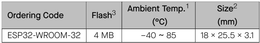
1.2 Ordering Information
ESP32-WROOM-32 is a powerful, generic Wi-Fi + Bluetooth® + Bluetooth LE MCU module that targets a wide variety of applications, ranging from low-power sensor networks to the most demanding tasks, such as voice encoding, music streaming and MP3 decoding.
ESP32-WROOM-32 comes with a PCB antenna. The module features a 4 MB external SPI flash.
The ordering information for the modules is as follows:
Table 1: ESP32-WROOM-32 Ordering Information
| Ordering Code | Flash3 | Ambient Temp.1(°C) | Size2(mm) |
| ESP32-WROOM-32 | 4 MB | -40 ~ 85 | 18 × 25.5 × 3.1 |
1 Ambient temperature specifies the recommended temperature range of the environment immediately outside the Espressif module.
2 For details, refer to Section 9 Module Dimensions.
3 For specifications, refer to Section 5.5 Memory Specifications.
At the core of this module is the ESP32-D0WDQ6, an Xtensa® 32-bit LX7 CPU that operates at up to 240 MHz. You can power off the CPU and make use of the low-power coprocessor to constantly monitor the peripherals for changes or crossing of thresholds.
Note:
• For details on the part numbers of the ESP32 family of chips, please refer to the document ESP32 Datasheet.
For chip revision identification, ESP-IDF release that supports a specific chip revision, and other information on chip revisions, please refer to ESP32 Series SoC Errata > Section Chip Revision Identification.
1.3 Applications
Smart Home
Industrial Automation
Health Care
Consumer Electronics
Smart Agriculture
POS Machines
Service Robot
Audio Devices
Generic Low-power IoT Sensor Hubs
• Generic Low-power IoT Data Loggers
• Cameras for Video Streaming
• Speech Recognition
• Image Recognition
SDIO Wi-Fi + Bluetooth Networking Card
Contents
1 Module Overview 2
1.1 Features 2
1.2 Ordering Information 2
1.3 Applications 3
2 Pin Definitions 8
2.1 Pin Layout 8
2.2 Pin Description 8
3 Boot Configurations 11
3.1 Chip Boot Mode Control 12
3.2 Internal LDO (VDD_SDIO) Voltage Control 13
3.3 U0TXD Printing Control 14
3.4 Timing Control of SDIO Slave 14
3.5 JTAG Signal Source Control 14
3.6 Chip Power-up and Reset 14
4 Peripherals 16
4.1 Peripheral Overview 16
4.2 Digital Peripherals 16
4.2.1 General Purpose Input / Output Interface (GPIO) 16
4.2.2 Serial Peripheral Interface (SPI) 16
4.2.3 Universal Asynchronous Receiver Transmitter (UART) 17
4.2.4 I2C Interface 17
4.2.5 I2S Interface 18
4.2.6 Remote Control Peripheral 18
4.2.7 Pulse Counter Controller (PCNT) 19
4.2.8 LED PWM Controller 19
4.2.9 Motor Control PWM 20
4.2.10 SD/SDIO/MMC Host Controller 21
4.2.11 SDIO/SPI Slave Controller 21
4.2.12 TWAI® Controller 22
4.2.13 Ethernet MAC Interface 23
4.3 Analog Peripherals 23
4.3.1 Analog-to-Digital Converter (ADC) 23
4.3.2 Digital-to-Analog Converter (DAC) 24
4.3.3 Touch Sensor 25
5 Electrical Characteristics 26
5.1 Absolute Maximum Ratings 26
5.2 Recommended Operating Conditions 26
5.3 DC Characteristics (3.3 V, 25 °C) 26
5.4 Current Consumption Characteristics 27
Not Recommended For New Designs (NRND)
5.5 Memory Specifications 27
6 RF Characteristics 28
6.1 Wi-Fi Radio 28
6.1.1 Wi-Fi RF Transmitter (TX) Characteristics 28
6.1.2 Wi-Fi RF Receiver (RX) Characteristics 29
6.2 Bluetooth LE Radio 30
6.2.1 Receiver 30
6.2.2 Transmitter 31
7 Module Schematics 33
8 Peripheral Schematics 34
9 Module Dimensions 35
10 PCB Layout Recommendations 36
10.1 PCB Land Pattern 36
10.2 Module Placement for PCB Design 37
11 Product Handling 38
11.1 Storage Conditions 38
11.2 Electrostatic Discharge (ESD) 38
11.3 Reflow Profile 38
11.4 Ultrasonic Vibration 39
Datasheet Versioning 40
Related Documentation and Resources 41
Revision History 42
List of Tables
1 ESP32-WROOM-32 Ordering Information 3
2 Pin Definitions 9
3 Default Configuration of Strapping Pins 11
4 Description of Timing Parameters for the Strapping Pins 12
5 Chip Boot Mode Control 12
6 U0TXD Printing Control 14
7 Timing Control of SDIO Slave 14
8 Description of Timing Parameters for Power-up and Reset 15
9 ADC Characteristics 24
10 ADC Calibration Results 24
11 Capacitive-Sensing GPIOs Available on ESP32 25
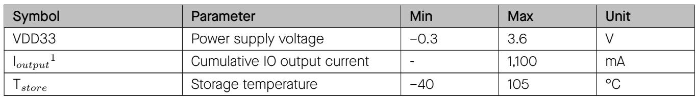
12 Absolute Maximum Ratings 26
13 Recommended Operating Conditions 26
14 DC Characteristics (3.3 V, 25 °C) 26
15 Flash Specifications 27
16 Wi-Fi RF Characteristics 28
17 TX Power with Spectral Mask and EVM Meeting 802.11 Standards 28
18 TX EVM Test1 28
19 RX Sensitivity 29
20 Maximum RX Level 30
21 RX Adjacent Channel Rejection 30
22 Receiver Characteristics – Bluetooth LE 30
23 Transmitter Characteristics – Bluetooth LE 31
List of Figures
1 ESP32-WROOM-32 Pin Layout (Top View) 8
2 Visualization of Timing Parameters for the Strapping Pins 12
3 Chip Boot Flow 13
4 Visualization of Timing Parameters for Power-up and Reset 14
5 ESP32-WROOM-32 Schematics 33
6 ESP32-WROOM-32 Peripheral Schematics 34
Physical Dimensions 35
8 Recommended PCB Land Pattern 36
9 Reflow Profile 38
2 Pin Definitions
2.1 Pin Layout
The pin diagram below shows the approximate location of pins on the module. For the actual diagram drawn to scale, please refer to Figure 9 Module Dimensions.
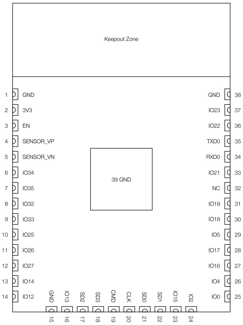
text_image
Keepout Zone
1 GND GND 38
2 3V3 IO23 37
3 EN IO22 36
4 SENSOR_VP TXD0 35
5 SENSOR_VN RXD0 34
6 IO34 IO21 33
7 IO35 NC 32
8 IO32 IO19 31
9 IO33 IO18 30
10 IO25 IO5 29
11 IO26 IO17 28
12 IO27 IO16 27
13 IO14 IO4 26
14 IO12 IO0 25
GND IO13 SD2 SD3 CMD CLK SD0 SD1 IO15 IO2
15 16 17 18 19 20 21 22 23 24
Figure 1: ESP32-WROOM-32 Pin Layout (Top View)
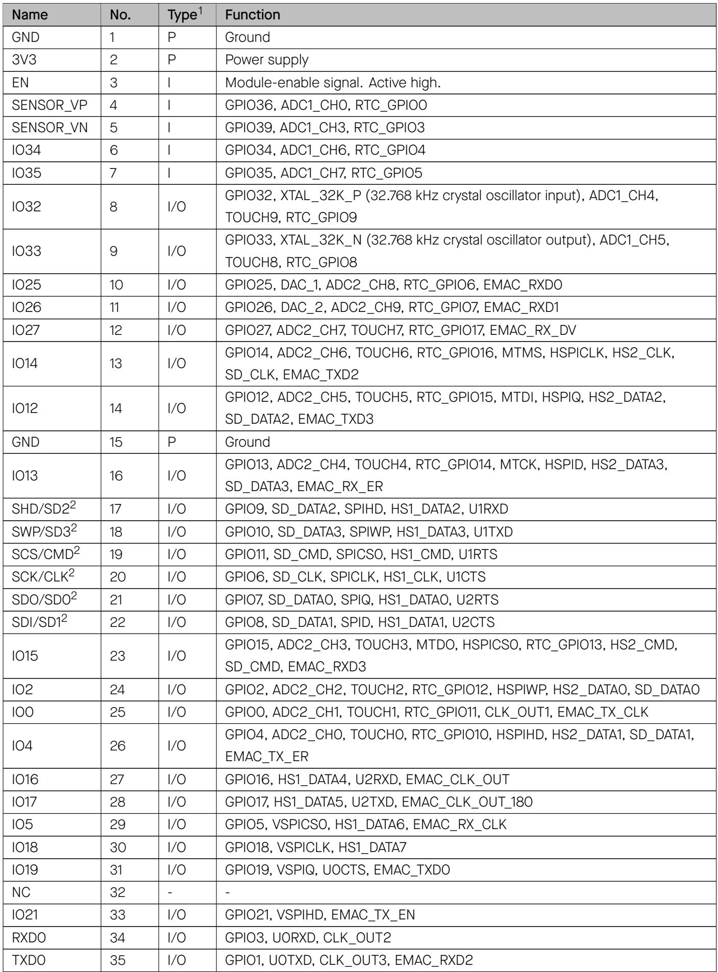
2.2 Pin Description
ESP32-WROOM-32 has 38 pins. See pin definitions in Table 2.
For peripheral pin configurations, please refer to Section 4.2 Digital Peripherals.
Table 2: Pin Definitions
1 P: power supply; I: input; O: output.
| Name | No. | $Type^1$ | Function |
| GND | 1 | P | Ground |
| 3V3 | 2 | P | Power supply |
| EN | 3 | I | Module-enable signal. Active high. |
| SENSOR_VP | 4 | I | GPIO36, ADC1_CHO, RTC_GPIO0 |
| SENSOR_VN | 5 | I | GPIO39, ADC1_CH3, RTC_GPIO3 |
| IO34 | 6 | I | GPIO34, ADC1_CH6, RTC_GPIO4 |
| IO35 | 7 | I | GPIO35, ADC1_CH7, RTC_GPIO5 |
| IO32 | 8 | I/O | GPIO32, XTAL_32K_P (32.768 kHz crystal oscillator input), ADC1_CH4, TOUCH9, RTC_GPIO9 |
| IO33 | 9 | I/O | GPIO33, XTAL_32K_N (32.768 kHz crystal oscillator output), ADC1_CH5, TOUCH8, RTC_GPIO8 |
| IO25 | 10 | I/O | GPIO25, DAC_1, ADC2_CH8, RTC_GPIO6, EMAC_RXDO |
| IO26 | 11 | I/O | GPIO26, DAC_2, ADC2_CH9, RTC_GPIO7, EMAC_RXD1 |
| IO27 | 12 | I/O | GPIO27, ADC2_CH7, TOUCH7, RTC_GPIO17, EMAC_RX_DV |
| IO14 | 13 | I/O | GPIO14, ADC2_CH6, TOUCH6, RTC_GPIO16, MTMS, HSPICLK, HS2_CLK, SD_CLK, EMAC_TXD2 |
| IO12 | 14 | I/O | GPIO12, ADC2_CH5, TOUCH5, RTC_GPIO15, MTDI, HSPIQ, HS2_DATA2, SD_DATA2, EMAC_TXD3 |
| GND | 15 | P | Ground |
| IO13 | 16 | I/O | GPIO13, ADC2_CH4, TOUCH4, RTC_GPIO14, MTCK, HSPID, HS2_DATA3, SD_DATA3, EMAC_RX_ER |
| $SHD/SD2^2$ | 17 | I/O | GPIO9, SD_DATA2, SPIHD, HS1_DATA2, U1RXD |
| $SWP/SD3^2$ | 18 | I/O | GPIO10, SD_DATA3, SPIWP, HS1_DATA3, U1TXD |
| $SCS/CMD^2$ | 19 | I/O | GPIO11, SD_CMD, SPICS0, HS1_CMD, U1RTS |
| $SCK/CLK^2$ | 20 | I/O | GPIO6, SD_CLK, SPICLK, HS1_CLK, U1CTS |
| $SDO/SDO^2$ | 21 | I/O | GPIO7, SD_DATA0, SPIQ, HS1_DATA0, U2RTS |
| $SDI/SD1^2$ | 22 | I/O | GPIO8, SD_DATA1, SPID, HS1_DATA1, U2CTS |
| IO15 | 23 | I/O | GPIO15, ADC2_CH3, TOUCH3, MTDO, HSPICS0, RTC_GPIO13, HS2_CMD, SD_CMD, EMAC_RXD3 |
| IO2 | 24 | I/O | GPIO2, ADC2_CH2, TOUCH2, RTC_GPIO12, HSPIWP, HS2_DATA0, SD_DATA0 |
| IO0 | 25 | I/O | GPIO0, ADC2_CH1, TOUCH1, RTC_GPIO11, CLK_OUT1, EMAC_TX_CLK |
| IO4 | 26 | I/O | GPIO4, ADC2_CHO, TOUCH0, RTC_GPIO10, HSPIHD, HS2_DATA1, SD_DATA1, EMAC_TX_ER |
| IO16 | 27 | I/O | GPIO16, HS1_DATA4, U2RXD, EMAC_CLK_OUT |
| IO17 | 28 | I/O | GPIO17, HS1_DATA5, U2TXD, EMAC_CLK_OUT_180 |
| IO5 | 29 | I/O | GPIO5, VSPICS0, HS1_DATA6, EMAC_RX_CLK |
| IO18 | 30 | I/O | GPIO18, VSPICLK, HS1_DATA7 |
| IO19 | 31 | I/O | GPIO19, VSPIQ, UOCTS, EMAC_TXDO |
| NC | 32 | - | - |
| IO21 | 33 | I/O | GPIO21, VSPIHD, EMAC_TX_EN |
| RXDO | 34 | I/O | GPIO3, UORXD, CLK_OUT2 |
| TXDO | 35 | I/O | GPIO1, UOTXD, CLK_OUT3, EMAC_RXD2 |
| Name | No. | Type1 | Function |
| IO22 | 36 | I/O | GPIO22, VSPIWP, UORTS, EMAC_TXD1 |
| IO23 | 37 | I/O | GPIO23, VSPID, HS1_STROBE |
| GND | 38 | P | Ground |
2 Pins SCK/CLK, SDO/SD0, SDI/SD1, SHD/SD2, SWP/SD3 and SCS/CMD, namely, GPIO6 to GPIO11 on the ESP32- D0WDQ6 chip are connected to the SPI flash integrated on the module and are not recommended for other uses.
3 Boot Configurations
Note:
The content below is excerpted from ESP32 Series Datasheet > Section Boot Configurations. For the strapping pin mapping between the chip and modules, please refer to Chapter 7 Module Schematics.
The chip allows for configuring the following boot parameters through strapping pins and eFuse bits at power-up or a hardware reset, without microcontroller interaction.
• Chip boot mode
– Strapping pin: GPIO0 and GPIO2
• Internal LDO (VDD_SDIO) Voltage
– Strapping pin: MTDI
– eFuse bit: EFUSE_SDIO_FORCE and EFUSE_SDIO_TIEH
• U0TXD printing
– Strapping pin: MTDO
• Timing of SDIO Slave
– Strapping pin: MTDO and GPIO5
• JTAG signal source
– eFuse bit: EFUSE_DISABLE_JTAG
The default values of all the above eFuse bits are 0, which means that they are not burnt. Given that eFuse is one-time programmable, once an eFuse bit is programmed to 1, it can never be reverted to 0. For how to program eFuse bits, please refer to ESP32 Technical Reference Manual > Chapter eFuse Controller.
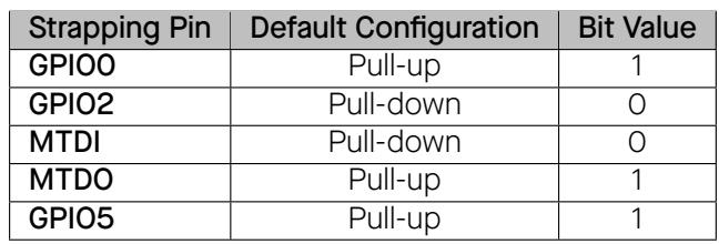
The default values of the strapping pins, namely the logic levels, are determined by pins’ internal weak pull-up/pull-down resistors at reset if the pins are not connected to any circuit, or connected to an external high-impedance circuit.
Table 3: Default Configuration of Strapping Pins
| Strapping Pin | Default Configuration | Bit Value |
| GPIO0 | Pull-up | 1 |
| GPIO2 | Pull-down | 0 |
| MTDI | Pull-down | 0 |
| MTDO | Pull-up | 1 |
| GPIO5 | Pull-up | 1 |
To change the bit values, the strapping pins should be connected to external pull-down/pull-up resistances. If the ESP32 is used as a device by a host MCU, the strapping pin voltage levels can also be controlled by the host MCU.
All strapping pins have latches. At system reset, the latches sample the bit values of their respective strapping pins and store them until the chip is powered down or shut down. The states of latches cannot be changed in any other way. It makes the strapping pin values available during the entire chip operation, and the pins are freed up to be used as regular IO pins after reset.
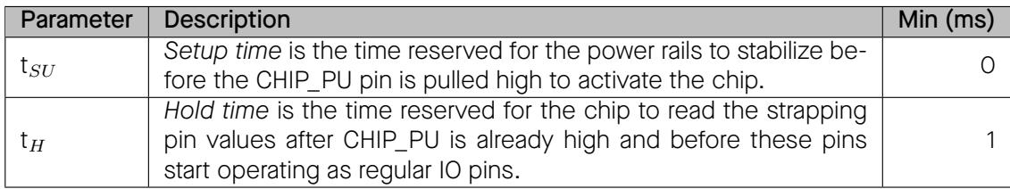
The timing of signals connected to the strapping pins should adhere to the setup time and hold time specifications in Table 4 and Figure 2.
Table 4: Description of Timing Parameters for the Strapping Pins
| Parameter | Description | Min (ms) |
| $t_{SU}$ | Setup time is the time reserved for the power rails to stabilize before the CHIP_PU pin is pulled high to activate the chip. | 0 |
| $t_H$ | Hold time is the time reserved for the chip to read the strapping pin values after CHIP_PU is already high and before these pins start operating as regular IO pins. | 1 |
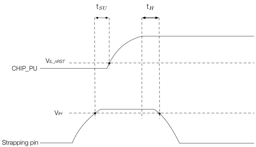
line
| Timepoint | Voltage Level |
|---|---|
| tSU | V_IL_nRST |
| tSU | V_IH |
| tH | V_IH |
Figure 2: Visualization of Timing Parameters for the Strapping Pins
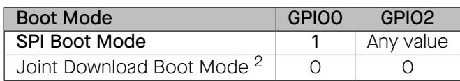
3.1 Chip Boot Mode Control
GPIO0 and GPIO2 control the boot mode after the reset is released. See Table 5 Chip Boot Mode Control.
Table 5: Chip Boot Mode Control
| Boot Mode | GPIO0 | GPIO2 |
| SPI Boot Mode | 1 | Any value |
| Joint Download Boot $Mode^2$ | 0 | 0 |
1 Bold marks the default value and configuration.
2 Joint Download Boot mode supports the following download methods:
SDIO Download Boot
UART Download Boot
In Joint Download Boot mode, the detailed boot flow of the chip is put below 3.
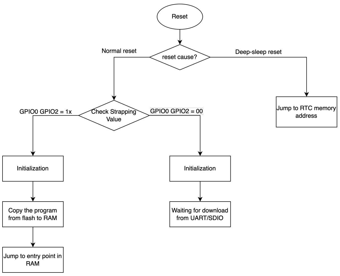
flowchart
graph TD
    A["Reset"] --> B{reset cause?}
    B -->|Normal reset| C{Check Strapping Value}
    B -->|Deep-sleep reset| D["Jump to RTC memory address"]
    C -->|GPIO0 GPIO2 = 1x| E["Initialization"]
    C -->|GPIO0 GPIO2 = 00| F["Initialization"]
    E --> G["Copy the program from flash to RAM"]
    F --> H["Waiting for download from UART/SDIO"]
    G --> I["Jump to entry point in RAM"]
Figure 3: Chip Boot Flow
uart_download_dis controls boot mode behaviors:
It permanently disables Download Boot mode when uart_download_dis is set to 1 (valid only for ESP32 chip revisions v3.0 and higher).
3.2 Internal LDO (VDD_SDIO) Voltage Control
MTDI is used to select the VDD_SDIO power supply voltage at reset:
MTDI = 0 (by default), VDD_SDIO pin is powered directly from VDD3P3_RTC. Typically this voltage is 3.3 V. For more information, see ESP32 Series Datasheet > Section Power Scheme.
MTDI = 1, VDD_SDIO pin is powered from internal 1.8 V LDO.
This functionality can be overridden by setting EFUSE_SDIO_FORCE to 1, in which case the EFUSE_SDIO_TIEH determines the VDD_SDIO voltage:
EFUSE_SDIO_TIEH = 0, VDD_SDIO connects to 1.8 V LDO.
EFUSE_SPI_TIEH = 1, VDD_SDIO connects to VDD3P3_RTC.
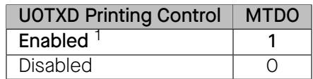
3.3 U0TXD Printing Control
During booting, the strapping pin MTDO can be used to control the U0TXD Printing, as Table 6 shows.
Table 6: U0TXD Printing Control
| UOTXD Printing Control | MTDO |
| Enabled1 | 1 |
| Disabled | 0 |
1 Bold marks the default value and configuration.
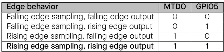
3.4 Timing Control of SDIO Slave
The strapping pin MTDO and GPIO5 can be used to control the timing of SDIO slave, see Table 7 Timing Control of SDIO Slave.
Table 7: Timing Control of SDIO Slave
| Edge behavior | MTDO | GPIO5 |
| Falling edge sampling, falling edge output | 0 | 0 |
| Falling edge sampling, rising edge output | 0 | 1 |
| Rising edge sampling, falling edge output | 1 | 0 |
| Rising edge sampling, rising edge output | 1 | 1 |
1 Bold marks the default value and configuration.
3.5 JTAG Signal Source Control
If EFUSE_DISABLE_JTAG is set to 1, the source of JTAG signals can be disabled.
3.6 Chip Power-up and Reset
Once the power is supplied to the chip, its power rails need a short time to stabilize. After that, CHIP_PU – the pin used for power-up and reset – is pulled high to activate the chip. For information on CHIP_PU as well as power-up and reset timing, see Figure 4 and Table 8.
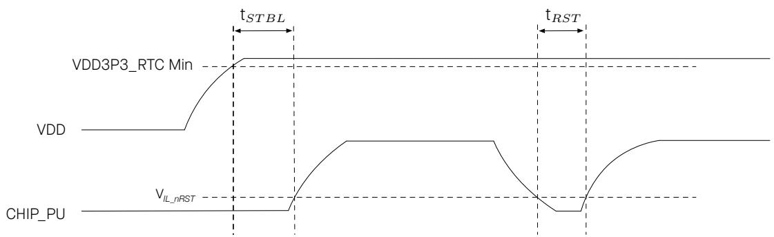
line
| Signal | Time Segment |
|---|---|
| VDD3P3_RTC_Min | t_STBL |
| VDD | t_RST |
| CHIP_PU | V_IL_nRST |
Figure 4: Visualization of Timing Parameters for Power-up and Reset
Table 8: Description of Timing Parameters for Power-up and Reset
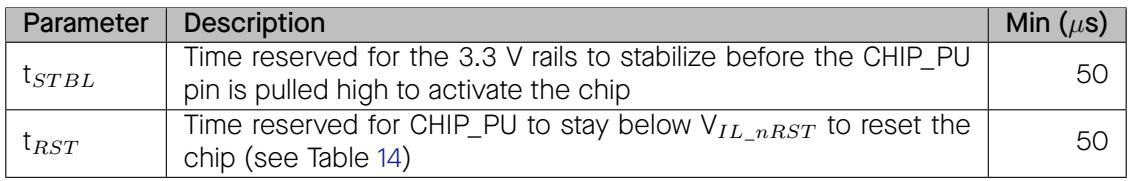
| Parameter | Description | Min ( $\mu s$ ) |
| $t_{STBL}$ | Time reserved for the 3.3 V rails to stabilize before the CHIP_PU pin is pulled high to activate the chip | 50 |
| $t_{RST}$ | Time reserved for CHIP_PU to stay below $V_{IL\_nRST}$ to reset the chip (see Table 14) | 50 |
For details, please refer to ESP32 Series Datasheet > Section Chip Power-up and Reset.
4 Peripherals
4.1 Peripheral Overview
ESP32-D0WDQ6 chip integrates a rich set of peripherals including SPI, I2S, UART, I2C, pulse count controller, TWAI®, ADC, DAC, touch sensor, etc.
To learn more about on-chip components, please refer to ESP32 Series Datasheet > Section Functional Description.
Note:
The content below is sourced from ESP32 Series Datasheet > Section Functional Description. Some information may not be applicable to ESP32-WROOM-32 as not all the IO signals are exposed on the module.
• To learn more about peripheral signals, please refer to ESP32 Technical Reference Manual > Section Peripheral Signal List.
4.2 Digital Peripherals
4.2.1 General Purpose Input / Output Interface (GPIO)
ESP32 has 34 GPIO pins which can be assigned various functions by programming the appropriate registers. There are several kinds of GPIOs: digital-only, analog-enabled, capacitive-touch-enabled, etc. Analog-enabled GPIOs and Capacitive-touch-enabled GPIOs can be configured as digital GPIOs.
Most of the digital GPIOs can be configured as internal pull-up or pull-down, or set to high impedance. When configured as an input, the input value can be read through the register. The input can also be set to edge-trigger or level-trigger to generate CPU interrupts. Most of the digital IO pins are bi-directional, non-inverting and tristate, including input and output buffers with tristate control. These pins can be multiplexed with other functions, such as the SDIO, UART, SPI, etc. (More details can be found in ESP32 Series Datasheet > Appendix, Table IO_MUX. ) For low-power operations, the GPIOs can be set to hold their states.
For details, see ESP32 Series Datasheet > Section Peripheral Pin Configurations, ESP32 Series Datasheet > Appendix A – ESP32 Pin Lists and ESP32 Technical Reference Manual > Chapter IO_MUX and GPIO Matrix.
4.2.2 Serial Peripheral Interface (SPI)
ESP32 integrates four SPI controllers which can be used to communicate with external devices that use the SPI protocol. Controller SPI0 is used as a buffer for accessing external memory. Controller SPI1 can be used as a master. Controllers SPI2 and SPI3 can be configured as either a master or a slave.
SPI1, SPI2, and SPI3 use signal buses prefixed with SPI, HSPI, and VSPI, respectively.
Features of General Purpose SPI (GP-SPI)
Programmable data transfer length, in multiples of 1 byte
Four-line full-duplex/half-duplex communication and three-line half-duplex communication support
Master mode and slave mode
• Programmable CPOL and CPHA
• Programmable clock
For details, see ESP32 Technical Reference Manual > Chapter SPI Controller.
Pin Assignment
For SPI, the pins are multiplexed with GPIO6 ~ GPIO11 via the IO MUX. For HSPI, the pins are multiplexed with GPIO2, GPIO4, GPIO12 ~ GPIO15 via the IO MUX. For VSPI, the pins are multiplexed with GPIO5, GPIO18 ~ GPIO19, GPIO21 ~ GPIO23 via the IO MUX.
For more information about the pin assignment, see ESP32 Series Datasheet > Section Peripheral Pin Configurations and ESP32 Technical Reference Manual > Chapter IO_MUX and GPIO Matrix.
4.2.3 Universal Asynchronous Receiver Transmitter (UART)
The UART in the ESP32 chip facilitates the transmission and reception of asynchronous serial data between the chip and external UART devices. It consists of two UARTs in the main system, and one low-power LP UART.
Feature List
Programmable baud rate
RAM shared by TX FIFOs and RX FIFOs
• Supports input baud rate self-check
Support for various lengths of data bits and stop bits
Parity bit support
• Asynchronous communication (RS232 and RS485) and IrDA support
• Supports DMA to communicate data in high speed
• Supports UART wake-up
Supports both software and hardware flow control
For details, see ESP32 Technical Reference Manual > Chapter UART Controller.
Pin Assignment
The pins for UART can be chosen from any GPIOs via the GPIO Matrix.
For more information about the pin assignment, see ESP32 Series Datasheet > Section Peripheral Pin Configurations and ESP32 Technical Reference Manual > Chapter IO_MUX and GPIO Matrix.
4.2.4 I2C Interface
ESP32 has two I2C bus interfaces which can serve as I2C master or slave, depending on the user’s configuration.
Feature List
• Two I2C controllers: one in the main system and one in the low-power system
Standard mode (100 Kbit/s)
• Fast mode (400 Kbit/s)
• Up to 5 MHz, yet constrained by SDA pull-up strength
Support for 7-bit and 10-bit addressing, as well as dual address mode
• Supports continuous data transmission with disabled Serial Clock Line (SCL)
• Supports programmable digital noise filter
Users can program command registers to control I2C interfaces, so that they have more flexibility.
For details, see ESP32 Technical Reference Manual > Chapter I2C Controller.
Pin Assignment
For regular I2C, the pins used can be chosen from any GPIOs via the GPIO Matrix.
For more information about the pin assignment, see ESP32 Series Datasheet > Section Peripheral Pin Configurations and ESP32 Technical Reference Manual > Chapter IO_MUX and GPIO Matrix.
4.2.5 I2S Interface
The I2S Controller in the ESP32 chip provides a flexible communication interface for streaming digital data in multimedia applications, particularly digital audio applications.
Feature List
Master mode and slave mode
• Full-duplex and half-duplex communications
A variety of audio standards supported
Configurable high-precision output clock
Supports PDM signal input and output
Configurable data transmit and receive modes
For details, see ESP32 Technical Reference Manual > Chapter I2S Controller.
Pin Assignment
The pins for the I2S Controller can be chosen from any GPIOs via the GPIO Matrix.
For more information about the pin assignment, see ESP32 Series Datasheet > Section Peripheral Pin Configurations and ESP32 Technical Reference Manual > Chapter IO_MUX and GPIO Matrix.
4.2.6 Remote Control Peripheral
The Remote Control Peripheral (RMT) controls the transmission and reception of infrared remote control signals.
Feature List
• Eight channels for sending and receiving infrared remote control signals
Independent transmission and reception capabilities for each channel
Clock divider counter, state machine, and receiver for each RX channel
Supports various infrared protocols
For details, see ESP32 Technical Reference Manual > Chapter Remote Control Peripheral.
Pin Assignment
The pins for the Remote Control Peripheral can be chosen from any GPIOs via the GPIO Matrix.
For more information about the pin assignment, see ESP32 Series Datasheet > Section Peripheral Pin Configurations and ESP32 Technical Reference Manual > Chapter IO_MUX and GPIO Matrix.
4.2.7 Pulse Counter Controller (PCNT)
The pulse counter controller (PCNT) is designed to count input pulses by tracking rising and falling edges of the input pulse signal.
Feature List
• Eight independent pulse counter units
Each pulse counter unit has a 16-bit signed counter register and two channels
Counter modes: increment, decrement, or disable
• Glitch filtering for input pulse signals and control signals
• Selection between counting on rising or falling edges of the input pulse signal
For details, see ESP32 Technical Reference Manual > Chapter Pulse Count Controller.
Pin Assignment
The pins for the Pulse Count Controller can be chosen from any GPIOs via the GPIO Matrix.
For more information about the pin assignment, see ESP32 Series Datasheet > Section Peripheral Pin Configurations and ESP32 Technical Reference Manual > Chapter IO_MUX and GPIO Matrix.
4.2.8 LED PWM Controller
The LED PWM Controller (LEDC) is designed to generate PWM signals for LED control.
Feature List
• Sixteen independent PWM generators
Maximum PWM duty cycle resolution of 20 bits
• Eight independent timers with 20-bit counters, configurable fractional clock dividers and counter overflow values
• Adjustable phase of PWM signal output
• PWM duty cycle dithering
• Automatic duty cycle fading
For details, see ESP32 Technical Reference Manual > Chapter LED PWM Controller.
Pin Assignment
The pins for the LED PWM Controller can be chosen from any GPIOs via the GPIO Matrix.
For more information about the pin assignment, see ESP32 Series Datasheet > Section Peripheral Pin Configurations and ESP32 Technical Reference Manual > Chapter IO_MUX and GPIO Matrix.
4.2.9 Motor Control PWM
The Pulse Width Modulation (PWM) controller can be used for driving digital motors and smart lights. The controller consists of PWM timers, the PWM operator and a dedicated capture sub-module. Each timer provides timing in synchronous or independent form, and each PWM operator generates a waveform for one PWM channel. The dedicated capture sub-module can accurately capture events with external timing.
Feature List
• Three PWM timers for precise timing and frequency control
– Every PWM timer has a dedicated 8-bit clock prescaler
– The 16-bit counter in the PWM timer can work in count-up mode, count-down mode, or count-up-down mode
– A hardware sync can trigger a reload on the PWM timer with a phase register. It will also trigger the prescaler’ restart, so that the timer’s clock can also be synced, with selectable hardware synchronization source
• Three PWM operators for generating waveform pairs
– Six PWM outputs to operate in several topologies
– Configurable dead time on rising and falling edges; each set up independently
– Modulating of PWM output by high-frequency carrier signals, useful when gate drivers are insulated with a transformer
Fault Detection module
– Programmable fault handling in both cycle-by-cycle mode and one-shot mode
– A fault condition can force the PWM output to either high or low logic levels
• Capture module for hardware-based signal processing
– Speed measurement of rotating machinery
– Measurement of elapsed time between position sensor pulses
– Period and duty cycle measurement of pulse train signals
– Decoding current or voltage amplitude derived from duty-cycle-encoded signals of current/voltage sensors
– Three individual capture channels, each of which with a 32-bit time-stamp register
– Selection of edge polarity and prescaling of input capture signals
– The capture timer can sync with a PWM timer or external signals
For details, see ESP32 Technical Reference Manual > Chapter Motor Control PWM.
Pin Assignment
The pins for the Motor Control PWM can be chosen from any GPIOs via the GPIO Matrix.
For more information about the pin assignment, see ESP32 Series Datasheet > Section Peripheral Pin Configurations and ESP32 Technical Reference Manual > Chapter IO_MUX and GPIO Matrix.
4.2.10 SD/SDIO/MMC Host Controller
An SD/SDIO/MMC host controller is available on ESP32.
Feature List
Supports two external cards
Supports SD Memory Card standard: version 3.0 and version 3.01)
Supports SDIO Version 3.0
• Supports Consumer Electronics Advanced Transport Architecture (CE-ATA Version 1.1)
• Supports Multimedia Cards (MMC version 4.41, eMMC version 4.5 and version 4.51)
The controller allows up to 80 MHz clock output in three different data-bus modes: 1-bit, 4-bit, and 8-bit modes. It supports two SD/SDIO/MMC4.41 cards in a 4-bit data-bus mode. It also supports one SD card operating at 1.8 V.
For details, see ESP32 Technical Reference Manual > Chapter SD/MMC Host Controller.
Pin Assignment
The pins for SD/SDIO/MMC Host Controller are multiplexed with GPIO2, GPIO4, GPIO6 ~ GPIO15 via IO MUX.
For more information about the pin assignment, see ESP32 Series Datasheet > Section Peripheral Pin Configurations and ESP32 Technical Reference Manual > Chapter IO_MUX and GPIO Matrix.
4.2.11 SDIO/SPI Slave Controller
ESP32 integrates an SD device interface that conforms to the industry-standard SDIO Card Specification Version 2.0, and allows a host controller to access the SoC, using the SDIO bus interface and protocol. ESP32 acts as the slave on the SDIO bus. The host can access the SDIO-interface registers directly and can access shared memory via a DMA engine, thus maximizing performance without engaging the processor cores.
Feature List
The SDIO/SPI slave controller supports the following features:
• SPI, 1-bit SDIO, and 4-bit SDIO transfer modes over the full clock range from 0 to 50 MHz
• Configurable sampling and driving clock edge
Special registers for direct access by host
Interrupts to host for initiating data transfer
• Automatic loading of SDIO bus data and automatic discarding of padding data
• Block size of up to 512 bytes
• Interrupt vectors between the host and the slave, allowing both to interrupt each other
Supports DMA for data transfer
For details, see ESP32 Technical Reference Manual > Chapter SDIO Slave Controller.
Pin Assignment
The pins for SDIO/SPI Slave Controller are multiplexed with GPIO2, GPIO4, GPIO6 ~ GPIO15 via IO MUX.
For more information about the pin assignment, see ESP32 Series Datasheet > Section Peripheral Pin Configurations and ESP32 Technical Reference Manual > Chapter IO_MUX and GPIO Matrix.
4.2.12 TWAI® Controller
The Two-wire Automotive Interface (TWAI®) is a multi-master, multi-cast communication protocol designed for automotive applications. The TWAI controller facilitates the communication based on this protocol.
Feature List
• Compatible with ISO 11898-1 protocol (CAN Specification 2.0)
Standard frame format (11-bit ID) and extended frame format (29-bit ID)
Bit rates:
– From 25 Kbit/s to 1 Mbit/s in chip revision v0.0/v1.0/v1.1
– From 12.5 Kbit/s to 1 Mbit/s in chip revision v3.0/v3.1
Multiple modes of operation: Normal, Listen Only, and Self-Test
64-byte receive FIFO
Special transmissions: single-shot transmissions and self reception
Acceptance filter (single and dual filter modes)
• Error detection and handling: error counters, configurable error interrupt threshold, error code capture, arbitration lost capture
For details, see ESP32 Technical Reference Manual > Chapter Two-wire Automotive Interface (TWAI).
Pin Assignment
The pins for the Two-wire Automotive Interface can be chosen from any GPIOs via the GPIO Matrix.
For more information about the pin assignment, see ESP32 Series Datasheet > Section Peripheral Pin Configurations and ESP32 Technical Reference Manual > Chapter IO_MUX and GPIO Matrix.
4.2.13 Ethernet MAC Interface
An IEEE-802.3-2008-compliant Media Access Controller (MAC) is provided for Ethernet LAN communications. ESP32 requires an external physical interface device (PHY) to connect to the physical LAN bus (twisted-pair, fiber, etc.). The PHY is connected to ESP32 through 17 signals of MII or nine signals of RMII.
Feature List
• 10 Mbps and 100 Mbps rates
• Dedicated DMA controller allowing high-speed transfer between the dedicated SRAM and Ethernet MAC
• Tagged MAC frame (VLAN support)
Half-duplex (CSMA/CD) and full-duplex operation
MAC control sublayer (control frames)
32-bit CRC generation and removal
Several address-filtering modes for physical and multicast address (multicast and group addresses)
32-bit status code for each transmitted or received frame
Internal FIFOs to buffer transmit and receive frames. The transmit FIFO and the receive FIFO are both 512 words (32-bit)
Hardware PTP (Precision Time Protocol) in accordance with IEEE 1588 2008 (PTP V2)
25 MHz/50 MHz clock output
For details, see ESP32 Technical Reference Manual > Chapter Ethernet Media Access Controller (MAC).
Pin Assignment
For information about the pin assignment of Ethernet MAC Interface, see ESP32 Series Datasheet > Section Peripheral Pin Configurations and ESP32 Technical Reference Manual > Chapter IO_MUX and GPIO Matrix.
4.3 Analog Peripherals
4.3.1 Analog-to-Digital Converter (ADC)
ESP32 integrates two 12-bit SAR ADCs and supports measurements on 18 channels (analog-enabled pins). The ULP coprocessor in ESP32 is also designed to measure voltage, while operating in the sleep mode, which enables low-power consumption. The CPU can be woken up by a threshold setting and/or via other triggers.
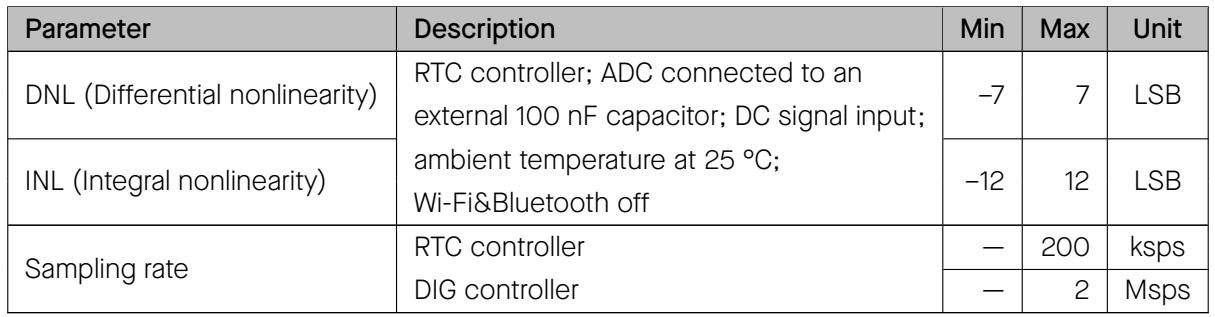
Table 9 describes the ADC characteristics.
Table 9: ADC Characteristics
| Parameter | Description | Min | Max | Unit |
| DNL (Differential nonlinearity) | RTC controller; ADC connected to an external 100 nF capacitor; DC signal input; ambient temperature at 25 °C; Wi-Fi&Bluetooth off | -7 | 7 | LSB |
| INL (Integral nonlinearity) | -12 | 12 | LSB | |
| Sampling rate | RTC controller | — | 200 | ksps |
| DIG controller | — | 2 | Msps |
Notes:
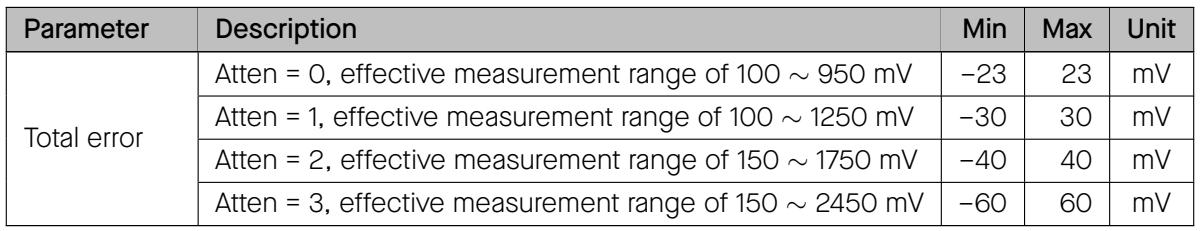
• When atten = 3 and the measurement result is above 3000 (voltage at approx. 2450 mV), the ADC accuracy will be worse than described in the table above.
• To get better DNL results, users can take multiple sampling tests with a filter, or calculate the average value.
The input voltage range of GPIO pins within VDD3P3_RTC domain should strictly follow the DC characteristics provided in Table 14. Otherwise, measurement errors may be introduced, and chip performance may be affected.
By default, there are ±6% differences in measured results between chips. ESP-IDF provides couple of calibration methods for ADC1. Results after calibration using eFuse Vref value are shown in Table 10. For higher accuracy, users may apply other calibration methods provided in ESP-IDF, or implement their own.
Table 10: ADC Calibration Results
| Parameter | Description | Min | Max | Unit |
| Total error | Atten = 0, effective measurement range of 100 ~ 950 mV | -23 | 23 | mV |
| Atten = 1, effective measurement range of 100 ~ 1250 mV | -30 | 30 | mV | |
| Atten = 2, effective measurement range of 150 ~ 1750 mV | -40 | 40 | mV | |
| Atten = 3, effective measurement range of 150 ~ 2450 mV | -60 | 60 | mV |
For details, see ESP32 Technical Reference Manual > Chapter On-Chip Sensors and Analog Signal Processing.
Pin Assignment
With appropriate settings, the ADCs can be configured to measure voltage on 18 pins maximum. For detailed information about the pin assignment, see ESP32 Series Datasheet > Section Peripheral Pin Configurations and ESP32 Technical Reference Manual > Chapter IO_MUX and GPIO Matrix.
4.3.2 Digital-to-Analog Converter (DAC)
Two 8-bit DAC channels can be used to convert two digital signals into two analog voltage signal outputs. The design structure is composed of integrated resistor strings and a buffer. This dual DAC supports power supply as input voltage reference. The two DAC channels can also support independent conversions.
For details, see ESP32 Technical Reference Manual > Chapter On-Chip Sensors and Analog Signal Processing.
Pin Assignment
The DAC can be configured by GPIO 25 and GPIO 26. For detailed information about the pin assignment, see ESP32 Series Datasheet > Section Peripheral Pin Configurations and ESP32 Technical Reference Manual > Chapter IO_MUX and GPIO Matrix.
4.3.3 Touch Sensor
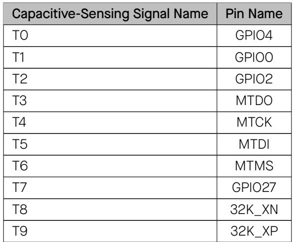
ESP32 has 10 capacitive-sensing GPIOs, which detect variations induced by touching or approaching the GPIOs with a finger or other objects. The low-noise nature of the design and the high sensitivity of the circuit allow relatively small pads to be used. Arrays of pads can also be used, so that a larger area or more points can be detected.
Pin Assignment
The 10 capacitive-sensing GPIOs are listed in Table 11.
Table 11: Capacitive-Sensing GPIOs Available on ESP32
| Capacitive-Sensing Signal Name | Pin Name |
| T0 | GPIO4 |
| T1 | GPIOO |
| T2 | GPIO2 |
| T3 | MTDO |
| T4 | MTCK |
| T5 | MTDI |
| T6 | MTMS |
| T7 | GPIO27 |
| T8 | 32K_XN |
| T9 | 32K_XP |
For details, see ESP32 Technical Reference Manual > Chapter On-Chip Sensors and Analog Signal Processing.
Note: ESP32 Touch Sensor has not passed the Conducted Susceptibility (CS) test for now, and thus has limited application scenarios.
5 Electrical Characteristics
5.1 Absolute Maximum Ratings
Stresses beyond the absolute maximum ratings listed in Table 12 Absolute Maximum Ratings below may cause permanent damage to the device. These are stress ratings only, and do not refer to the functional operation of the device that should follow the Table 13 Recommended Operating Conditions.
Table 12: Absolute Maximum Ratings
| Symbol | Parameter | Min | Max | Unit |
| VDD33 | Power supply voltage | -0.3 | 3.6 | V |
| $I_{output}^{1}$ | Cumulative IO output current | - | 1,100 | mA |
| $T_{store}$ | Storage temperature | -40 | 105 | °C |
- The module worked properly after a 24-hour test in ambient temperature at 25 °C, and the IOs in three domains (VDD3P3_RTC, VDD3P3_CPU, VDD_SDIO) output high logic level to ground. Please note that pins occupied by flash and/or PSRAM in the VDD_SDIO power domain were excluded from the test.
- Please see Appendix IO_MUX of ESP32 Datasheet for IO’s power domain.
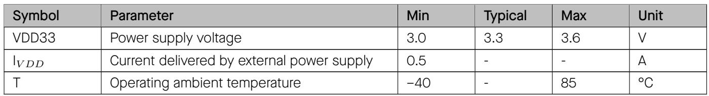
5.2 Recommended Operating Conditions
Table 13: Recommended Operating Conditions
| Symbol | Parameter | Min | Typical | Max | Unit |
| VDD33 | Power supply voltage | 3.0 | 3.3 | 3.6 | V |
| $I_{VDD}$ | Current delivered by external power supply | 0.5 | - | - | A |
| T | Operating ambient temperature | -40 | - | 85 | °C |
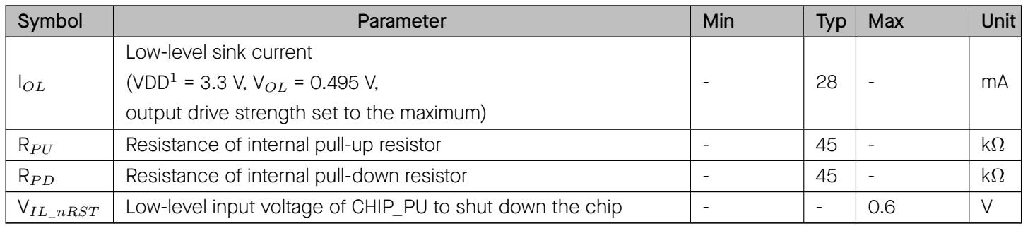
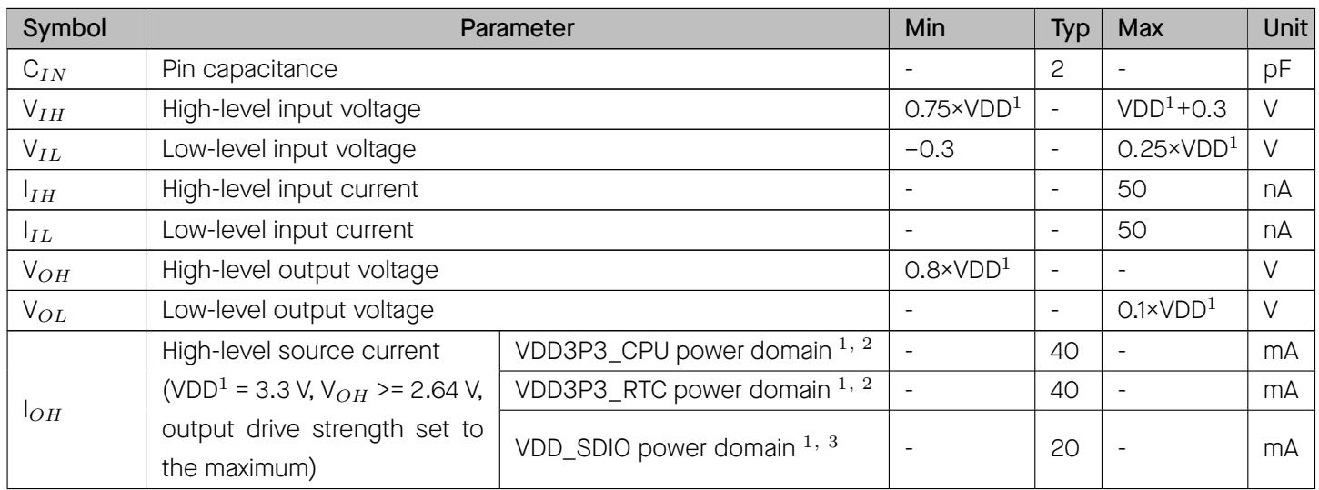
5.3 DC Characteristics (3.3 V, 25 °C)
Table 14: DC Characteristics (3.3 V, 25 °C)
| Symbol | Parameter | Min | Typ | Max | Unit | |
| $C_{IN}$ | Pin capacitance | - | 2 | - | pF | |
| $V_{IH}$ | High-level input voltage | 0.75×VDD1 | - | VDD1+0.3 | V | |
| $V_{IL}$ | Low-level input voltage | -0.3 | - | 0.25×VDD1 | V | |
| $I_{IH}$ | High-level input current | - | - | 50 | nA | |
| $I_{IL}$ | Low-level input current | - | - | 50 | nA | |
| $V_{OH}$ | High-level output voltage | 0.8×VDD1 | - | - | V | |
| $V_{OL}$ | Low-level output voltage | - | - | 0.1×VDD1 | V | |
| $I_{OH}$ | High-level source current(VDD1= 3.3 V, $V_{OH}$ >= 2.64 V,output drive strength set tothe maximum) | VDD3P3_CPU power domain 1, 2 | - | 40 | - | mA |
| VDD3P3_RTC power domain 1, 2 | - | 40 | - | mA | ||
| VDD_SDIO power domain 1, 3 | - | 20 | - | mA | ||
| Symbol | Parameter | Min | Typ | Max | Unit |
| $I_{OL}$ | Low-level sink current( $VDD^1 = 3.3 \text{ V}, V_{OL} = 0.495 \text{ V},$ output drive strength set to the maximum) | - | 28 | - | mA |
| $R_{PU}$ | Resistance of internal pull-up resistor | - | 45 | - | kΩ |
| $R_{PD}$ | Resistance of internal pull-down resistor | - | 45 | - | kΩ |
| $V_{IL\_nRST}$ | Low-level input voltage of CHIP_PU to shut down the chip | - | - | 0.6 | V |
Notes:
- Please see Appendix IO_MUX of ESP32 Datasheet for IO’s power domain. VDD is the I/O voltage for a particular power domain of pins.
- For VDD3P3_CPU and VDD3P3_RTC power domain, per-pin current sourced in the same domain is gradually reduced from around 40 mA to around 29 mA, VOH>=2.64 V, as the number of current-source pins increases.
- Pins occupied by flash and/or PSRAM in the VDD_SDIO power domain were excluded from the test.
5.4 Current Consumption Characteristics
Owing to the use of advanced power-management technologies, the module can switch between different power modes. For details on different power modes, please refer to Section RTC and Low-Power Management in ESP32 Series Datasheet.
5.5 Memory Specifications
The data below is sourced from the memory vendor datasheet. These values are guaranteed through design and/or characterization but are not fully tested in production. Devices are shipped with the memory erased.
Table 15: Flash Specifications
| Parameter | Description | Min | Typ | Max | Unit |
| VCC | Power supply voltage (1.8 V) | 1.65 | 1.80 | 2.00 | V |
| Power supply voltage (3.3 V) | 2.7 | 3.3 | 3.6 | V | |
| $F_C$ | Maximum clock frequency | 80 | — | — | MHz |
| — | Program/erase cycles | 100,000 | — | — | cycles |
| $T_{RET}$ | Data retention time | 20 | — | — | years |
| $T_{PP}$ | Page program time | — | 0.8 | 5 | ms |
| $T_{SE}$ | Sector erase time (4 KB) | — | 70 | 500 | ms |
| $T_{BE1}$ | Block erase time (32 KB) | — | 0.2 | 2 | s |
| $T_{BE2}$ | Block erase time (64 KB) | — | 0.3 | 3 | s |
| $T_{CE}$ | Chip erase time (16 Mb) | — | 7 | 20 | s |
| Chip erase time (32 Mb) | — | 20 | 60 | s | |
| Chip erase time (64 Mb) | — | 25 | 100 | s | |
| Chip erase time (128 Mb) | — | 60 | 200 | s | |
| Chip erase time (256 Mb) | — | 70 | 300 | s |
6 RF Characteristics
This section contains tables with RF characteristics of the Espressif product.
The RF data is measured at the antenna port, where RF cable is connected, including the front-end loss.
Devices should operate in the center frequency range allocated by regional regulatory authorities. The target center frequency range and the target transmit power are configurable by software. See ESP RF Test Tool and Test Guide for instructions.
Unless otherwise stated, the RF tests are conducted with a 3.3 V (±5%) supply at $2 5 ^ { \circ } \mathrm { C }$ ambient temperature.
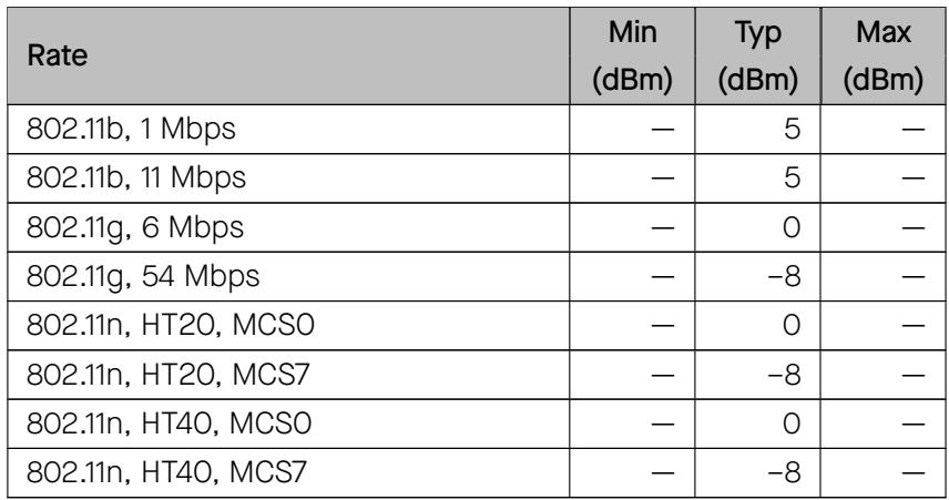
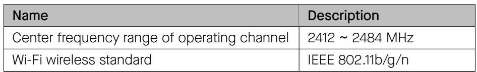
6.1 Wi-Fi Radio
Table 16: Wi-Fi RF Characteristics
| Name | Description |
| Center frequency range of operating channel | 2412 ~ 2484 MHz |
| Wi-Fi wireless standard | IEEE 802.11b/g/n |
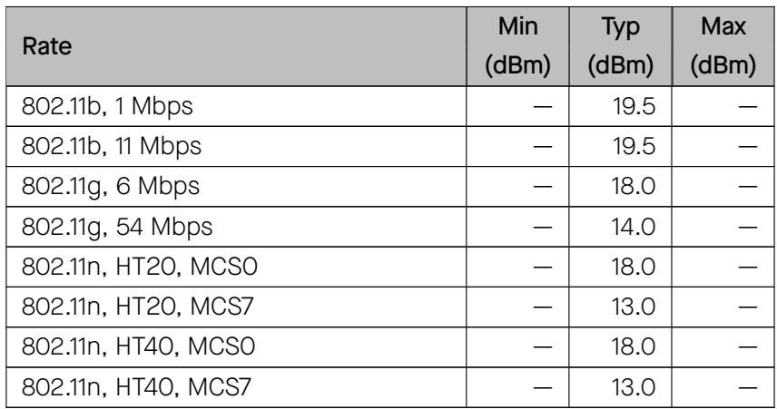
6.1.1 Wi-Fi RF Transmitter (TX) Characteristics
Table 17: TX Power with Spectral Mask and EVM Meeting 802.11 Standards
| Rate | Min (dBm) | Typ (dBm) | Max (dBm) |
| 802.11b, 1 Mbps | — | 19.5 | — |
| 802.11b, 11 Mbps | — | 19.5 | — |
| 802.11g, 6 Mbps | — | 18.0 | — |
| 802.11g, 54 Mbps | — | 14.0 | — |
| 802.11n, HT20, MCS0 | — | 18.0 | — |
| 802.11n, HT20, MCS7 | — | 13.0 | — |
| 802.11n, HT40, MCS0 | — | 18.0 | — |
| 802.11n, HT40, MCS7 | — | 13.0 | — |
Table 18: TX EVM Test1
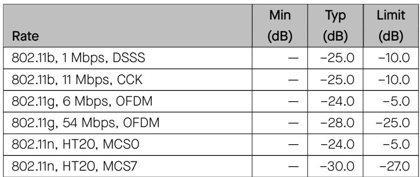
| Rate | Min (dB) | Typ (dB) | Limit (dB) |
| 802.11b, 1 Mbps, DSSS | — | -25.0 | -10.0 |
| 802.11b, 11 Mbps, CCK | — | -25.0 | -10.0 |
| 802.11g, 6 Mbps, OFDM | — | -24.0 | -5.0 |
| 802.11g, 54 Mbps, OFDM | — | -28.0 | -25.0 |
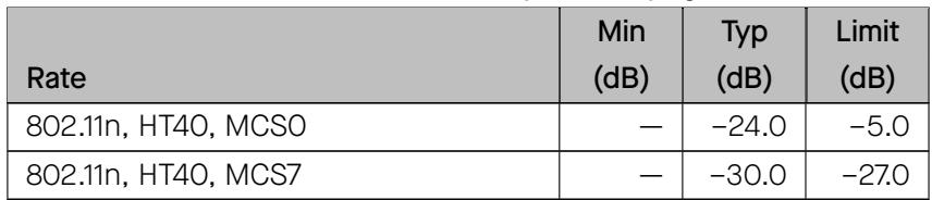
| 802.11n, HT20, MCS0 | — | -24.0 | -5.0 |
| 802.11n, HT20, MCS7 | — | -30.0 | -27.0 |
Cont’d on next page
Table 18 – cont’d from previous page
| Rate | Min (dB) | Typ (dB) | Limit (dB) |
| 802.11n, HT40, MCS0 | — | -24.0 | -5.0 |
| 802.11n, HT40, MCS7 | — | -30.0 | -27.0 |
1 EVM is measured at the corresponding typical TX power provided in Table 17 Wi-Fi RF Transmitter (TX) Characteristics above.
6.1.2 Wi-Fi RF Receiver (RX) Characteristics
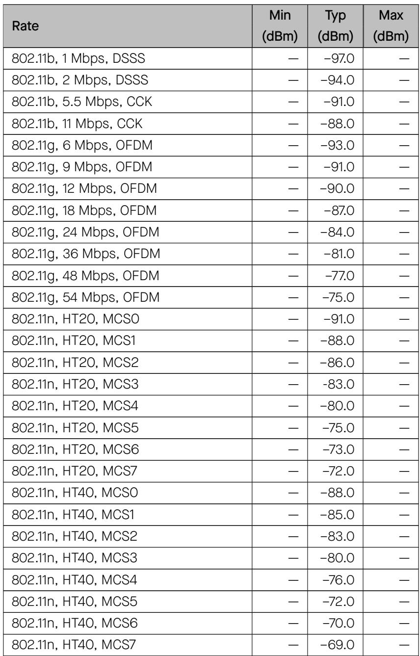
For RX tests, the PER (packet error rate) limit is 8% for 802.11b, and 10% for 802.11g/n.
Table 19: RX Sensitivity
| Rate | Min (dBm) | Typ (dBm) | Max (dBm) |
| 802.11b, 1 Mbps, DSSS | — | -97.0 | — |
| 802.11b, 2 Mbps, DSSS | — | -94.0 | — |
| 802.11b, 5.5 Mbps, CCK | — | -91.0 | — |
| 802.11b, 11 Mbps, CCK | — | -88.0 | — |
| 802.11g, 6 Mbps, OFDM | — | -93.0 | — |
| 802.11g, 9 Mbps, OFDM | — | -91.0 | — |
| 802.11g, 12 Mbps, OFDM | — | -90.0 | — |
| 802.11g, 18 Mbps, OFDM | — | -87.0 | — |
| 802.11g, 24 Mbps, OFDM | — | -84.0 | — |
| 802.11g, 36 Mbps, OFDM | — | -81.0 | — |
| 802.11g, 48 Mbps, OFDM | — | -77.0 | — |
| 802.11g, 54 Mbps, OFDM | — | -75.0 | — |
| 802.11n, HT20, MCS0 | — | -91.0 | — |
| 802.11n, HT20, MCS1 | — | -88.0 | — |
| 802.11n, HT20, MCS2 | — | -86.0 | — |
| 802.11n, HT20, MCS3 | — | -83.0 | — |
| 802.11n, HT20, MCS4 | — | -80.0 | — |
| 802.11n, HT20, MCS5 | — | -75.0 | — |
| 802.11n, HT20, MCS6 | — | -73.0 | — |
| 802.11n, HT20, MCS7 | — | -72.0 | — |
| 802.11n, HT40, MCS0 | — | -88.0 | — |
| 802.11n, HT40, MCS1 | — | -85.0 | — |
| 802.11n, HT40, MCS2 | — | -83.0 | — |
| 802.11n, HT40, MCS3 | — | -80.0 | — |
| 802.11n, HT40, MCS4 | — | -76.0 | — |
| 802.11n, HT40, MCS5 | — | -72.0 | — |
| 802.11n, HT40, MCS6 | — | -70.0 | — |
| 802.11n, HT40, MCS7 | — | -69.0 | — |
Table 20: Maximum RX Level
| Rate | Min (dBm) | Typ (dBm) | Max (dBm) |
| 802.11b, 1 Mbps | — | 5 | — |
| 802.11b, 11 Mbps | — | 5 | — |
| 802.11g, 6 Mbps | — | 0 | — |
| 802.11g, 54 Mbps | — | -8 | — |
| 802.11n, HT20, MCS0 | — | 0 | — |
| 802.11n, HT20, MCS7 | — | -8 | — |
| 802.11n, HT40, MCS0 | — | 0 | — |
| 802.11n, HT40, MCS7 | — | -8 | — |
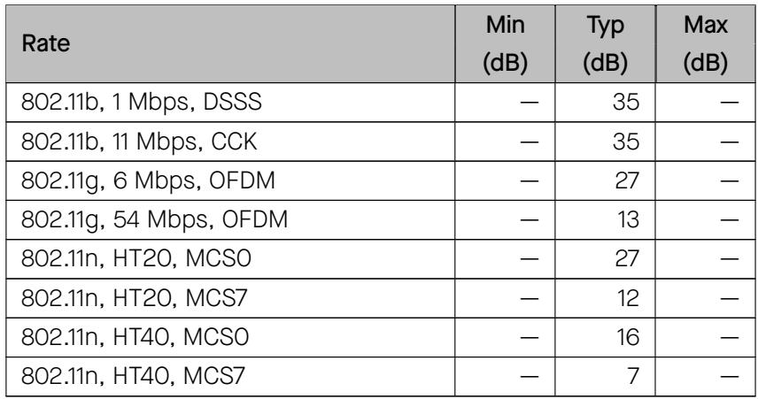
Table 21: RX Adjacent Channel Rejection
| Rate | Min (dB) | Typ (dB) | Max (dB) |
| 802.11b, 1 Mbps, DSSS | — | 35 | — |
| 802.11b, 11 Mbps, CCK | — | 35 | — |
| 802.11g, 6 Mbps, OFDM | — | 27 | — |
| 802.11g, 54 Mbps, OFDM | — | 13 | — |
| 802.11n, HT20, MCS0 | — | 27 | — |
| 802.11n, HT20, MCS7 | — | 12 | — |
| 802.11n, HT40, MCS0 | — | 16 | — |
| 802.11n, HT40, MCS7 | — | 7 | — |
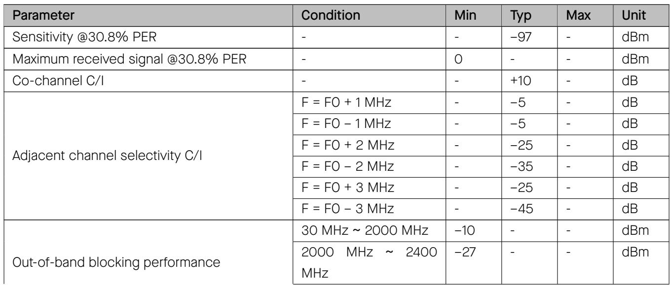
6.2 Bluetooth LE Radio
6.2.1 Receiver
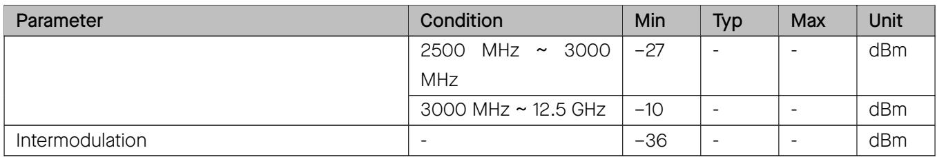
Table 22: Receiver Characteristics – Bluetooth LE
| Parameter | Condition | Min | Typ | Max | Unit |
| Sensitivity @30.8% PER | - | - | -97 | - | dBm |
| Maximum received signal @30.8% PER | - | 0 | - | - | dBm |
| Co-channel C/I | - | - | +10 | - | dB |
| Adjacent channel selectivity C/I | F = F0 + 1 MHz | - | -5 | - | dB |
| F = F0 - 1 MHz | - | -5 | - | dB | |
| F = F0 + 2 MHz | - | -25 | - | dB | |
| F = F0 - 2 MHz | - | -35 | - | dB | |
| F = F0 + 3 MHz | - | -25 | - | dB | |
| F = F0 - 3 MHz | - | -45 | - | dB | |
| Out-of-band blocking performance | 30 MHz ~ 2000 MHz | -10 | - | - | dBm |
| 2000 MHz ~ 2400 MHz | -27 | - | - | dBm | |
| 2500 MHz ~ 3000 MHz | -27 | - | - | dBm | |
| 3000 MHz ~ 12.5 GHz | -10 | - | - | dBm | |
| Intermodulation | - | -36 | - | - | dBm |
6.2.2 Transmitter
Table 23: Transmitter Characteristics – Bluetooth LE
| Parameter | Condition | Min | Typ | Max | Unit |
| RF transmit power | - | - | 0 | - | dBm |
| Gain control step | - | - | 3 | - | dBm |
| RF power control range | - | -12 | - | +9 | dBm |
| Adjacent channel transmit power | F = F0 ± 2 MHz | - | -52 | - | dBm |
| F = F0 ± 3 MHz | - | -58 | - | dBm | |
| F = F0 ± >3 MHz | - | -60 | - | dBm | |
| $\Delta f1_{avg}$ | - | - | - | 265 | kHz |
| $\Delta f2_{max}$ | - | 247 | - | - | kHz |
| $\Delta f2_{avg}/\Delta f1_{avg}$ | - | - | -0.92 | - | - |
| ICFT | - | - | -10 | - | kHz |
| Drift rate | - | - | 0.7 | - | kHz/50 μs |
| Drift | - | - | 2 | - | kHz |
Th is is th e refe re n ce d esi g n of th e m od u l e .
M odu le Schematics
other
| Pin | Value |
|---|---|
| Pin.1 | 1 |
| Pin.2 | 2 |
| Pin.3 | 3 |
| Pin.4 | 4 |
| Pin.5 | 5 |
| Pin.6 | 6 |
| Pin.7 | 7 |
| Pin.8 | 8 |
| Pin.9 | 9 |
| Pin.10 | 10 |
| Pin.11 | 11 |
| Pin.12 | 12 |
| Pin.13 | 13 |
| Pin.14 | 14 |
| Pin.15 | 15 |
| Pin.16 | 16 |
| Pin.17 | 17 |
| Pin.18 | 18 |
| Pin.19 | 19 |
| Pin.20 | 20 |
| Pin.21 | 21 |
| Pin.22 | 22 |
| Pin.23 | 23 |
| Pin.24 | 24 |
| Pin.25 | 25 |
| Pin.26 | 26 |
| Pin.27 | 27 |
| Pin.28 | 28 |
| Pin.29 | 29 |
| Pin.30 | 30 |
| Pin.31 | 31 |
| Pin.32 | 32 |
| Pin.33 | 33 |
| Pin.34 | 34 |
| Pin.35 | 35 |
| Pin.36 | 36 |
| Pin.37 | 37 |
| Pin.38 | 38 |
| The values of C14, L4 and C15 vary with the actual selection of a PCB board. |
Figu re 5: ESP32-WROO M -32 Schematics
8 Peripheral Schematics
This is the typical application circuit of the module connected with peripheral components (for example, power supply, antenna, reset button, JTAG interface, and UART interface).
text_image
VDD33 VDD33
C1 10uF
C2 0.1uF
GND
R1
TBD
EN
GND
U1
GND1
2
3
4
5
6
7
8
9
10
11
12
13
14
15
16
17
18
19
20
21
22
23
24
P_GND
39
38
37
IO23
36
IO22
35
TXD
34
RXD
33
IO21
32
NC
31
IO19
30
IO18
29
IO5
28
IO17
27
IO16
26
IO4
25
IO0
GND2
GND3
I023
I022
I021
I019
I018
I017
I016
I015
I014
I013
SD2 SD3 CMD CLK SD0 SD1 IO2
SD3 SD4 CLK SD0 SD1 IO2
MTDI should be kept at a low electric level when powering up the module.
MTDI should be kept at a low electric level when powering up the module.
MTCK 100R MTMS 4 R2 R3 R4 R5 MTDO MTDO JTAG U2 BOOT OPTION
Figure 6: ESP32-WROOM-32 Peripheral Schematics
Soldering Pad 39 to the ground of the base board is not a must. If you choose to solder it, please apply Espressifthe correct amount of soldering paste. Too much soldering paste may increase the gap between the Title Appmodule and the baseboard. As a result, the adhesion between other pins and the baseboard may be poor.
Date: Wed To ensure the power supply to the ESP32 chip during power-up, it is advised to add an RC delay circuit at the EN pin. The recommended setting for the RC delay circuit is usually R = 10 kΩ and C = 1 µF. However, specific parameters should be adjusted based on the power-up timing of the module and the power-up and reset sequence timing of the chip. For ESP32’s power-up and reset sequence timing diagram, please refer to Section 3.6 Chip Power-up and Reset.
• UART0 is used to download firmware and log output. When using the AT firmware, note that the UART GPIO is already configured. It is recommended to use the default configuration. Please refer to ESP-AT User Guide for ESP32 > Section Hardware Connection.
9 Module Dimensions
text_image
25.50±0.15
0.45
0.90
16.51
1.50
1.27
1.05
8.89
11.43
17.60
15.80
Ø1.00
18.00±0.15
5.94
Top View
text_image
3.10±0.15
0.80
0.1
Side View
Unit: mm
text_image
0.85
0.90
0.90
0.85
5.94
4.10
4.10
9.68
10.67
Bottom View
Figure 7: Physical Dimensions
Note:
For information about tape, reel, and product marking, please refer to ESP32 Module Packaging Information.
10 PCB Layout Recommendations
10.1 PCB Land Pattern
This section provides the following resources for your reference:
• Figures for recommended PCB land patterns with all the dimensions needed for PCB design. See Figure 10.1 PCB Land Pattern.
Source files of recommended PCB land patterns to measure dimensions not covered in Figure 10.1. You can view the source files for ESP32-WROOM-32 with Autodesk Viewer.
other
| Dimension | Value |
|---|---|
| Total Height | 18.00 |
| Diameter | 5.94 |
| Thickness | 38x1.50 |
| Width | 38x0.90 |
| Thickness | 25.50 |
| Width | 1.50 |
| Thickness | 1.27 |
| Width | 1.27 |
| Thickness | 1.43 |
| Width | 10.67 |
| Thickness | 8.32 |
| Width | 1.05 |
| Thickness | 0.475 |
| Width | 1.05 |
| Thickness | 1.05 |
| Width | 4.10 |
| Thickness | 4.10 |
| Width | 1.50 |
| Thickness | 24 |
| Width | 25 |
| Thickness | 24 |
| Width | 11.43 |
| Thickness | 11.43 |
| Width | 0.50 |
| Thickness | 0.50 |
| Width | 3.28 |
| Unit: mm |
Figure 8: Recommended PCB Land Pattern
10.2 Module Placement for PCB Design
If module-on-board design is adopted, attention should be paid while positioning the module on the base board. The interference of the base board on the module’s antenna performance should be minimized.
For details about module placement for PCB design, please refer to ESP32 Hardware Design Guidelines > Section General Principles of PCB Layout for Modules.
11 Product Handling
11.1 Storage Conditions
The products sealed in moisture barrier bags (MBB) should be stored in a non-condensing atmospheric environment of $< 4 0 ~ ^ { \circ } \mathrm { C }$ and 90%RH. The module is rated at the moisture sensitivity level (MSL) of 3.
After unpacking, the module must be soldered within 168 hours with the factory conditions $2 5 \pm 5 ^ { \circ } \mathrm { C }$ and 60 %RH. If the above conditions are not met, the module needs to be baked.
11.2 Electrostatic Discharge (ESD)
Human body model (HBM): ±2000 V
• Charged-device model (CDM): ±500 V
11.3 Reflow Profile
Solder the module in a single reflow.
line
| Phase | Temperature (°C) |
|---|---|
| Ramp-up zone | 1 ~ 3 °C/s |
| Preheating zone | 150 ~ 200 °C |
| Reflow zone | >217 °C |
| Peak Temp. | 235 ~ 250 °C |
| Solder | -1 ~ -5 °C/s |
Figure 9: Reflow Profile
11.4 Ultrasonic Vibration
Avoid exposing Espressif modules to vibration from ultrasonic equipment, such as ultrasonic welders or ultrasonic cleaners. This vibration may induce resonance in the in-module crystal and lead to its malfunction or even failure. As a consequence, the module may stop working or its performance may deteriorate.
Datasheet Versioning
| Datasheet Version | Status | Watermark | Definition |
| v0.1 ~ v0.5 (excluding v0.5) | Draft | Confidential | This datasheet is under development for products in the design stage. Specifications may change without prior notice. |
| v0.5 ~ v1.0 (excluding v1.0) | Preliminary release | Preliminary | This datasheet is actively updated for products in the verification stage. Specifications may change before mass production, and the changes will be documentation in the datasheet's Revision History. |
| v1.0 and higher | Official release | — | This datasheet is publicly released for products in mass production. Specifications are finalized, and major changes will be communicated viaProduct Change Notifications (PCN). |
| Any version | — | Not Recommended for New Design (NRND) $^{1}$ | This datasheet is updated less frequently for products not recommended for new designs. |
| Any version | — | End of Life (EOL) $^{2}$ | This datasheet is no longer mtained for products that have reached end of life. |
1 Watermark will be added to the datasheet title page only when all the product variants covered by this datasheet are not recommended for new designs.
2 Watermark will be added to the datasheet title page only when all the product variants covered by this datasheet have reached end of life.
Related Documentation and Resources
Related Documentation
ESP32 Series Datasheet – Specifications of the ESP32 hardware.
ESP32 ECO and Workarounds for Bugs – Correction of ESP32 design errors.
ESP32 Series SoC Errata – Descriptions of known errors in ESP32 series of SoCs.
Certificates https://espressif.com/en/support/documents/certificates
ESP32 Technical Reference Manual – Detailed information on how to use the ESP32 memory and peripherals.
• ESP32 Hardware Design Guidelines – Guidelines on how to integrate the ESP32 into your hardware product.
• ESP32 Product/Process Change Notifications (PCN) https://espressif.com/en/support/documents/pcns
• ESP32 Advisories – Information on security, bugs, compatibility, component reliability. https://espressif.com/en/support/documents/advisories
Documentation Updates and Update Notification Subscription https://espressif.com/en/support/download/documents
Developer Zone
ESP-IDF Programming Guide for ESP32 – Extensive documentation for the ESP-IDF development framework.
ESP-IDF and other development frameworks on GitHub. https://github.com/espressif
• ESP32 BBS Forum – Engineer-to-Engineer (E2E) Community for Espressif products where you can post questions, share knowledge, explore ideas, and help solve problems with fellow engineers. https://esp32.com/
ESP-FAQ – A summary document of frequently asked questions released by Espressif. https://espressif.com/projects/esp-faq/en/latest/index.html
The ESP Journal – Best Practices, Articles, and Notes from Espressif folks. https://blog.espressif.com/
See the tabs SDKs and Demos, Apps, Tools, AT Firmware. https://espressif.com/en/support/download/sdks-demos
Products
ESP32 Series SoCs – Browse through all ESP32 SoCs. https://espressif.com/en/products/socs?id=ESP32
ESP32 Series Modules – Browse through all ESP32-based modules. https://espressif.com/en/products/modules?id=ESP32
ESP32 Series DevKits – Browse through all ESP32-based devkits. https://espressif.com/en/products/devkits?id=ESP32
• ESP Product Selector – Find an Espressif hardware product suitable for your needs by comparing or applying filters. https://products.espressif.com/#/product-selector?language=en
Contact Us
See the tabs Sales Questions, Technical Enquiries, Circuit Schematic & PCB Design Review, Get Samples (Online stores), Become Our Supplier, Comments & Suggestions. https://espressif.com/en/contact-us/sales-questions
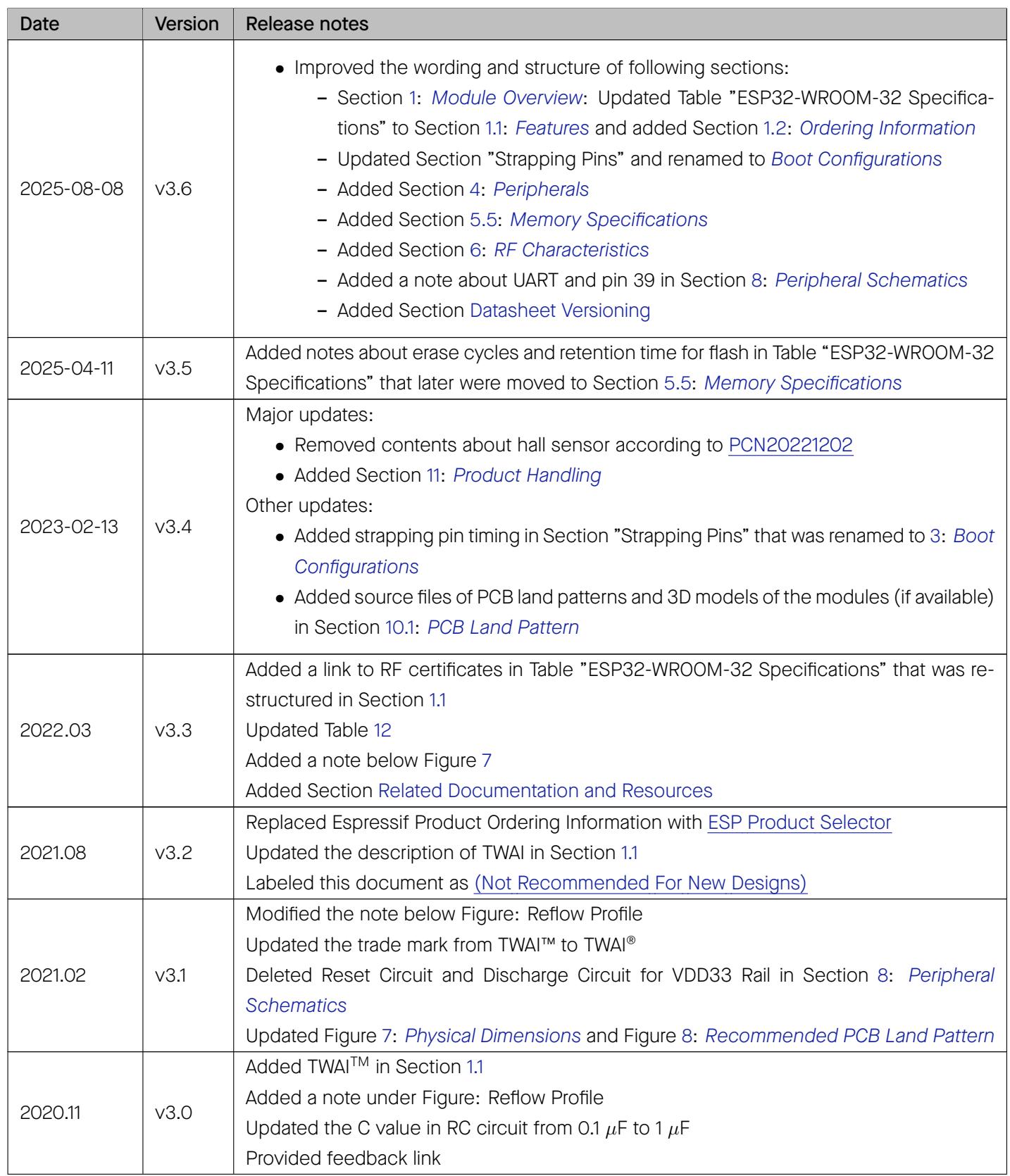
Revision History
| Date | Version | Release notes |
| 2025-08-08 | v3.6 | Improved the wording and structure of following sections:Section 1:Module Overview: Updated Table "ESP32-WROOM-32 Specifications" to Section 1.1:Features and added Section 1.2:Ordering InformationUpdated Section "Strapping Pins" and renamed toBoot ConfigurationsAdded Section 4:PeripheralsAdded Section 5.5:Memory SpecificationsAdded Section 6:RF CharacteristicsAdded a note about UART and pin 39 in Section 8:Peripheral SchematicsAdded Section Datasheet Versioning |
| 2025-04-11 | v3.5 | Added notes about erase cycles and retention time for flash in Table "ESP32-WROOM-32 Specifications" that later were moved to Section 5.5:Memory Specifications |
| 2023-02-13 | v3.4 | Major updates:Removed contents about hall sensor according toPCN20221202Added Section 11:Product HandlingOther updates:Added strapping pin timing in Section "Strapping Pins" that was renamed to 3:Boot ConfigurationsAdded source files of PCB land patterns and 3D models of the modules (if available) in Section 10.1:PCB Land Pattern |
| 2022.03 | v3.3 | Added a link to RF certificates in Table "ESP32-WROOM-32 Specifications" that was restructured in Section 1.1Updated Table 12Added a note below Figure 7Added Section Related Documentation and Resources |
| 2021.08 | v3.2 | Replaced Espressif Product Ordering Information withESP Product SelectorUpdated the description of TWAI in Section 1.1Labeled this document as(Not Recommended For New Designs) |
| 2021.02 | v3.1 | Modified the note below Figure: Reflow ProfileUpdated the trade mark from TWAI $^{\text{TM}}$ to TWAI $^{\text{®}}$ Deleted Reset Circuit and Discharge Circuit for VDD33 Rail in Section 8:Peripheral SchematicsUpdated Figure 7:Physical Dimensions and Figure 8:Recommended PCB Land Pattern |
| 2020.11 | v3.0 | Added TWAI $^{\text{TM}}$ in Section 1.1Added a note under Figure: Reflow ProfileUpdated the C value in RC circuit from 0.1 $\mu$ F to 1 $\mu$ FProvided feedback link |
| 2019.09 | v2.9 | Changed the supply voltage range from 2.7 V ~ 3.6 V to 3.0 V ~ 3.6 VAdded Moisture sensitivity level (MSL) 3 in Table "ESP32-WROOM-32 Specifications"Added notes about "Operating frequency range" and "TX power" under Table "WiFi Radio Characteristics" that was restructured in several tables in Section 6: RF CharacteristicsUpdated Section 8 Peripheral Schematics and added a note about RC delay circuit under itUpdated Figure 8 Recommended PCB Land Pattern |
| 2019.01 | v2.8 | Changed the RF power control range in Table 23 from -12 ~ +12 to -12 ~ +9 dBm |
| 2018.10 | v2.7 | Added "Cumulative IO output current" entry to Table 12: Absolute Maximum Ratings Added more parameters to Table 14: DC Characteristics (3.3 V, 25 °C) |
| 2018.08 | v2.6 | Added reliability test items the module has passed in Table "ESP32-WROOM-32 Specifications", and removed software-specific informationUpdated section "RTC and Low-Power Management" that was renamed as 5.4: Current Consumption CharacteristicsChanged the module's dimensions from (18±0.2) mm x (25.5 ±0.2) mm x (3.1±0.15) mm to (18.00±0.10) mm x (25.50±0.10) mm x (3.10±0.10) mmUpdated Figure 7: Physical DimensionsUpdated Table "Wi-Fi Radio Characteristics" that was restructured in several tables in Section 6: RF Characteristics |
| 2018.06 | v2.5 | Changed the module name to ESP32-WROOM-32Deleted Temperature Sensor in Table "ESP32-WROOM-32 Specifications"Updated Chapter "Functional Description" (later updated to Section 4: Peripherals)Added Chapter 10.1: PCB Land PatternChanges to electrical characteristics:Updated Table 12: Absolute Maximum RatingsAdded Table 13: Recommended Operating ConditionsAdded Table 14: DC Characteristics (3.3 V, 25 °C)Updated the values of "Gain control step", "Adjacent channel transmit power" in Table 23: Transmitter Characteristics - BLE |
| 2018.03 | v2.4 | Updated Table "ESP32-WROOM-32 Specifications" |
| 2018.01 | v2.3 | Deleted information on LNA pre-amplifierUpdated Section "RTC and Low-Power Management" that was renamed as 5.4: Current Consumption CharacteristicsAdded reset circuit in Chapter 8 and a note to it |
| 2017.10 | v2.2 | Updated the description of the chip's system reset in Section "Strapping Pins"Deleted "Association sleep pattern" in Table "Power Consumption by Power Modes" and added notes to Active sleep and Modem-sleepUpdated the note to Figure 6 Peripheral SchematicsAdded discharge circuit for VDD33 rail in Chapter 8 and a note to it |
| 2017.09 | v2.1 | Updated operating voltage/power supply range updated to 2.7 ~ 3.6 VUpdated Chapter 8 |
| 2017.08 | v2.0 | Changed the sensitivity of NZIF receiver to -97 dBm in Table "ESP32-WROOM-32 Specifications"Updated the dimensions of the moduleUpdated Table "Power Consumption by Power Modes" Power Consumption by Power Modes, and added two notes to itUpdated Table 12, Table "Wi-Fi Radio Characteristics", 22, 23Added Chapter 9Added the link to Certification Download |
| 2017.06 | v1.9 | Added a note to Section 2.1 Pin LayoutUpdated Section "Crystal Oscillators"Updated Figure 5 ESP-WROOM-32 SchematicsAdded Documentation Change Notification |
| 2017.05 | v1.8 | Updated Figure 1 Top and Side View of ESP32-WROOM-32 (ESP-WROOM-32) |
| 2017.04 | v1.7 | Added the module's dimensional toleranceChanged the input impedance value of 50 Ω in Table "Wi-Fi Radio Characteristics" (restructured in several tables in Section 6: RF Characteristics) to output impedance value of 30+j10 Ω |
| 2017.04 | v1.6 | Added Figure: Reflow Profile |
| 2017.03 | v1.5 | Updated Section 2.2 Pin DescriptionUpdated Section "External Flash and SRAM"Updated Section "Peripherals and Sensors Description" |
| 2017.03 | v1.4 | Updated PrefaceUpdated Chapter 2 Pin DefinitionsUpdated Chapter "Functional Description"Updated Table Recommended Operating ConditionsUpdated Table "Wi-Fi Radio Characteristics"Updated Section: Reflow ProfileAdded Chapter Learning Resources |
| 2016.12 | v1.3 | Updated Section 2.1 Pin Layout |
| 2016.11 | v1.2 | Added Figure 6 Peripheral Schematics |
| 2016.11 | v1.1 | Updated Chapter 8 Schematics |
| 2016.08 | v1.0 | First release |

ESPRESSIF
Disclaimer and Copyright Notice
Information in this document, including URL references, is subject to change without notice.
ALL THIRD PARTY’S INFORMATION IN THIS DOCUMENT IS PROVIDED AS IS WITH NO WARRANTIES TO ITS AUTHENTICITY AND ACCURACY.
NO WARRANTY IS PROVIDED TOTHIS DOCUMENT EORITS MERCHANTABILITY NON-INERINGEMENI,FITNESS FOR ANYPARTICULAR PURPOSE, NOR DOES ANY WARRANTY OTHERWISE ARISING OUT OF ANY PROPOSAL, SPECIFICATION OR SAMPLE.
All liability, including liability for infringement of any proprietary rights, relating to use of information in this document is disclaimed. No licenses express or implied, by estoppel or otherwise, to any intellectual property rights are granted herein.
The Wi-Fi Alliance Member logo is a trademark of the Wi-Fi Alliance. The Bluetooth logo is a registered trademark of Bluetooth SIG.
All trade names, trademarks and registered trademarks mentioned in this document are property of their respective owners, and are hereby acknowledged.
Copyright © 2025 Espressif Systems (Shanghai) Co., Ltd. All rights reserved.
Extracted Images
Figures and diagrams from the PDF
Preview the extracted datasheet assets and open any image in a separate tab for closer inspection.
Pin definition table for IO22, IO23, and GND
Revision history table
RF transmitter characteristics table
Recommended operating conditions table
802.11n HT40 modulation characteristics table
Application circuit schematic for ESP32 module
Table of power supply voltage, clock frequency, and erase/program timing specifications
Ordering information table for ESP32-WROOM-32 module
Application schematic for ESP32-D0WDQ6 showing crystal oscillator and pin connections
Pin definition table for ESP32 module
Timing parameters for chip power-up and reset
Mapping table for capacitive-sensing signals to pin names
Strapping pin default configuration and bit values
Boot mode selection based on GPIO strapping pins
Wi-Fi transmission rate limits and typical values
Espressif Systems logo
Intermodulation and frequency range electrical parameters
Power-up and reset timing diagram
Timing parameters for CHIP_PU and strapping pins
ADC linearity and sampling rate specifications
IO and CHIP_PU electrical characteristics
Datasheet versioning and status definitions
Revision history and release notes
RF transmit power specifications by rate
Wi-Fi wireless standard and frequency range specifications
Not Recommended for New Designs (NRND) watermark
Receiver sensitivity and blocking performance table
Edge behavior configuration for MTDO and GPIO5
U0TXD Printing Control configuration via MTDO
Recommended PCB footprint and antenna area dimensions
Side view package drawing with dimensions
Top view package drawing with antenna and dimensions
Absolute maximum ratings table
Wi-Fi radio characteristics table (dB)
Revision history table
Wi-Fi transmit power characteristics table (dBm)
Total error measurement range table
Receiver sensitivity table for various Wi-Fi rates
Mechanical dimensions of the package
Timing diagram for CHIP_PU and strapping pin
Reset and boot sequence flow diagram
Projection symbol or mechanical icon
DC electrical characteristics table showing input/output voltage and current specifications
Reflow soldering temperature profile graph
Top view pinout diagram of a module with keepout zone
QR code snippet
Agent APIs
Use this datasheet from any agent
Send the page, markdown, chunks, or search endpoint to ChatGPT, Claude, embedr-app, or your own tooling.
Original PDF
https://www.embedr.app/api/datasheets/ds_82796e9d0f47b1a24814/pdf
Full Markdown
https://www.embedr.app/api/datasheets/ds_82796e9d0f47b1a24814/markdown
Ordered Chunks
https://www.embedr.app/api/datasheets/ds_82796e9d0f47b1a24814/chunks
Search API
https://www.embedr.app/api/datasheets/ds_82796e9d0f47b1a24814/search
Metadata
https://www.embedr.app/api/datasheets/ds_82796e9d0f47b1a24814/metadata