
NBM7100A/B
Coin cell battery life booster with adaptive power optimization for primary battery-powered, low-power applications with burst current loads.
1. General description
The NBM7100A/B is a battery energy management device designed to maximize usable capacity from non-rechargeable, primary batteries when used in low-voltage, low-power applications requiring burst current loads. The devices overcome voltage drop and battery life limitations associated with extracting high pulse currents (Fig. 1) from lithium primary batteries such as 3 V lithium manganese dioxide (LiMnO $_{2}$ ) coin cells. which are commonly used in wireless, low-power IoT sensor applications.
The NBM7100A/B contains two stages of high efficiency DC-DC conversion and an intelligent learning algorithm. The first stage DC-DC conversion transfers energy from the lithium battery at a low constant current to a capacitive storage element. Once charged, a second DC-DC conversion cycle utilizes this stored energy to supply a regulated voltage with high pulse load current capability on the VDH output pin. The battery is never directly subjected to large load pulse currents, resulting in a longer, more predictable battery lifetime.
The proprietary learning algorithm monitors the energy used during repetitive load pulse cycles and optimizes first stage DC-DC conversion to minimize the residual charge in the storage capacitor.
A serial interface allows a microcontroller to change default configuration settings and read-back system information.
Table 1. Related devices
| Type number | Bus interface | Auto start | Pulse $I_{LOAD}$ |
| NBM7100A | $I^{2}C$ | Yes | $\geq 200 mA$ |
| NBM7100B | SPI | No | $\geq 200 mA$ |
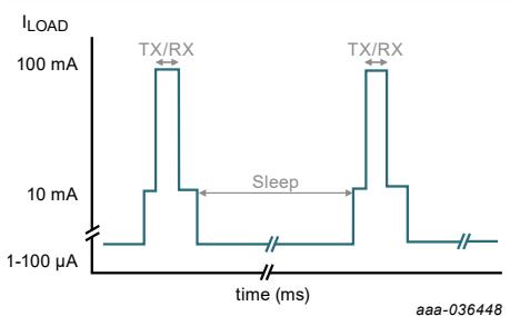
Fig. 1. IoT pulsed load profile
2. Features and benefits
- Programmable constant battery load current: 2 mA to 16 mA
• Protection against battery voltage dips (Brown-out)
• Pulse output current: > 200 mA
- Low ripple regulated programmable output voltage, VDH: 1.8 V to 3.6 V
• Ultra-low standby current: 20 nA (typ)
- Peak conversion efficiency up to 93% with adaptive optimization
- Integrated fuel gauge
- Small 16 pin lead-free package (SOT763-1/DHVQFN16; 2.5 mm × 3.5 mm × 0.85 mm)
• Specified from -40 °C to +85 °C
3. Applications
- Battery powered wireless microcontroller applications (IoT): Bluetooth®, LoRaWAN®, Sigfox™, LTE-M, NB-IoT, Zigbee, etc.
- Industrial: temperature, occupancy, e-metering, electronic shelf label, asset tracking, irrigation monitoring
- Consumer/wearable: location tags, heart rate monitor, blood glucose meter, remote controls, key fobs
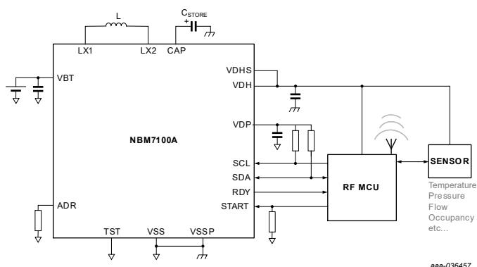
Fig. 2. Simplified Application
Coin cell battery life booster with adaptive power optimization
4. Ordering information
Table 2. Ordering information
| Type number | Package | |||
| Temperature range | Name | Description | Version | |
| NBM7100ABQ | -40 °C to +85 °C | DHVQFN16 | plastic dual in-line compatible thermal enhanced very thin quad flat package; no leads; 16 terminals; body $2.5 \times 3.5 \times 0.85$ mm | SOT763-1 |
| NBM7100BBQ | ||||
5. Marking
Table 3. Marking codes
| Type number | Marking code |
| NBM7100ABQ | M7100A |
| NBM7100BBQ | M7100B |
6. Pin configuration and description
6.1. Pin configuration
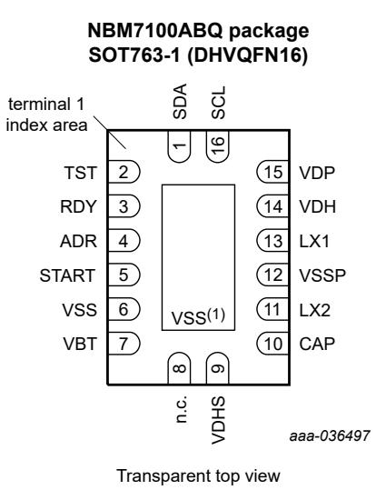
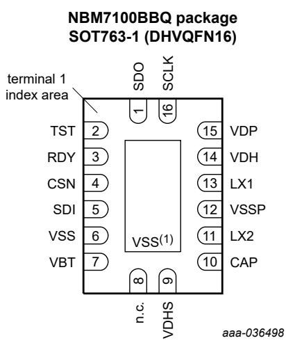
(1) Ground pad should be connected to the analog ground pin VSS.
Fig. 3. Pin configuration SOT763-1 (DHVQFN16)
Coin cell battery life booster with adaptive power optimization
6.2. Pin description
Table 4. Pin description
| Pin | Symbol | I/O | Description | |
| NBM7100A | NBM7100B | |||
| 1 | SDA | SDO | I (A) O (B) | serial data I/O (I2C) / serial data out MISO (SPI) |
| 2 | TST | I | factory test only, tie to VSS | |
| 3 | RDY | O | status output | |
| 4 | ADR | CSN | I | address pin (I2C) / chip select (SPI; active LOW) |
| 5 | START | SDI | I | start pin (active high) [1] / serial data in MOSI (SPI) |
| 6 | VSS | PWR | analog ground, should be connected to VSSP on PCB | |
| 7 | VBT | PWR | input supply to the IC (typically from a battery). | |
| 8 | n.c. | n.a. | not internally connected. connect to PCB pad. | |
| 9 | VDHS | I | sense input | |
| 10 | CAP | PWR | storage capacitor | |
| 11 | LX2 | - | inductor connection 2 | |
| 12 | VSSP | PWR | power (switching) ground, should be connected to VSS on PCB | |
| 13 | LX1 | - | inductor connection 1 | |
| 14 | VDH | O | regulated supply output (see output configuration) | |
| 15 | VDP | O | permanent supply output (see output configuration) | |
| 16 | SCL | SCLK | I | serial clock input SCL (I2C); SCLK (SPI) |
| - | Pad | - | this is not a supply pin; should be soldered to PCB and connected to VSS externally; used to heat-sink the device to the circuit board. | |
[1] Connect to VSS with a pull-down resistor when not actively driving.
Coin cell battery life booster with adaptive power optimization
7. Specifications
7.1. Limiting values
Table 5. Limiting values
In accordance with the Absolute Maximum Rating System (IEC 60134). Voltages are referenced to GND (ground = 0 V).
| Symbol | Parameter | Conditions | Min | Max | Unit |
| $V_{VBT}$ | supply voltage pin VBT | -0.3 | 6.0 | V | |
| $V_I$ | input voltage | VDHSNBM7100A: ADR, START, SCL, SDANBM7100B: CSN, SDI, SDO and SCLK | -0.3 | $V_{VDP}+0.3$ | V |
| $V_O$ | output voltage | VDH and VDP | -0.3 | 6.0 | V |
| $V_{CAP}$ | storage voltage pin CAP | -0.3 | 12.0 | V | |
| $I_O$ | output current | VDH, LX1, LX2 and CAP | - | 500 | mA |
| $T_{amb}$ | ambient temperature | -40 | +85 | °C | |
| $T_{stg}$ | storage temperature | -65 | +150 | °C |
7.2. ESD ratings
Table 6. ESD ratings
| Value | Unit | |||
| $V_{ESD}$ | electrostatic discharge voltage | HBM: ANSI/ESDA/JEDEC JS-001 Class 2 | ± 2000 | V |
| CDM: ANSI/ESDA/JEDEC JS-002 Class C2a | ± 500 | V |
7.3. Thermal information
Table 7. Thermal information
Thermal resistance according to JEDEC51-5 and -7
| Symbol | Parameter | SOT763-1 | Unit |
| $R_{\Theta JA}$ | junction-to-ambient thermal resistance | 82 | K/W |
| $R_{\Theta JC(TOP)}$ | junction-to-case (top) thermal resistance | 50 | K/W |
| $\Psi_{JT}$ | junction-to-top characterization parameter | 7 | K/W |
7.4. Recommended operating conditions
Table 8. Recommended operating conditions
Voltages are referenced to GND (ground = 0 V).
| Symbol | Parameter | Conditions | Min | Max | Unit |
| $V_{VBT}$ | supply voltage | VBT pin | 2.4 | 3.6 | V |
| $V_{I/O}$ | input/output voltage | RDYNBM7100A: SCL, SDA, START, ADRNBM7100B: CSN, SDI, SDO, SCLK | 0 | $V_{VDP}$ | V |
| $I_O$ | output current | VDP pin (Standby state) | 0 | 5 | mA |
| $I_O$ | output current | VDH pin (Active state) | 0 | 200 | mA |
Coin cell battery life booster with adaptive power optimization
7.5. Recommended components
Table 9. Recommended components
Nominal component values, not including tolerance or derating factors. [1]
| Symbol | Parameter | Min | Nom | Max | Unit |
| $C_{VBT}$ | capacitance on VBT | 1 | 2 | - | μF |
| $C_{VDP}$ | capacitance on VDP | 1 | 2 | - | μF |
| $C_{VDH}$ | capacitance on VDH | 22 | - | - | μF |
| $C_{CAP}$ | energy storage capacitance | 4.7 | - | 470 | μF |
| L [2] | inductance between LX1 and LX2 | - | 15 [3] | - | μH |
[1] Nominal component values shown - does not include derating factors.
[2] Ensure inductor saturation current, $I_{SAT}$ , rating > 1 A.
[3] Assume ± 20% tolerance.
7.6. Electrical characteristics
Table 10. Static characteristics
At recommended operating conditions; voltages are referenced to GND (ground = 0 V); typical values are at $25^{\circ}$ C (unless otherwise noted).
$V_{VBT} = 3.0 , V; C_{VBT} = 1 , \mu F; C_{VDP} = 1 , \mu F; C_{VDH} = 22 , \mu F; L = 15 , \mu H;$ unless otherwise specified.
| Symbol | Parameter | Conditions | $T_{amb} = -40 °C to +85 °C$ | Unit | ||
| Min | Typ | Max | ||||
| Input | ||||||
| $V_{POR}$ | power on reset | Device starting voltage for operation at battery insert $T_A = -40 °C$ | 1.3 | - | 2.7 | V |
| $V_{POR}$ | power on reset | Device starting voltage for operation at battery insert $25 °C ≤ T_A ≤ 85 °C$ | 1.3 | - | 2.3 | V |
| $\varepsilon_V$ | absolute voltage error | $V_{FIX}, V_{CAP(max)}, V_{SET}, and V_{EW}$ | - | - | 5 | % |
| Capacitor charge current from VBT pin | ||||||
| $I_{CH}$ | charge current | Charge state, $ich= 000b$ | 1.4 | 2.0 | 2.6 | mA |
| Charge state, $ich= 001b$ | 2.8 | 4.0 | 5.2 | mA | ||
| Charge state, $ich= 010b$ | 5.6 | 8.0 | 10.4 | mA | ||
| Charge state, $ich= 011b$ | 11.2 | 16 | 20.75 | mA | ||
| Charge state, $ich= 100b (V_{CAP} > V_{VBT})$ | 35 | 50 | 85 | mA | ||
| $EFF_{ch}$ | converter efficiency | Conversion efficiency (Charge state) | - | 80 | - | % |
| Supply current from VBT pin | ||||||
| $I_{Q\_STB}$ | quiescent current | Standby state | - | 20 | - | nA |
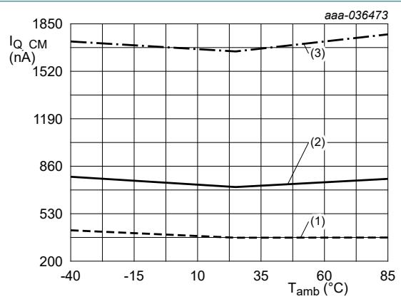
| $I_{Q\_CM}$ | quiescent current | Continuous mode, $C_{STORE}$ charged | - | 1.8 | - | μA |
| $I_{Q\_ACT}$ | quiescent current | Active state, $I_{LOAD}= 10 mA$ | - | 0.4 | - | mA |
Coin cell battery life booster with adaptive power optimization
| Symbol | Parameter | Conditions | $T_{amb} = -40 °C to +85 °C$ | Unit | ||
| Min | Typ | Max | ||||
| VDH output | ||||||
| $V_O$ | output voltage | Active state, $I_{VDH} > 1 mA$ | - | $V_{SET}$ | - | V |
| $\Delta V_{DH(ΔIO)}$ | VDH load regulation | see Fig. 12 | - | ±1 | - | % |
| $EFF_{ACT}$ | converter efficiency | Active state | - | 90 | - | % |
| $R_{VDP}$ | output resistance | pin VDP | - | 20 | 30 | Ω |
| No load detection | ||||||
| No load detection is active in the Auto mode only. It set the device into standby state when the load current is below the threshold $I_{NL}$ for more the $T_{NL}$ .The detected load detection current is the sum of currents in the VDP and VDH outputs. | ||||||
| $I_{NL}$ | threshold current | No load Current threshold | - | 100 | - | μA |
| $T_{NL}$ | detection time | No load Detection time | - | 20 | - | ms |
Table 11. Logic inputs/outputs (SDA/SDO), RDY, (ADR/CSN), (START/SDI) and (SCL/SCLK) pins
At recommended operating conditions; voltages are referenced to GND (ground = 0 V); typical values are at $25^{\circ}$ C (unless otherwise noted).
$V_{VBT} = 3.0\mathrm{V};C_{VBT} = 1\mu F;C_{VDP} = 1\mu F;C_{VDH} = 22\mu F;L = 15\mu H;$ unless otherwise specified.
| Symbol | Parameter | Conditions | $T_{amb} = -40 °C to +85 °C$ | Unit | ||
| Min | Typ | Max | ||||
| $I_I$ | input current | - | 0 | - | μA | |
| $V_{IL}$ | LOW-level input voltage | - | - | 0.3 x $V_{VDP}$ | V | |
| $V_{IH}$ | HIGH-level input voltage | 0.7 x $V_{VDP}$ | - | - | V | |
| $V_H$ | hysteresis voltage | 0.16V x $V_{VDP}$ | - | - | V | |
| $V_{OL}$ | LOW-level output voltage | $I_{OL}= 3 mA$ | - | - | 0.2 x $V_{VDP}$ | V |
| $V_{OH}$ | HIGH-level output voltage | $I_{OH}= 2 mA$ [1] | 0.7 x $V_{VDP}$ | - | - | V |
[1] For NBM7100A open drain output at SDA pin excluded.
Coin cell battery life booster with adaptive power optimization
7.7. Dynamic characteristics
Table 12. Timing requirements and switching characteristics of logic inputs/outputs I²C (NBM7100A, SDA and SCL pins
At recommended operating conditions; voltages are referenced to GND (ground = 0 V); typical values are at $25^{\circ}$ C (unless otherwise noted).
$V_{VBT} = 2.4 , V$ to $3.6 , V$ ; $C_{VBT} = 1 , \mu F$ ; $C_{VDP} = 1 , \mu F$ ; $C_{VDH} = 22 , \mu F$ ; $L = 15 , \mu H$ . At recommended operating conditions; voltages are referenced to GND (ground = 0 V); for waveforms see Fig. 28; for test circuit see Fig. 31.
| Symbol | Parameter | Conditions | $T_{amb}= -40 °C to +85 °C$ | Unit | ||
| Min | Typ | Max | ||||
| Timing requirements | ||||||
| $f_{clk}$ | clock frequency | SCL | - | - | 1 | MHz |
| $t_{low}$ | low time | SCL | 500 | - | - | ns |
| $t_{high}$ | high time | SCL | 260 | - | - | ns |
| $t_{su;sta}$ | set-up time | START; for repeated START condition | 260 | - | - | ns |
| $t_{h;sta}$ | hold time | START; for repeated START condition | 260 | - | - | ns |
| $t_{su;sto}$ | set-up time | STOP; for STOP condition | 260 | - | - | ns |
| $t_{buf}$ | bus free time | between STOP and START | 500 | - | - | ns |
| $t_{su;dat}$ | set-up time | SDA | 50 | - | - | ns |
| $t_{h;dat}$ | hold time | SDA | 0 | - | - | ns |
| $t_r$ | rise time | SCL | - | - | 120 | ns |
| $t_r$ | rise time | SDA | - | - | 120 | ns |
| $t_f$ | fall time | SCL | - | - | 120 | ns |
| $t_f$ | fall time | SDA | - | - | 120 | ns |
| Switching characteristics | ||||||
| $t_{vd\_dat}$ | valid time, data | SDA; in Tx mode | - | - | 450 | ns |
| $t_{vd\_ack}$ | valid time, acknowledge | SDA; in Tx mode | - | - | 450 | ns |
| $t_{of}$ | output fall time | in Tx mode, $C_L= 10 pF, 70\% - 30\%$ | - | - | 120 | ns |
Coin cell battery life booster with adaptive power optimization
Table 13. Timing requirements and switching characteristics of logic inputs/outputs SPI (NBM7100B, SDO, CSN, SDI and SCLK pins
At recommended operating conditions; voltages are referenced to GND (ground = 0 V); typical values are at $25^{\circ}$ C (unless otherwise noted).
$V_{VBT} = 2.4 , V$ to $3.6 , V$ ; $C_{VBT} = 1 , \mu F$ ; $C_{VDP} = 1 , \mu F$ ; $C_{VDH} = 22 , \mu F$ ; $L = 15 , \mu H$ . At recommended operating conditions; voltages are referenced to GND (ground = 0 V); for waveforms see Fig. 29 and Fig. 30; for test circuit see Fig. 32.
| Symbol | Parameter | Conditions | $T_{amb}= -40 °C to +85 °C$ | Unit | ||
| Min | Typ | Max | ||||
| Timing requirements | ||||||
| $f_{clk}$ | clock frequency | SCLK | - | - | 4 | MHz |
| $t_{clk}$ | period time | SCLK; see Fig. 29(5) and Fig. 30(5) | 250 | - | - | ns |
| $t_{CSH}$ | reset time | CSN; see Fig. 29(6) and Fig. 30(9) | 200 | - | - | ns |
| $t_{low}$ | low time | SCLK | 100 | - | - | ns |
| $t_{high}$ | high time | SCLK | 100 | - | - | ns |
| $t_{su}$ | setup time | CSN; see Fig. 29(3) and Fig. 30(3) | 100 | - | - | ns |
| $t_h$ | hold time | CSN; see Fig. 29(4) and Fig. 30(4) | 0 | - | - | ns |
| $t_{su}$ | setup time | SDI; see Fig. 29(1) and Fig. 30(1) | 10 | - | - | ns |
| $t_h$ | hold time | SDI; see Fig. 29(2) and Fig. 30(2) | 20 | - | - | ns |
| Switching characteristics | ||||||
| $t_{dav}$ | valid time | SDO; after neg clock edge, incl 3-state/active delay; see Fig. 30(6) | - | - | 100 | ns |
| $t_{rel}$ | release time | SDO; after CSN transition to high; see Fig. 30(7) | - | - | 100 | ns |
| $t_f$ | fall time | SDO; $C_L=10 pF, 70\% - 30\%$ | - | - | 10 | ns |
| $t_r$ | rise time | SDO; $C_L=10 pF, 30\% - 70\%$ | - | - | 10 | ns |
Table 14. Switching characteristics of RDY output
At recommended operating conditions; voltages are referenced to GND (ground = 0 V); typical values are at $25^{\circ}$ C (unless otherwise noted).
$V_{VBT} = V_{VDP} = 2.4 , V$ to $3.6 , V$ ; $C_{VBT} = 1 , \mu F$ ; $C_{VDP} = 1 , \mu F$ ; $C_{VDH} = 22 , \mu F$ ; $L = 15 , \mu H$ . At recommended operating conditions; voltages are referenced to GND (ground = 0 V); for test circuit see Fig. 31 and Fig. 32.
| Symbol | Parameter | Conditions | $T_{amb}$ = -40 °C to +85 °C | Unit | ||
| Min | Typ | Max | ||||
| $t_r$ | rise time | RDY; $C_L$ = 10 pF, 30% - 70% | - | - | 10 | ns |
| $t_f$ | fall time | RDY; $C_L$ = 10 pF, 70% - 30% | - | - | 10 | ns |
| $t_{W(EW)}$ | EW pulse width | RDY; Early Warning active | 2.6 | - | 6.5 | μs |
Coin cell battery life booster with adaptive power optimization
7.8. Typical characteristics
At recommended operating conditions; voltages are referenced to GND (ground = 0 V); typical values are at $25^{\circ}$ C (unless otherwise noted).
$V_{VBT} = 3.0 , V; C_{VBT} = 1 , \mu F; C_{VDP} = 1 , \mu F; C_{VDH} = 22 , \mu F; L = 15 , \mu H;$ unless otherwise specified.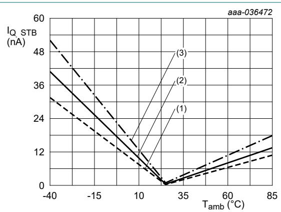
(1): $V_{VBT} = 2.4 V$
$$
V _ {V B T} = 2. 4 \mathrm{V}
$$
$$
V _ {V B T} = 3. 0 \mathrm{V}
$$
$$
V _ {V B T} = 3. 6 \mathrm{V}
$$
(2): $V_{VBT} = 3.0 , V$
(3): $V_{VBT} = 3.6 V$
Fig. 4. I ${Q_STB}$ versus temperature
Fig. 5. I ${Q_CM}$ versus temperature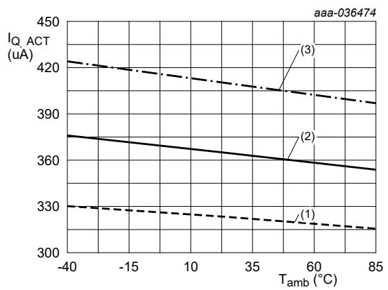
$$
V _ {V B T} = 2. 4 \mathrm{V}
$$
$$
V _ {V B T} = 3. 0 \mathrm{V}
$$
$$
V _ {V B T} = 3. 6 \mathrm{V}
$$
Fig. 6. $I_{Q_ACT}$ versus temperature
Coin cell battery life booster with adaptive power optimization
$\mathbf{V}{\mathrm{VDH}} = \mathbf{V}{\mathrm{SET}} = 2.4\mathrm{V}$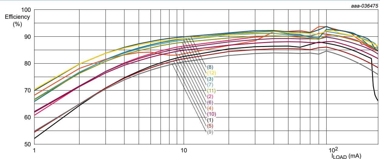
| $V_{VDH} = V_{SET}$ : | $V_{CAP} = 4 V$ | |||
| 1.8 V | 2.4 V | 3.0 V | 3.6 V | |
| -40 °C | (1) | (2) | (3) | (4) |
| 25 °C | (5) | (6) | (7) | (8) |
| 85 °C | (9) | (10) | (11) | (12) |
Fig. 7. Active state efficiency versus load current, VCAP = 4 V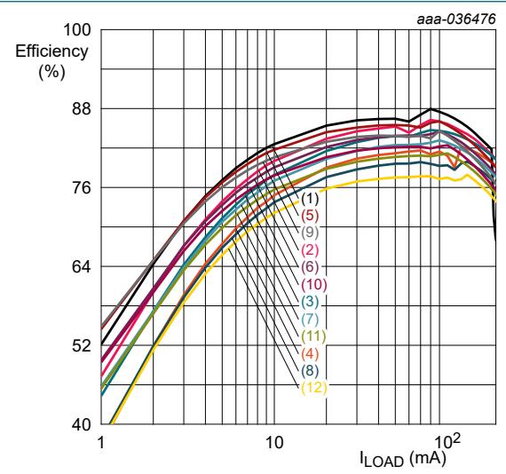
$$
\mathbf {V} _ {\mathrm{VDH}} = \mathbf {V} _ {\mathrm{SET}} = 1. 8 \mathrm{V}
$$
| VCAP: | 4.0 V | 6.0 V | 8.0 V | 11.0 V |
| -40 °C | (1) | (2) | (3) | (4) |
| 25 °C | (5) | (6) | (7) | (8) |
| 85 °C | (9) | (10) | (11) | (12) |
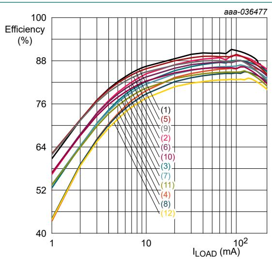
Fig. 8. Active state efficiency versus load current, $V_{VDH} = V_{SET} = 1.8 V$
| VCAP: | 4.0 V | 6.0 V | 8.0 V | 11.0 V |
| -40 °C | (1) | (2) | (3) | (4) |
| 25 °C | (5) | (6) | (7) | (8) |
| 85 °C | (9) | (10) | (11) | (12) |
Fig. 9. Active state efficiency versus load current, $V_{VDH} = V_{SET} = 2.4 V$
Coin cell battery life booster with adaptive power optimization
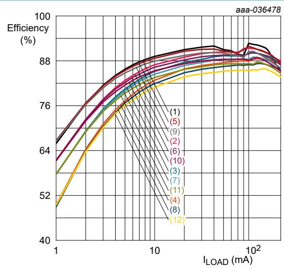
$$
\mathbf {V} _ {\mathrm{VDH}} = \mathbf {V} _ {\mathrm{SET}} = 3. 0 \mathrm{V}
$$
| VCAP: | 4.0 V | 6.0 V | 8.0 V | 11.0 V |
| -40 °C | (1) | (2) | (3) | (4) |
| 25 °C | (5) | (6) | (7) | (8) |
| 85 °C | (9) | (10) | (11) | (12) |
Fig. 10. Active state efficiency versus load current, $V_{VDH} = V_{SET} = 3.0 V$
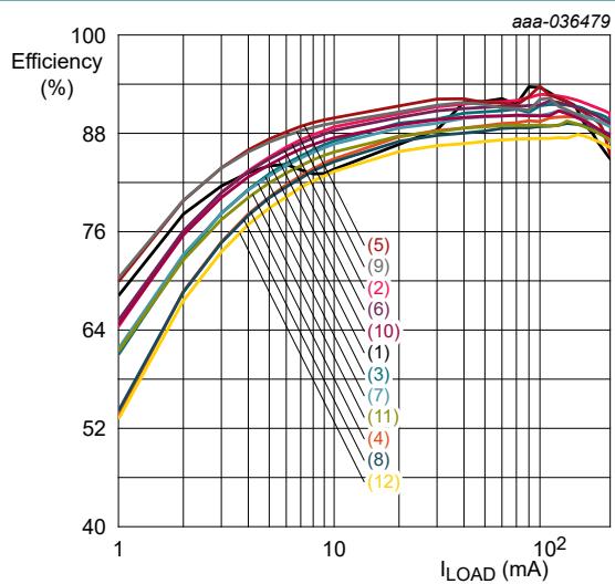
| $V_{VDH} = V_{SET} = 3.6 \text{ V}$ | ||||
| $V_{CAP} :$ | 4.0 V | 6.0 V | 8.0 V | 11.0 V |
| -40 °C | (1) | (2) | (3) | (4) |
| 25 °C | (5) | (6) | (7) | (8) |
| 85 °C | (9) | (10) | (11) | (12) |
Fig. 11. Active state efficiency versus load current, $V_{VDH} = V_{SET} = 3.6 V$
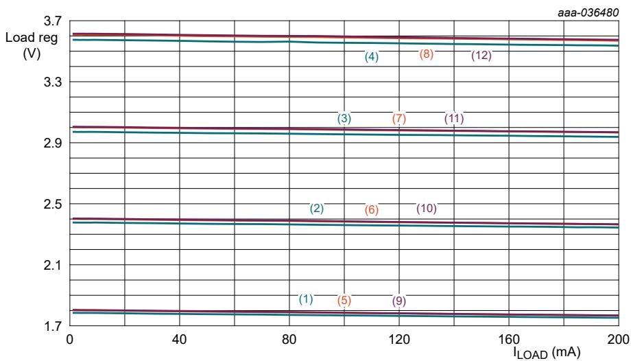
| $V_{VDH} = V_{SET}$ : | $V_{CAP} = 4 V$ | |||
| 1.8 V | 2.4 V | 3.0 V | 3.6 V | |
| -40 °C | (1) | (2) | (3) | (4) |
| 25 °C | (5) | (6) | (7) | (8) |
| 85 °C | (9) | (10) | (11) | (12) |
Fig. 12. Active state $V_{VDH}$ regulation versus load current, $V_{CAP} = 4 V$
Coin cell battery life booster with adaptive power optimization
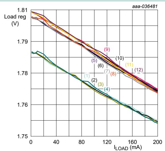
$$
\mathbf {V} _ {\mathrm{VDH}} = \mathbf {V} _ {\mathrm{SET}} = 1. 8 \mathrm{V}
$$
| VCAP: | 4.0 V | 6.0 V | 8.0 V | 11.0 V |
| -40 °C | (1) | (2) | (3) | (4) |
| 25 °C | (5) | (6) | (7) | (8) |
| 85 °C | (9) | (10) | (11) | (12) |
Fig. 13. Active state $V_{VDH}$ regulation versus load current, $V_{VDH} = V_{SET} = 1.8\mathrm{V}$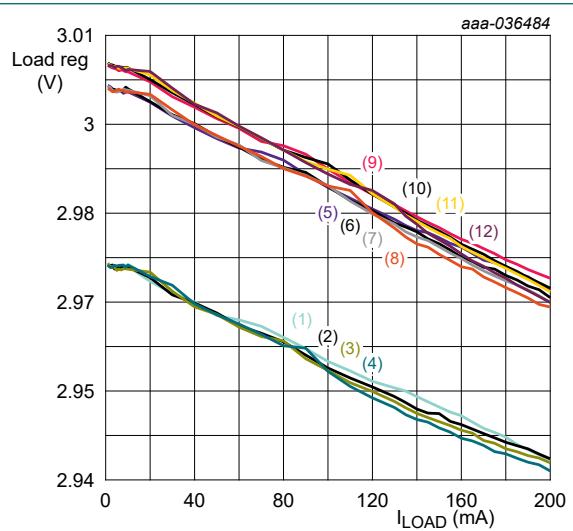
$$
\mathbf {V} _ {\mathrm{VDH}} = \mathbf {V} _ {\mathrm{SET}} = 3. 0 \mathrm{V}
$$
| VCAP: | 4.0 V | 6.0 V | 8.0 V | 11.0 V |
| -40 °C | (1) | (2) | (3) | (4) |
| 25 °C | (5) | (6) | (7) | (8) |
| 85 °C | (9) | (10) | (11) | (12) |
Fig. 15. Active state $V_{VDH}$ regulation versus load current, $V_{VDH} = V_{SET} = 3.0 V$
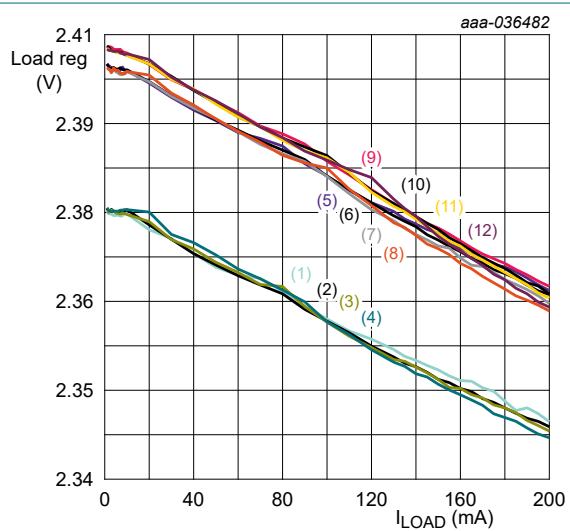
$$
\mathbf {V} _ {\mathrm{VDH}} = \mathbf {V} _ {\mathrm{SET}} = 2. 4 \mathrm{V}
$$
| $V_{CAP}$ : | 4.0 V | 6.0 V | 8.0 V | 11.0 V |
| -40 °C | (1) | (2) | (3) | (4) |
| 25 °C | (5) | (6) | (7) | (8) |
| 85 °C | (9) | (10) | (11) | (12) |
Fig. 14. Active state $V_{VDH}$ regulation versus load current, $V_{VDH} = V_{SET} = 2.4 V$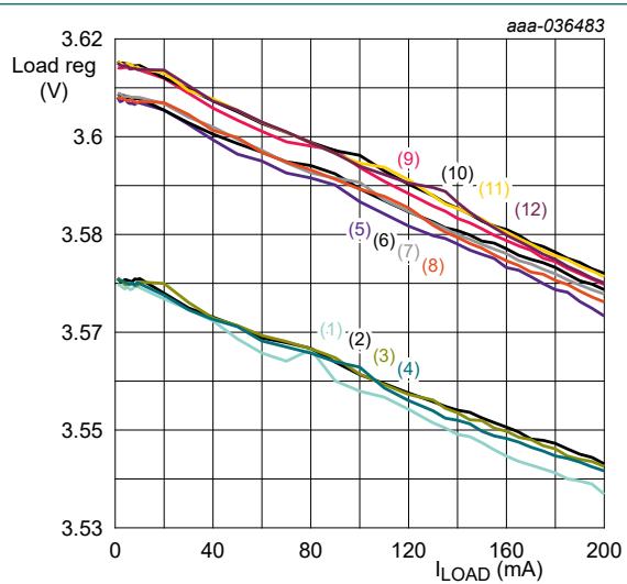
$$
\mathbf {V} _ {\mathrm{VDH}} = \mathbf {V} _ {\mathrm{SET}} = 3. 6 \mathrm{V}
$$
| VCAP: | 4.0 V | 6.0 V | 8.0 V | 11.0 V |
| -40 °C | (1) | (2) | (3) | (4) |
| 25 °C | (5) | (6) | (7) | (8) |
| 85 °C | (9) | (10) | (11) | (12) |
Fig. 16. Active state $V_{VDH}$ regulation versus load current, $V_{VDH} = V_{SET} = 3.6 V$
Coin cell battery life booster with adaptive power optimization
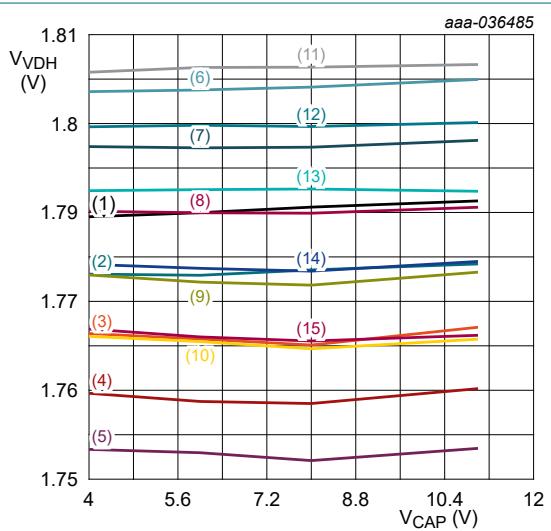
$$
\mathbf {V} _ {\mathrm{VDH}} = \mathbf {V} _ {\mathrm{SET}} = 1. 8 \mathrm{V}
$$
| $I_{VDH}$ : | 10 mA | 50 mA | 100 mA | 150 mA | 200 mA |
| -40 °C | (1) | (2) | (3) | (4) | (5) |
| 25 °C | (6) | (7) | (8) | (9) | (10) |
| 85 °C | (11) | (12) | (13) | (14) | (15) |
Fig. 17. Active state $V_{VDH}$ regulation versus $V_{CAP}$ , $V_{VDH} = V_{SET} = 1.8 V$
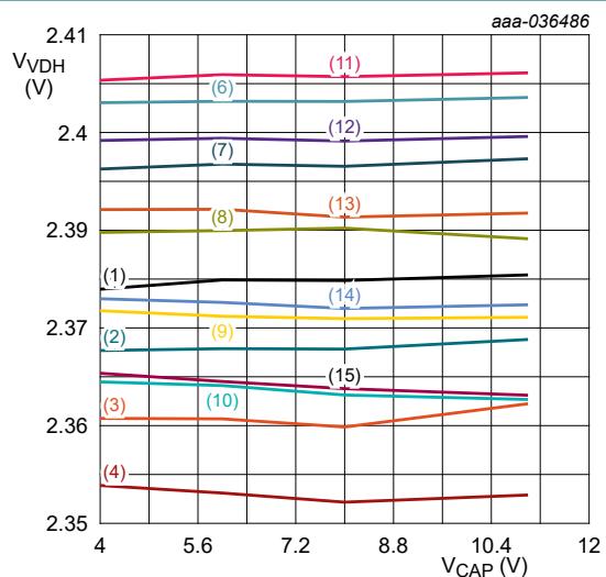
$V_{VDH} = V_{SET} = 2.4 V$
| $I_{VDH}$ : | 10 mA | 50 mA | 100 mA | 150 mA | 200 mA |
| -40 °C | (1) | (2) | (3) | (4) | (5) |
| 25 °C | (6) | (7) | (8) | (9) | (10) |
| 85 °C | (11) | (12) | (13) | (14) | (15) |
$$
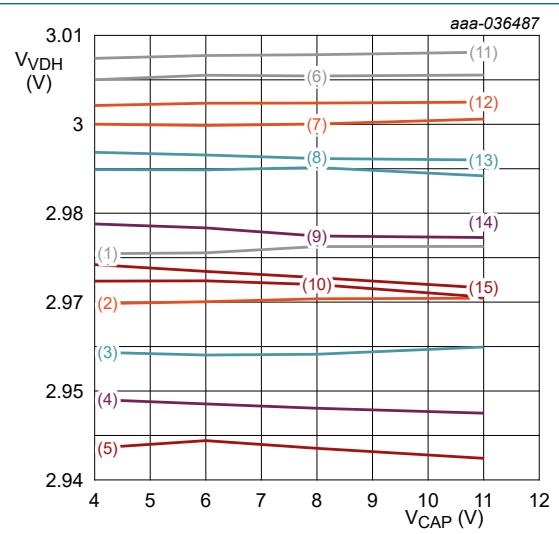
\mathbf {V} _ {\mathrm{VDH}} = \mathbf {V} _ {\mathrm{SET}} = 3. 0 \mathrm{V}
$$
Fig. 18. Active state $V_{VDH}$ regulation versus $V_{CAP}$ , $V_{VDH} = V_{SET} = 2.4 V$
Fig. 19. Active state $V_{VDH}$ regulation versus $V_{CAP}$ , $V_{VDH} = V_{SET} = 3.0 V$
| $I_{VDH}$ : | 10 mA | 50 mA | 100 mA | 150 mA | 200 mA |
| -40 °C | (1) | (2) | (3) | (4) | (5) |
| 25 °C | (6) | (7) | (8) | (9) | (10) |
| 85 °C | (11) | (12) | (13) | (14) | (15) |
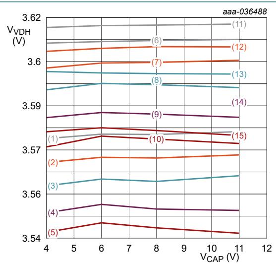
$$
\mathbf {V} _ {\mathrm{VDH}} = \mathbf {V} _ {\mathrm{SET}} = 3. 6 \mathrm{V}
$$
| $I_{VDH}$ : | 10 mA | 50 mA | 100 mA | 150 mA | 200 mA |
| -40 °C | (1) | (2) | (3) | (4) | (5) |
| 25 °C | (6) | (7) | (8) | (9) | (10) |
| 85 °C | (11) | (12) | (13) | (14) | (15) |
Fig. 20. Active state $V_{VDH}$ regulation versus $V_{CAP}$ , $V_{VDH} = V_{SET} = 3.6 V$
Coin cell battery life booster with adaptive power optimization
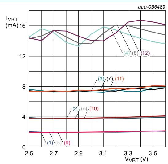
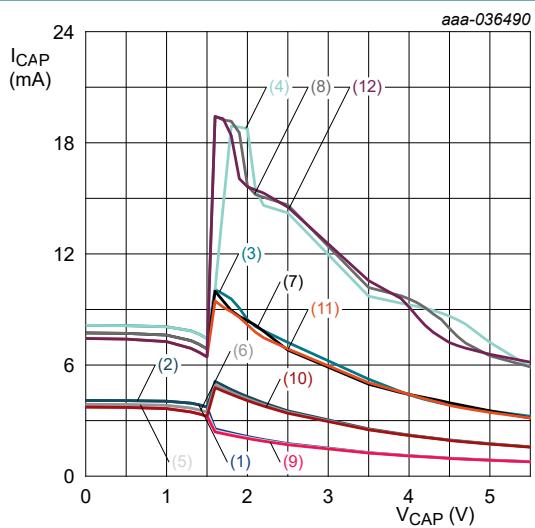
$$
\mathbf {V} _ {\mathrm{CAP}} = 5. 0 \mathrm{V}
$$
| $I_{CH}$ : | 2 mA | 4 mA | 8 mA | 16 mA |
| -40 °C | (1) | (2) | (3) | (4) |
| 25 °C | (5) | (6) | (7) | (8) |
| 85 °C | (9) | (10) | (11) | (12) |
Fig. 21. Charging state supply current $I_{VBT}$ versus supply voltage $V_{VBT}$ , $V_{CAP} = 5.0 V$
$$
\mathbf {V} _ {\mathrm{VBT}} = 3. 0 \mathrm{V}
$$
| $I_{CH}$ : | 2 mA | 4 mA | 8 mA | 16 mA |
| -40 °C | (1) | (2) | (3) | (4) |
| 25 °C | (5) | (6) | (7) | (8) |
| 85 °C | (9) | (10) | (11) | (12) |
Fig. 22. Charging state capacitor current $I_{CAP}$ versus capacitor voltage $V_{CAP}$ , $V_{VBT} = 3.0 , \text{V}$
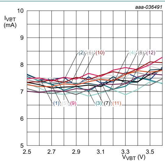
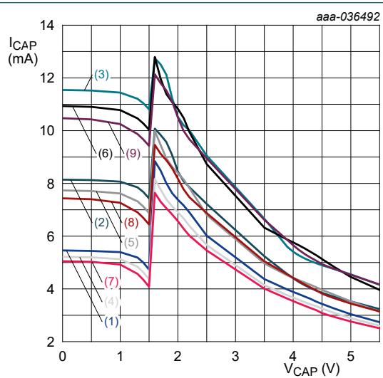
| $I_{CH} = 8 mA$ | $I_{CH} = 8 mA$ | |||||||
| $V_{CAP} :$ | 4.0 V | 6.0 V | 8.0 V | 11.0 V | $V_{VBT} :$ | 2.5 V | 3.0 V | 3.6 V |
| -40 °C | (1) | (2) | (3) | (4) | -40 °C | (1) | (2) | (3) |
| 25 °C | (5) | (6) | (7) | (8) | 25 °C | (4) | (5) | (6) |
| 85 °C | (9) | (10) | (11) | (12) | 85 °C | (7) | (8) | (9) |
Fig. 23. Charging state supply current $I_{VBT}$ versus supply voltage $V_{VBT}$ , $I_{CH} = 8 , mA$
Fig. 24. Charging state capacitor current $I_{CAP}$ versus capacitor voltage $V_{CAP}$ , $I_{CH} = 8 mA$
Coin cell battery life booster with adaptive power optimization
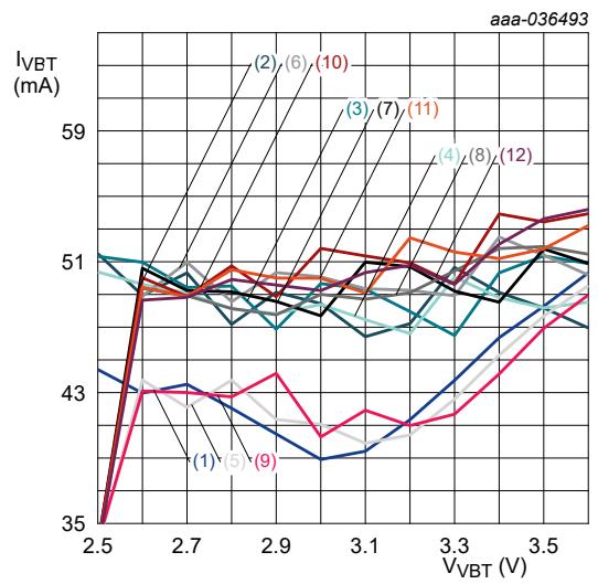
| $I_{CH} = 50 \text{ mA}$ | ||||
| $V_{CAP} :$ | 4.0 V | 6.0 V | 8.0 V | 11.0 V |
| -40 °C | (1) | (2) | (3) | (4) |
| 25 °C | (5) | (6) | (7) | (8) |
| 85 °C | (9) | (10) | (11) | (12) |
Fig. 25. Charging state supply current $I_{VBT}$ versus supply voltage $V_{VBT}$ , $I_{CH} = 50 , mA$
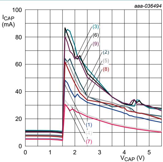
| $I_{Ch} = 50 \text{ mA}$ | |||
| $V_{VBT} :$ | 2.5 V | 3.0 V | 3.6 V |
| -40 °C | (1) | (2) | (3) |
| 25 °C | (4) | (5) | (6) |
| 85 °C | (7) | (8) | (9) |
Fig. 26. Charging state capacitor current $I_{CAP}$ versus capacitor voltage $V_{CAP}$ , $I_{CH} = 50 , mA$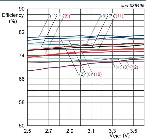
$$
I _ {C h} = 8 \mathrm{mA}
$$
| ${\mathrm{V}}_{\mathrm{{CAP}}} :$ | 4.0 V | 6.0 V | 8.0 V | 11.0 V |
| -40 °C | (1) | (2) | (3) | (4) |
| 25 °C | (5) | (6) | (7) | (8) |
| 85 °C | (9) | (10) | (11) | (12) |
Fig. 27. Charging state efficiency versus supply voltage $V_{VBT}$ , $I_{CH} = 8 , mA$
Coin cell battery life booster with adaptive power optimization
7.9. Timing diagrams
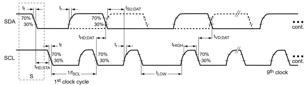
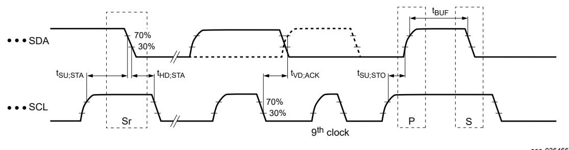
NBM7100A only
Fig. 28. Definition of timing parameters for SCL and SDA signals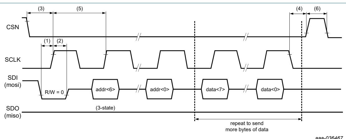
NBM7100B only
Fig. 29. SPI write cycle
Coin cell battery life booster with adaptive power optimization
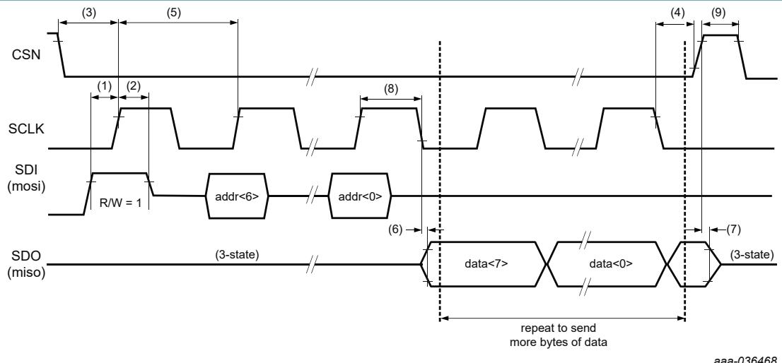
NBM7100B only
Fig. 30. SPI read cycle
Coin cell battery life booster with adaptive power optimization
7.10. Test circuits
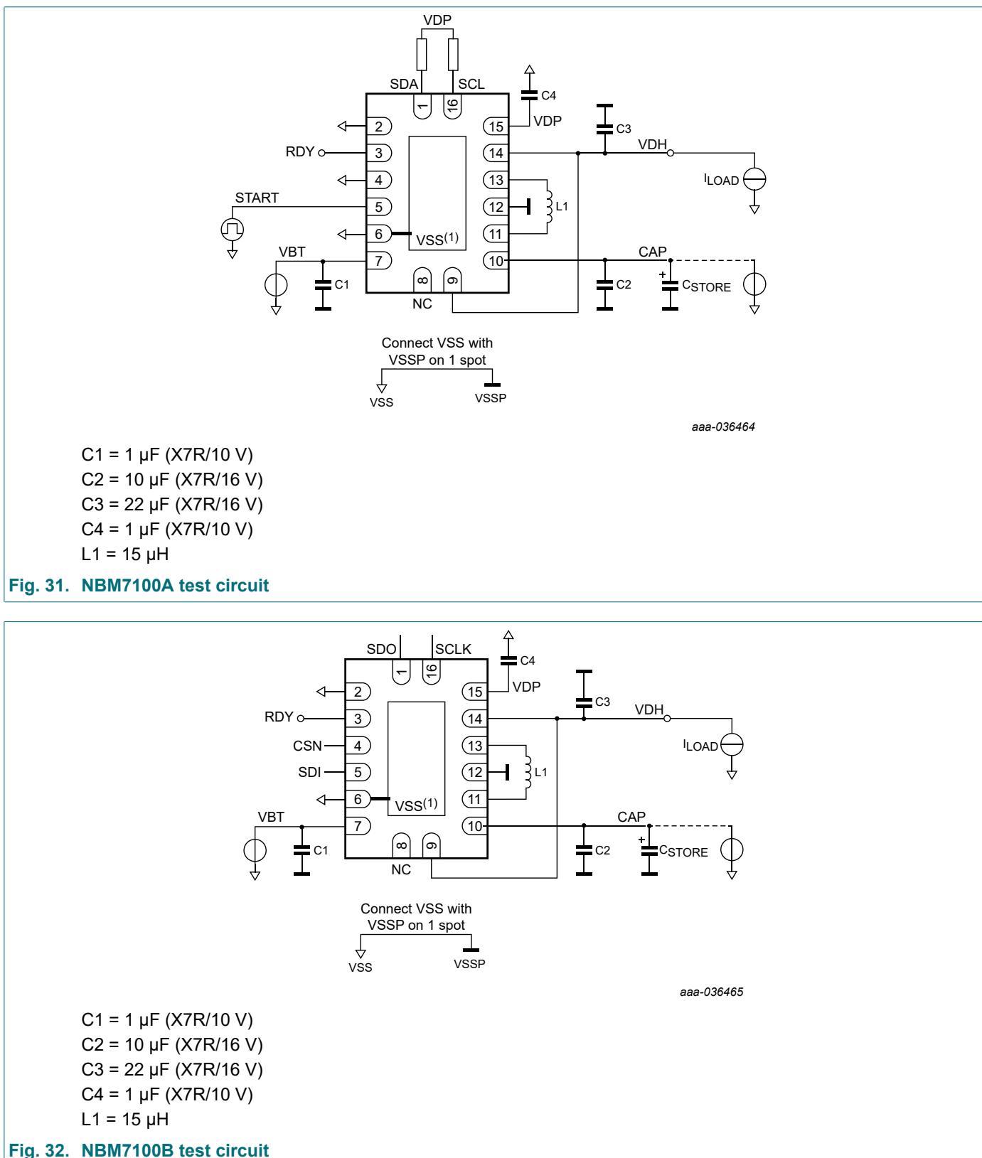
Fig. 32. NBM7100B test circuit
Coin cell battery life booster with adaptive power optimization
8. Detailed description
8.1. Functional diagram
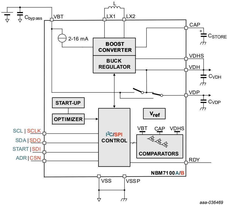
Fig. 33. Functional diagram
8.2. Overview
The NBM7100A/B is a battery energy management device designed to maximize usable capacity from non-rechargeable, primary batteries when used in low-voltage, low-power applications requiring burst current loads.
Battery capacity, expressed as milliampere-hours (mAh) is the amount of current withdrawn from a cell multiplied times the number of hours the cell can deliver the current to a specific end-point voltage, often referred to as the cut-off voltage. Cell capacity varies in response to the applied load and temperature. The shape of the curve depends upon battery construction and chemistry. Primary battery data sheets provide characteristic curves to aid the system designer in estimating the life of the cell under load and temperature conditions. Illustrative, hypothetical characteristic curves are shown in Table 15. Fig. 34 highlights the effect of temperature on primary cell capacity and Fig. 35 shows the result of increasing constant current loading on capacity. The diagrams illustrate how usable battery capacity is adversely affected by both its operating environment and operating condition.
Coin cell battery life booster with adaptive power optimization
Table 15. Example primary battery characteristics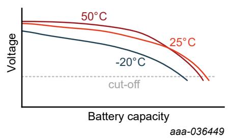
Fig. 34. Battery discharge pattern - constant resistance load at various temperatures
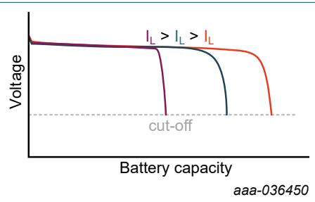
Fig. 35. Battery discharge pattern - constant temperature at various resistance loads
The NBM7100A/B uses two stages of high efficiency DC-DC conversion to buffer the battery from high current, short duration load transients. The first stage conversion, or charge cycle, is initiated in advance of a period of heavy load current. During the charge cycle, energy is transferred from the battery to an external storage capacitor at constant current from the battery. Once charged, the second stage of DC-DC conversion, or active cycle, transfers energy from the storage capacitor to a fixed voltage output capable of supplying high load current. The peak current drawn from the battery remains very low during the charge cycle and is minimal in the active cycle decreasing the repetitive stress on the battery and maximizing the usable capacity. When not operating in charge or active state, the NBM7100A/B enters a low quiescent current standby state. An intelligent learning algorithm monitors the load pulse characteristics and optimizes energy transfer to the capacitor.
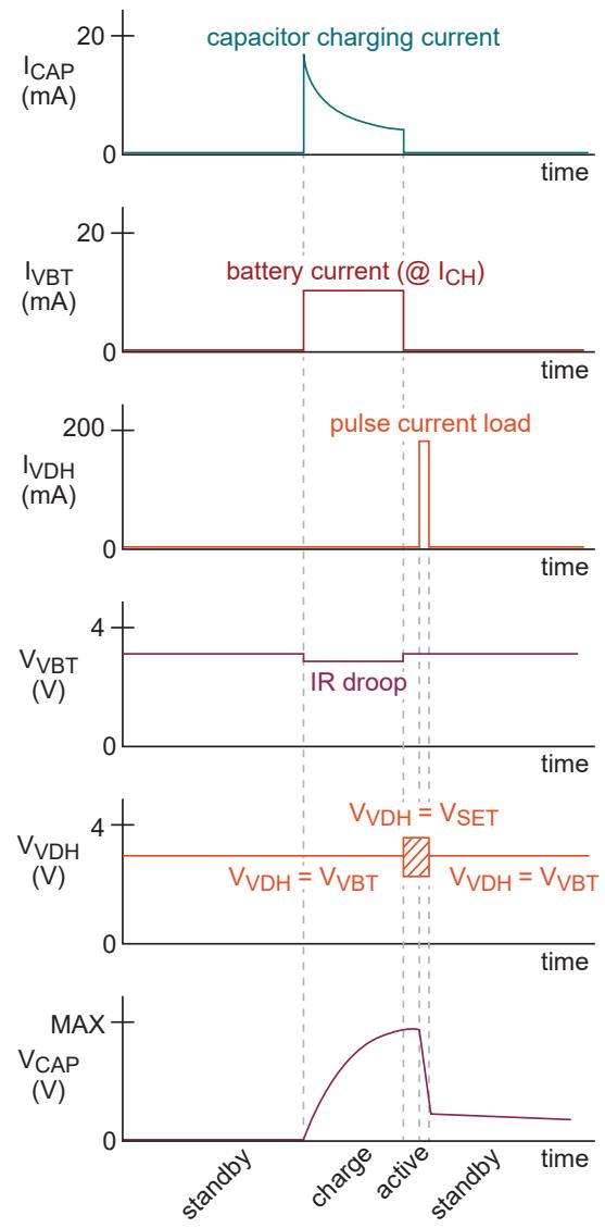
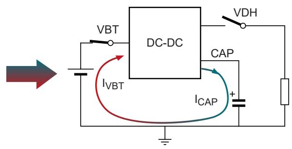
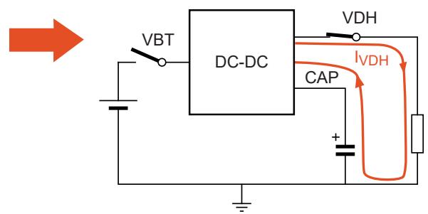
Fig. 36. Standby - Charge - Active - Standby cycle
aaa-036496
Coin cell battery life booster with adaptive power optimization
The NBM7100A/B is ideal for applications supplied from non-rechargeable, primary cell batteries with high internal impedance. Common examples include: lithium metal primary batteries such as 3V lithium manganese dioxide (LiMnO ${2}$ - example "CR 2032 coin cell"), 3.6 V lithium thionyl chloride (Li-SOCl ${2}$ - example "LS 14250" ½ AA), and emerging paper printed types. Lithium metal batteries are commonly selected for low-voltage, low-power electronics due to their superior energy density (Wh/kg) and long storage life. A comparison of lithium batteries is shown in Table 16. The 2 × "AA" alkaline column is included for reference.
Table 16. Basic primary cell battery comparison
| LiMnO2CR 2032 | Li-SOCI2LS 14250 (1/2 AA) | 2 × "AA"Alkaline | |
| open circuit voltage (BoL) | 3 V | 3.6 V | 3 V |
| energy density | 280 Wh/kg | 500 Wh/kg | 200 Wh/kg |
| capacity | 240 mAh (0.2 mA) | 1200 mAh (0.5 mA) | ~ 4000 mAh (@ 250 mA)(2 × 2000mAh) |
| cut-off voltage | 2 V | 2 V | 1.6 V(2 × 0.8 V) |
| shelf life | 10+ years | 10+ years | 5-7 years |
| operating temperature | -30 to 60°C | -55 to 85°C | 0 to 60°C |
| internal resistance [1] | 10 Ω (BoL)70 Ω (EoL) | 10 Ω (BoL)70 Ω (EoL) | < 1 Ω (over lifetime) |
[1] BoL: Beginning of life
EoL: End of life
Many battery powered electronic loads do not operate with a constant current drain from the primary cell, rather are made of short periods of relatively high current followed by much longer periods of very low current. The resulting average current is very low, often only a few 10s of $\mu$ A. It is complicated to accurately estimate the effect variable loading on battery capacity, but important to realize the usable capacity will be lower than the average indicates as the chemical reaction rate needed to support a load pulse of $t_{ON}$ is higher than that required in the $t_{OFF}$ condition scales non-linearly.
Fig. 37 depicts a pulsed load having a peak current $I_{PK}$ and a background (continuous) current drain of $I_{BKG}$ . During the load pulse, the battery voltage droops for two reasons Fig. 38: 1) $I \times R$ drop due to the pulsed current and 2) the chemical reaction rate in response to the load step. When the $I_{PK}$ is released and the battery loading returns to $I_{BKG}$ , the battery voltage returns close to its value before the load pulse was applied. Over time and repetitive pulses, battery chemicals are depleted and the starting and recovery voltages decrease.
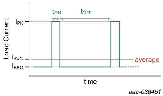
Fig. 37. Pulsed load
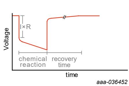
Fig. 38. Battery voltage under pulsed load
Coin cell battery life booster with adaptive power optimization
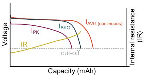
Fig. 39 compares a continuous current drain, $I_{AVG}$ equal to the duty cycle average of $I_{PK}$ and $I_{BKG}$ to the piecewise components of $I_{PK}$ and $I_{BKG}$ to illustrate battery capacity under pulsed conditions are not equivalent to a steady-state current drain of an average equivalent load. Maximum battery life is achieved when the battery is exposed to low DC current, ideally < 10 mA.
aaa-036453
Fig. 39. Battery capacity: pulsed load vs continuous load
Coin cell battery life booster with adaptive power optimization
8.3. Operating modes
The NBM7100 has three operating modes:
Continuous mode
On-demand mode
Auto mode (NBM7100A only)
When the NBM7100A/B is in one of the three operating modes, the device may transition between different States of operation: Standby, Charge, or Active. The Standby state is not an Operating mode, but is represented in Fig. 40 for clarity of device behavior while not in one of the three operating modes.
8.3.1. Mode overview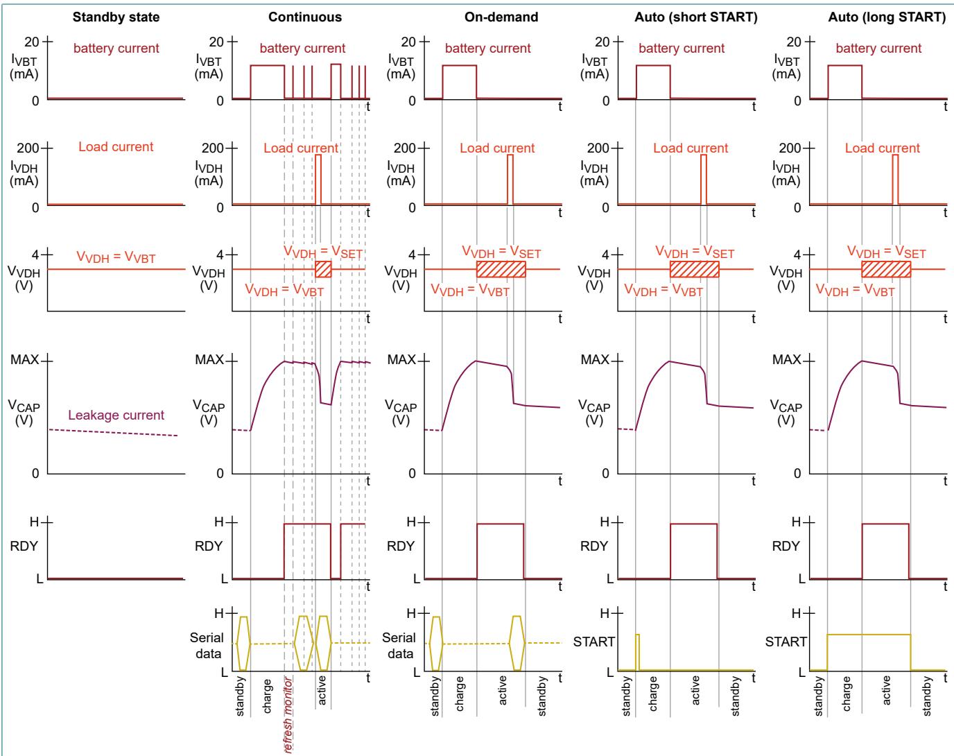
Fig. 40. Mode diagrams
Coin cell battery life booster with adaptive power optimization
Mode Controls
Table 17. command and set3 Registers - Mode control
| Register 80x08(write) | Code (bin) | Function | Remark |
| bit [0] eod(enable On-demand) | 0 | off | - |
| 1 | on | - | |
| bit [1] ecm(enable Continuous mode) | 0 | off | - |
| 1 | on | - | |
| bit [2] act(force Active state) | 0 | off | - |
| 1 | on | force active | |
| bit [3] rstpf(reset optimizer) | 0 | - | - |
| 1 | reset | reset optimizer result of active profile prof[5:0] | |
| Register 11 (write) | |||
| bit [7] automode | 0 | off | default for NBM7100B version [1] |
| 1 | on | default for NBM7100A version | |
[1] NBM7100B cannot be written to 1.
8.3.2. Continuous mode
Continuous mode is intended for applications requiring instant pulse load capability. It is initiated by setting the ECM bit 0x08[1] (see Mode controls). In Continuous mode, the external storage capacitor is charged and the DC-DC converter is idled. The CAP pin voltage is "monitored," and if the capacitor voltage, $V_{CAP}$ as indicated in vcap drops below the end of charge $V_{FIX}$ as programmed in vfix the DC-DC is automatically enabled to "refresh" the capacitor to the target $V_{FIX}$ voltage. When an Active command is received then the stored energy in the capacitor is immediately available at full power as a regulated supply voltage at pin VDH. The storage capacitor will get recharged automatically after the device has delivered its energy pulse to the load. The RDY signal indicates when the storage capacitor has been charged or recharged to $V_{FIX}$ . Active state and recharging can be toggled as needed. The device returns to Standby mode by resetting both the ECM and ACT bits.
8.3.3. On-demand mode
On-demand mode is initiated by setting eod bit 0x08[0] (see Mode controls). This mode is intended to maximize battery lifetime in low duty cycle applications where the system is in sleep-mode most of the time. In this mode the energy is first extracted from the battery and stored in a capacitor ( $C_{store}$ ) connected to the CAP pin. The stored energy is then made available at full power as a regulated supply voltage at pin VDH. The RDY output indicates when the output VDH is ready to deliver power. On-demand mode is ended by resetting the eod and act bits.
8.3.4. Auto mode (NBM7100A only)
Auto mode utilizes the START pin to set and reset the eod bit without requiring the serial bus. One cycle is initiated by a rising edge on the START pin. When charging is finished the Active state will begin automatically and the RDY pin will go high to confirm that the VDH pin is regulating to $V_{SET}$ and ready to deliver full power. The Auto mode can be enabled or disabled by the automode bit 0x0B[7]. To prevent unintended Auto mode triggering due to a floating input condition, the START pin should be connected to VSS via a pull-down resistor. The pull-down resistor should be sized appropriately for the $I_{OH}$ of the external microcontroller driving the pin.
In Auto mode, there are two ways to define the end of the Active state:
- Short pulse on START: From standby mode, a short pulse ( $\geq 10 \mu s$ ) is applied on the START pin. A charge cycle initiates followed by automatic transition to Active state. A short START pulse is defined as the time the START pin is driven high until Active state is reached at the conclusion of the Charge state. $10 \mu s \leq t_{START(short)} \leq time_{(Charge state ends)}$ as indicated
Coin cell battery life booster with adaptive power optimization
by the rdy bit or the RDY pin. The Active state automatically ends when the combined VDP and VDH load current is below $I_{NL}$ for approximately $T_{NL}$ .
- Long pulse on START: From standby mode, the START pin is driven high and maintained high until the Active cycle begins as indicated by a high transition on the RDY pin. The Active state is ended when the START pin is driven low. When a long START pulse is initiated, the START pin should be maintained high until the high current load pulse on VDH is concluded.
Note: in case the START pin is set low during the charge state, this will be interpreted as a short pulse.
At power-on, the default settings of the NBM7100A are:
• Auto mode is ON (see Mode controls)
• $V_{SET} = 3.0 V$
- $I_{\mathrm{ch}} = 8 \mathrm{~mA}$
• Profile number = 1 (Optimization is active for profile 1)
When other settings are required, a serial bus command is required to change the default settings.
The NBM7100A can be switched between Continuous mode, On-demand mode and Auto mode at any time.
8.4. Feature description
8.4.1. Chip control
Refer to functional diagram. The chip control consists of the device state machine; serial bus interface; status, configuration and control registers; the optimizer engine, and fuel gauge functions. It enables and disables peripheral analog blocks as required to execute the state machine.
8.4.1.1. Serial bus
The NBM7100A/B is controlled using a serial bus interface. Reading or writing of settings may be performed approximately 20 ms after power-on reset is cleared and device start-up completed. Initiating communication while the device is in startup may result in register errors. Internal registers allow control of the Standby-Charge-Active cycling process (On-demand mode) or the Charge-Active cycling process (Continuous mode), reading of device status indications, and adjustment of device operating parameters.
8.4.1.1.1. NBM7100A I²C interface
The NBM7100A is protocol compatible to Fast Mode Plus I²C interface (1 MHz). The NBM7100A is a slave device and has two programmable slave addresses. Each I²C transaction requires a register address followed by one or more data bytes. The register address is auto-incremented after each data-byte.
For reading data, the selection of the register address and the reading of the data must occur in one single transaction. Switching from write to read mode (or vice versa) must be done with a repeated Start condition. Register selection is always cleared after a STOP (P) command. If no register is selected while reading, the status register will appear as the first data byte.
| Single byte write to register (N) | |||||||||
| S | SLAVE ADDRESS | W | A | DATA (REG ADDR = N) | A | DATA (N) | A | P | |
| Multiple byte write to register (N + 1) | |||||||||
| S | SLAVE ADDRESS | W | A | DATA (REG ADDR = N) | A | DATA (N) | A | DATA (N + 1) | A P |
| Multiple read from register (M) and (M + 1) | |||||||||
| S | SLAVE ADDRESS | W | A | DATA (REG ADDR = M) | A | Sr | SLAVE ADDRESS | R A | DATA (M) A DATA (M + 1) A P |
| Multiple read of registers (0 - 2) | |||||||||
| S | SLAVE ADDRESS | R | A | DATA (0) | A | DATA (1) | A | DATA (2) | A P |
| LegendFrom Master to Battery Booster S Start condition W Write bit (0) A Acknowledge bitFrom Battery Booster to Master P Stop condition R Read bit (1) Sr Repeated Start condition | |||||||||
Fig. 41. I²C transfers
Coin cell battery life booster with adaptive power optimization
Two I²C slave addresses are available for the NBM7100A :
Table 18. I²C addresses
| ADR pin | I2C Slave address |
| 0 | 0x2E (010 1110 R/Wn) |
| 1 | 0x2F (010 1111 R/Wn) |
8.4.1.1.2. NBM7100B Serial Peripheral Interface (SPI)
The NBM7100B supports bidirectional communication with a master system controller (MCU) via a 4-wire SPI mode 0 compatible serial communication interface. It is a transmit/receive slave-only interface. The master device initiates data transfers on the bus and must generate the Clock (SCLK) and Chip Select Not (CSN) signals. The data input is SDI (MOSI), and the data output is SDO (MISO). Each transmission starts with the falling edge of CSN and ends with the rising edge. During a transmission, commands and data are controlled by SCLK and CSN according to the following rules:
- Commands and data are shifted MSB first, LSB last.
• Input bit is sampled at the rising edge of SCLK.
- In read mode, data bits are shifted out at the falling edge of SCLK. After the device has been selected with the falling edge of CSN, the first byte defines data direction and register address. MSB = 1 for Read, or MSB = 0 for Write, followed by 7-bits for the address in the register space.
- The rising edge of CSN ends all data transfer, terminating any previous command and clears the address pointers.
- If an invalid command is received, no data is shifted out of the circuit until the falling edge of CSN. This reinitializes the serial communication.
• Data that is written to the NBM7100B immediately follows the first address byte.
• Data that is read from the device at the rising edge of SCLK immediately follows the last bit of the address byte.
• Maximum SCLK clock frequency is 4 MHz (500 Kbyte/s)
- An SPI command can be followed by multiple data bytes within one transmission. The register address pointer is auto-incremented.
- SPI mode 0 means that the parameters Clock Polarity (CPOL) and the Clock Phase (CPHA) are both 0.
8.4.1.1.3. Device register overview
Refer to the register map. Short description of the registers and their functions follows. Additional details can be found in the respective feature sections.
setx registers [0x09:0x0D] configure the active mode regulated output voltage vset[3:0] ( $V_{DH}$ ); the charge state target voltage vfix[3:0], $V_{FIX}$ and maximum voltage for the storage capacitor vcapmax ( $V_{CAP(MAX)}$ ); the capacitor charging current ich[2:0] ( $I_{CH}$ ); low voltage monitor thresholds for battery vmin[2:0] ( $V_{MIN}$ ), and capacitor early warning vew[3:0] ( $V_{EW}$ ); enable/disable the internal power path switch between $V_{DP}$ and $V_{DH}$ vdhhiz; enable/disable auto mode automode; and adjust the voltage margin of the optimizer function opt_marg[1:0].
status register [0x00] provides indication the capacitor is charged and is the device is ready (rdy) to support a high current load on the $V_{DH}$ pin. The RDY output pin reflects the present status of the rdy bit without requiring serial bus data transactions. Monitor alarms for low battery, $V_{MIN}$ , (lowbat); low capacitor voltage, $V_{EW}$ , early warning (ew) and low output voltage in the Active state, $V_{DH}$ (alarm) provide a view of device and system conditions.
command register [0x08] is used to set the device operating modes: enable On-demand, enable Continuous, and Active. The MSBs of [0x08] and LSBs of [0x07] are used to set the optimizer profile number prof[5:0] (1d to 63d). Each profile setting can be used optimize the energy transfer of one unique repetitive load condition (see Section 8.4.5). The least significant bits of the optimizer profile setting are deliberately located in the command register to facilitate a single write transaction for the first 14 settings (1d to 14d).
vcap register [0x05] is utilized in the charge and active states to provide near real-time indication of storage capacitor voltage. The registers are not updated in the standby state. The vchend register is a translated digital mapping of the target $V_{CAP}$ voltage obtained from vfix[3:0] in [0x08] when the prof[5:0] bits are all reset [0h], or voptx[3:0] hidden registers used by the optimizer to set the target capacitor charging voltage threshold associated with each profile.
chengy registers [0x01:0x04] provide indication of the charge removed from the battery following one enable On-demand or upon completion of a Continuous mode cycle. The registers are reset before the charging cycle begins and should be read and accumulated by an external microcontroller while the device is in the active or standby state.
Coin cell battery life booster with adaptive power optimization
8.4.1.2. The ready (RDY) output signal and rdy bit
The RDY signal is driven high indicating that the NBM7100A/B is ready to provide full power to its load. It can serve as an interrupt signal to a connected microcontroller. Its behavior is different (see below) in On-demand mode than it is in Continuous mode. The rdy bit in 0x00[0] follows the RDY signal.
RDY in On-demand mode
The RDY signal will go high when the capacitor charge level is reached, and the VDH output voltage is regulating to $V_{SET}$ .
The RDY signal will go low if:
• The eod bit is reset (see Mode controls) or
• The storage capacitor is depleted.
If Early Warning is activated and the voltage at the storage capacitor drops below $V_{EW}$ (see capacitor early warning voltage), then the RDY signal will pulse low for $t_{EW}$ , then resume high state until one of the above On-demand mode conditions is met.
RDY in Continuous mode
The RDY signal will go high when the voltage at pin CAP has reached $V_{FIX}$ .
The RDY signal will go low if:
• The act bit is reset (see Mode controls) or
• The storage capacitor is depleted.
If Early Warning is activated and the voltage at the storage capacitor drops below $V_{EW}$ (see capacitor early warning voltage), then the RDY signal will pulse low for $t_{EW}$ , then resume high state until one of the above Continuous mode conditions is met..
8.4.2. States of operation
The NBM7100A/B has four main states of operation as shown in Table 19.
Table 19. States of operation
| <img src="images/f28ab985c229496993d629f192938bec8db1719136e87d0e72468c7828c362d7.jpg"/> | Continuous mode | On-demand mode | Auto mode | |||
| (1) ecm bit set | 010 | (1) eod bit set | 001 | (1) 10 μs start pulse | 001 | |
| (2) act bit set | 110 | (2) Charge ready | 101 | (2) Charge ready | 101 | |
| (3) act bit reset | 010 | (occurs autonomously) | (4) no_load current | 000 | ||
| ......from Charge or Active return to Standby: (4) Reset ecm and act | 000 | (4) eod bit reset | 000 | |||
| (1) eod bit set | 001 | (1) START = 1 | 001 | |||
| (2) Force active | 101 | (2) Charge ready | 101 | |||
| (before Charge ready) | (4) START = 0 | 000 | ||||
| (3) Continue charge | 001 | |||||
| (2) Charge ready | 101 | |||||
| (occurs autonomously) | ||||||
| (4) EOD bit reset | 000 | |||||
| The three digits represent the value of the bits (act; ecm; eod) in register 8 (see Section 10.2), either controlled through a serial bus command, or (in bold italic) changed by the internal logic. | ||||||
8.4.2.1. Startup state
When a battery or other voltage source is sensed at the VBT pin and the sensed voltage is higher than $V_{POR}$ level, internal power switches connect VBT and outputs VDP and VDH (See POR VBT fast ramp). Approximately 20 ms after start-up, the Standby state is entered.
Coin cell battery life booster with adaptive power optimization
Note: The register map indicates the default state of all bits at startup. Reading or writing to the serial bus during the Startup state may cause corruption of the non-volatile memory. Serial bus transactions should not be initiated until approximately 20 ms after $V_{VBT} > V_{POR}$ when the device has entered the Standby state.
8.4.2.2. Standby state
The Standby state is a low power operating condition where the quiescent current consumption is almost negligible; the serial port is active and ready to receive commands; and the VBT to VDP switch is enabled.
In the Standby state, the device is inactive. The supply current drawn from the battery is very low, $I_{Q_STB}$ and the device is waiting for a serial bus command or START command (NBM7100A). While the device is in Standby state, device settings can be programmed. For example: maximum storage voltage, $V_{CAP(MAX)}$ ; the charging current, $I_{CH}$ ; and the active mode VDH output voltage, $V_{SET}$ .
The VBT to VDH switch is enabled at POR by default. Alternatively, for a high-impedance VDH output in the Standby and Charge states, set vddhhiz = 1 (see VDH).
The register settings are retained while supply voltage at VBT input is not interrupted.
The RDY output and rdy register bit is low in Standby state.
The chip will exit Standby and enter the Charge state by:
• the setting of eod (Enable On-demand) bit, or
- setting the ecm (Enable Continuous Mode) bit, or
• activation with the START pin (NBM7100A) with automode = 1.
8.4.2.3. Charge state
The DC-DC boost converter is enabled with VBT as the input and CAP as the output. The external storage capacitor is charged from VBT using constant current, $I_{CH}$ , as set by the ich[3:0] bits in 0x0A[7:5]. The ich bits provide 4 normal charging current settings and one high current (emergency) level. Using the lowest $I_{CH}$ setting maximizes battery life at the expense of a long charging time.
In the Charge state, if $V_{VBT}$ drops below the programmed VBT input minimum threshold, $V_{MIN}$ as set by the vmin[2:0] bits in 0x0A[2:0], the NBM7100A/B pauses charging until VBT recovers above $V_{MIN}$ at which point charging resumes. If VBT remains below the $V_{MIN}$ threshold for more than 16 $\mu$ s, the lowbat alarm status bit will be set to indicate the battery may be nearing end of life.
vmin[2:0] is an aid for maintaining a minimum battery voltage. Battery voltage drop could be caused by multiple factors including, current consumed by other functions in the application connected directly to the battery, end of battery life, a low operating temperature or the formation of a passivation layer inside the battery (in case of Li-Thionyl batteries).
While above $V_{MIN}$ , charging continues until the “End-of-charge” voltage is reached.
- Fixed (optimizer disabled): The "End-of-charge" voltage as set by vfix (optimizer profile = 0)
- Optimizer (enabled): The “End-of-charge” voltage as set by voptx (hidden register location) as controlled by the optimizer (optimizer profile ≠ 0)
The vcapmax bit in 0x0C[4] defines, $V_{\mathrm{CAP(MAX)}}$ , the maximum storage capacitor voltage allowed during the Charge state. For safety reasons the value $V_{\mathrm{CAP(MAX)}}$ will never be exceeded even if a higher fixed End-of-charge voltage is programmed.
The progress of charging the storage capacitor can be monitored by reading the vcap status register 0x05[4:0].
In On-demand mode, the device will automatically enter Active state after reaching the End-of-charge voltage.
In Continuous mode the device will stay in Charge state and the charge level of the capacitor will be maintained at the programmed level. This will compensate for any leakage from the storage capacitor. This charge maintenance uses minimal power from the battery.
8.4.2.4. Emergency charge state
The normal charge currents ich[3:0] = 0h, 1h, 2h, or 3h are intended to limit the battery current for optimal efficiency and battery lifetime. The lower the charge current, the longer the time to charge the storage capacitor. In cases where a shorter charge time prevails above battery lifetime, the emergency charge mode (ich[3:0] = 4h) is available. In emergency charge mode, the battery current is increased to 50 mA (typical). vmin[2:0] continues to function as described in Charge state.
Coin cell battery life booster with adaptive power optimization
8.4.2.5. Active state
In the Active state both the VDP and VDH outputs are supplied from the integrated switching regulator using the storage capacitor as its energy source. In this state the current consumed by the NBM7100A/B from the battery is very low, $I_{Q_ACT}$ . The output voltage (VDP and VDH) is determined by the value programmed in the set1 register using the vset[3:0] ( $V_{SET}$ ) bits.
On-demand mode: The Active state is entered automatically after charging has been completed. The Active state can also be initiated prior to completion of the charge cycle (force active) by setting the act bit high. Active state ends by resetting the eod bit and returns to the Standby state.
Continuous mode: The Active state is entered at any time by setting the act bit. Active state ends by resetting the act bit and returns to the Charge state. Resetting the ecm and act bits returns the device to Standby.
8.4.2.6. Capacitor input voltage Early Warning alarm
In the Active state the storage capacitor is the energy source for the DC-DC converter. As the capacitor is discharged by the load its voltage drops. A programmable early warning alarm is available to alert the system when $V_{CAP}$ drops below the $V_{EW}$ threshold set by the vew[3:0] bits indicating a limited amount of energy is remains in the capacitor. The eew bit enables or disables the alarm indication. The condition of the alarm is indicated by the ew bit in the status register 0x00[6]. When the ew bit goes high, the RDY pin pulses low for $t_{EW}$ providing two mechanisms for the system to receive an indication the alarm has triggered. The power on default state for eew is disabled.
8.4.2.7. VDH output voltage alarm
In the Active state, if the load current exceeds the capability of the regulator, the VDH voltage may drop below the programmed target voltage, $V_{SET}$ triggering the VDH alarm. The condition of the alarm is indicated by the alarm bit in the status register 0x00[5]. When the alarm bit is set, the RDY pin is driven low providing dual mechanisms for the system to receive the indication. If the load current is reduced, VDH may recover to $V_{SET}$ before the Active state concludes; however, the alarm bit and RDY pin low indications will not reset until the next Charge state is initiated.
The maximum load current depends on the operating point of the DC-DC converter in the Active state: capacitor voltage (input supply to the DC-DC); the programmed VDH voltage $V_{SET}$ (output of the DC-DC); external components ratings and tolerances; and the ambient temperature. Some typical characteristics are given in Application curves.
Coin cell battery life booster with adaptive power optimization
8.4.3. DC-DC converter
The NBM7100 integrates a variation of a classical peak-current mode control "4-switch buck-boost" with a fixed frequency of 1 MHz. The DC/DC converter operates with discontinuous conduction mode for light loads and transitions to continuous conduction mode as the load current increases. Refer to Fig. 42.
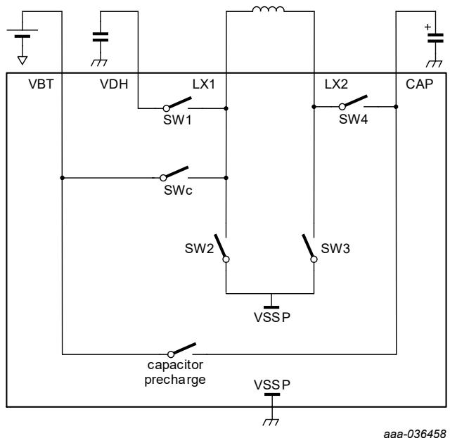
Fig. 42. DC-DC converter switches
In the charge state when $V_{CAP} < 1.6$ V, the storage capacitor is initially charged at low current via the capacitor precharge switch.
In the Charge state when $V_{CAP} > 1.6$ V, the DC-DC converter operates in boost mode to draw constant programmed charging current ( $I_{CH}$ ) from the battery and charge the energy storage capacitor connect to the CAP pin.
The charging transition threshold can be seen in the typical characteristics section of the datasheet in the charging state capacitor current $I_{CAP}$ versus capacitor voltage, $V_{CAP}$ plots.
Boost mode (Charge)
• Primary phase: SWc and SW3 are ON
• Secondary phase: SW2 and SW4 are ON
In the Active state, the dc/dc converter uses the energy available in the storage capacitor to deliver a regulated output ( $V_{SET}$ ) on the $V_{DH}$ pin capable of supporting pulsed current loads.
Buck mode (Active)
• Primary phase: SW1 and SW4 are ON
• Secondary phase: SW1 and SW3 are ON
Coin cell battery life booster with adaptive power optimization
8.4.4. VDP and VDH output configuration
Fig. 43 provides a simplified representation of the internal power switches within the NBM7100A/B devices.
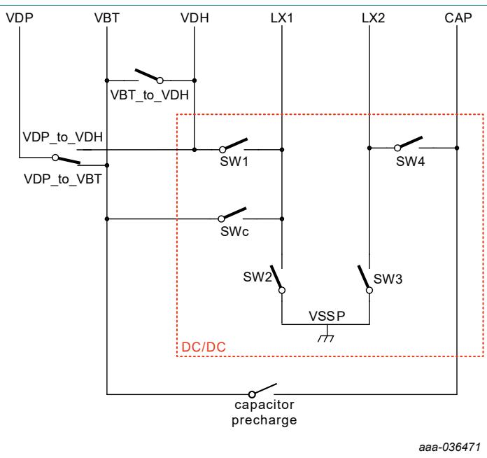
Fig. 43. Internal switches
8.4.4.1. VDP
VDP is a 'permanent' supply output pin. It is internally connected to VBT in the Standby and Charge states via the VDP_to_VBT switch. In the active state, VDP connects to VDH via the VDP_to_VDH switch. It provides power to 'always on' system loads (e.g. host microcontroller core and I/O). Due to the variable range of output voltages between VBT and the regulated VDH, care should be taken to ensure loads connected to the VDP pin will not be subjected unintended over-voltage or under-voltage conditions.
The VDP pin should be connected to a bypass capacitor. See Recommended components.
Coin cell battery life booster with adaptive power optimization
8.4.4.2. VDH
The vdhhiz bit 0x0A[4] is 0b upon entry into the Standby state following POR, connecting VBT to VDH. Unless the vdhhiz is set via the serial interface, VDH pin remains internally connected to VBT in all states of operation except the Active state.
In the Active state, VDH supplies a regulated output voltage according to vset[3:0] in 0x09[3:0]. Table 20 summarizes the device default switch connections.
Table 20. VDP and VDH operation, vdhhiz 0x0A[4] = 0 (default operation)
| State | VDP | VDH | Diagram |
| Standby | Connect to VBT | Connect to VBT | <img src="images/b698bc2f177c172d8d336ce52ef27b41e71659168208113953a004cc9d8c78d0.jpg"/>Fig. 44. Standby and charge |
| Charge | Connect to VBT | Connect to VBT | |
| Active | Connect to VDH | Connect to DC-DC output vset | [IMAGE]Fig. 45. Active |
If the vdhhiz bit 0x0A[4] is set via the serial interface, the VDH output becomes high impedance if the device is not in the Active state as indicated in Table 21. The high impedance configuration is useful in cases where it is preferable to switch off a load (e.g. a sensor) connected to the VDH pin. When the high impedance vdhhiz mode is not required, all loads can be supplied from the VDH pin simplifying system configuration. When high impedance mode is enabled, the host microcontroller should be supplied from the VDP pin or directly from the battery.
Table 21. VDP and VDH operation, vdhhiz 0x0A[4] = 1 (high-Z operation)
| State | VDP | VDH | Diagram |
| Standby | Connect to VBT | Hi-Z | <img src="images/12443ec88de4bd5281aa86cf3701123076e4bf015a2e358dd4c7415440db2a14.jpg"/>Fig. 46. Standby and charge |
| Charge | Connect to VBT | Hi-Z | |
| Active | Connect to VDH | Connect to DC-DC output vset | Fig. 47. Active |
In more complex RF microcontroller applications with multiple input voltage pins, the VDP output can be connected to the core and I/O functions supply inputs, while the VDH output is connected to the high current RF power supply input.
Coin cell battery life booster with adaptive power optimization
The VDH pin should be connected to a bypass capacitor after accounting for derating characteristics to achieve the minimum capacitance indicated in the Recommended components table.
8.4.4.3. Setting VDH output voltage, $V_{SET}$ (Active state)
Upon completion of a Charge state, the device transitions to the Active state at which time VDH becomes a regulated voltage output denoted as $V_{SET}$ as configured in vset[3:0] in 0x09[3:0]. Unless overwritten via the serial bus, the default $V_{SET}$ voltage is 3.0 V.
For some applications it may be beneficial to change $V_{SET}$ during the Active state. For example, an RF microcontroller in a sensor application needs to transmit several data packets to a remote receiver. The initial data packet is transmitted at maximum power likely requiring a $V_{SET}$ voltage of 3.6 V. After receiving an acknowledgement of a successful link with receiver, the RF microcontroller may determine a lower transmit power is sufficient and decrease the $V_{SET}$ voltage dynamically to 3 V for duration of this transmit/receive period.
8.4.5. Adaptive power optimization
The NBM7100A/B applies a proprietary learning algorithm to adaptively determine and optimize the amount of energy to be transferred from the battery and stored in the capacitor. This optimization engine can learn up to 63 load profiles. Each learned profile is retained in a reserved register location used by the optimization engine.
Each optimizer setting is used to store one load profile. Each stored load profile should be reasonably consistent and repetitive in energy requirements.
If prof[5:0] = 0h, the optimizer is disabled and the storage capacitor is charged according to the vfix[3:0] registers.
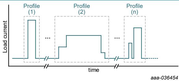
Fig. 48. Load profiles
The optimizer engine works by measuring the residual energy level in the storage capacitor after each load pulse and predicts the optimized energy level to charge the storage capacitor for the next pulse.
Optimizer profile 1 and 'extra safe' optimization margin are enabled by default after the device POR threshold is cleared. Assigning a different profile, prof[5:0] in 0x07, 0x08, or altering the optimization margin, opt_margin in 0x0D, is performed via the serial bus.
The optimizer margin voltages in opt_marg[1:0] correspond approximately to the first four $V_{OPTx}$ levels and is analogous to the first four $V_{FIX}$ levels.
8.4.5.1. Optimizer initialization and downward increment
Each optimizer profile setting learns the repetitive energy requirement of the assigned load. The number of repeated load pulses needed to reach an optimized level will vary depending upon the energy consumed. Reserved register locations maintain the target capacitor charging voltages for each profile, $V_{OPTx}$ . $V_{OPTx}$ is analogous to the user programmable $V_{FIX}$ setting (optimizer profile = 0), the exception being the optimizer engine automatically increments $V_{OPTx}$ during the initial learning phase and in response to changes in the load profile.
At the start of the optimization process, $V_{OPTx}$ is set to $V_{CAP(MAX)}$ according to the vcapmax setting. When On-demand is initiated via register write or START pin (NBM7100A), the capacitor charges to $V_{CAP(MAX)}$ . When charging is complete, the NBM7100A/B initiates an ACTIVE cycle during which the load is applied. At the conclusion of the Active cycle the capacitor voltage is compared to the $V_{OPT_MARGIN}$ , opt_marg[1:0], threshold.
- If $V_{CAP} > V_{OPT_MARGIN}$ , the voptx register is decremented one setting.
- If $V_{CAP} < V_{OPT_MARGIN}$ , the voptx register is incremented by at least one setting.
Fig. 49 is an example of an optimizer initialization sequence. The initialization sequence occurs after device power on, or if the optimizer profile is reset, by selecting a profile number using and writing 1b to rstpf 0x08[3].
Coin cell battery life booster with adaptive power optimization
Initial conditions for initialization example:
Device powered and POR cleared (battery insertion).
vcapmax 0x0C[4] = 1b.
$V_{CAP}$ at zero or holding residual charge.
$V_{OPT_MARGIN}$ 0x0D[1:0] = 11b (default)
prof = 1b (default)
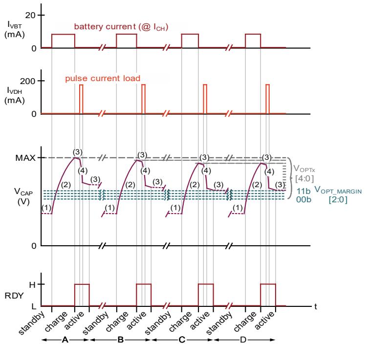
(1) Standby state: $V_{CAP}$ decreases due to leakage current.
(2) Charge: capacitor charged to $V_{OPTx}$ reserved register setting.
(3) Active: DC-DC providing regulated $V_{DH}$ . No load is applied.
(4) Load: load pulse supplied from $V_{DH}$ output.
Fig. 49. Optimizer profile initialization and down increment
Table 22. Optimizer profile initialization and down increment
| A | B | C | D |
| $V_{OPTx} = V_{CAP(MAX)}$ [15d] | $V_{OPTx} = [14d]$ | $V_{OPTx} = [13d]$ | $V_{OPTx} = [13d]$ |
| (1) Standby. | |||
| (2) On-demand cycle initiated: Charging. | |||
| (3) Active, no load. | |||
| (4) Active, with load. | |||
| (3) Active, no load. | |||
| (1) Standby, no load. | |||
| $V_{CAP} > V_{OPT\_MARGIN}$ decrement $V_{OPTx}$ | $V_{CAP} > V_{OPT\_MARGIN}$ decrement $\overline{V}_{OPTx}$ | $V_{CAP} = V_{OPT\_MARGIN}$ no change $V_{OPTx}$ | $V_{CAP} = V_{OPT\_MARGIN}$ no change $\overline{V}_{OPTx}$ |
During A, B, and C as the optimization level is being approached, the charging energy from the battery is reduced becoming approximately constant in D and subsequent repetitions of D (not shown).
If after optimization, the load pulse energy is reduced by either or both reducing the peak current in the pulse, or the time the pulse persists, the state machine takes action to reduce $V_{OPTx}$ until a new optimized level is reached.
Coin cell battery life booster with adaptive power optimization
8.4.5.2. Optimizer upward increment
If after completing an initial or downward optimization sequence as shown in Optimizer initialization and downward increment, the load increases either or both in amplitude or duration, the optimizer state machine will respond with upward incrementation until a new steady-state optimization level is reached.
Initial conditions for upward increment example:
Device has previously optimized the selected load profile.
$V_{CAP}$ at zero or holding residual charge.
$V_{OPT_MARGIN}$ 0x0D[1:0] = 11b (default)
prof = 1b (default)
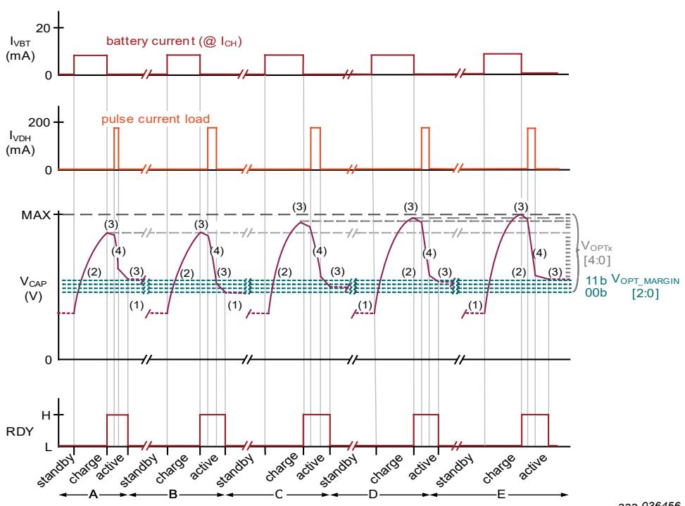
(1) Standby state: $V_{CAP}$ decreases due to leakage current.
(2) Charge: capacitor charged to $V_{OPTx}$ reserved register setting.
(3) Active: DC-DC providing regulated $V_{DH}$ . No load is not applied.
(4) Load: load pulse supplied from $V_{DH}$ output.
Fig. 50. Optimizer up increment
Table 23. Optimizer up increment
| A | B | C | D | E |
| $V_{OPTx} = V_{CAP(MAX)}$ [11d] | $V_{OPTx} = V_{CAP(MAX)}$ [11d]; loadduration increases | $V_{OPTx} = [13d]$ | $V_{OPTx} = [14d]$ | $V_{OPTx} = [15d]$ |
| (1) Standby. | ||||
| (2) On-demand cycle initiated: Charging. | ||||
| (3) Active, no load. | ||||
| (4) Active, with load. | ||||
| (3) Active, no load. | ||||
| (1) Standby, no load. | ||||
| $V_{CAP} = V_{OPT\_MARGIN}$ no change $V_{OPTx}$ | $V_{CAP} < V_{OPT\_MARGIN}$ increment $V_{OPTx}$ | $V_{CAP} < V_{OPT\_MARGIN}$ increment $V_{OPTx}$ | $V_{CAP} < V_{OPT\_MARGIN}$ increment $V_{OPTx}$ | $V_{CAP} = V_{OPT\_MARGIN}$ no change $V_{OPTx}$ |
Coin cell battery life booster with adaptive power optimization
During B, the change in load is large enough to result in an ending $V_{CAP}$ voltage well below optimizer margin voltage (11b) and results in an incrementation of two steps. At the conclusion of C and D, $V_{CAP}$ is remains below the optimizer margin voltage, but is less severe resulting in a single step increments. The energy transferred from the battery increases in each cycle. In E, the $V_{CAP}$ is just above the margin voltage and optimization is complete. Subsequent load profiles identical to E will not change the $V_{OPTx}$ and are not shown.
8.4.5.3. Optimizer in steady state
Optimizer initialization and downward increment and Optimizer upward increment give an overview of the load profile optimization process. It is unlikely a load profile will be 100% consistent in magnitude and duration in an application, . Under these circumstances, the optimizer state machine may toggle between several levels. The overall result is less charge loss and more efficient use of battery capacity compared to charging to $V_{FIX}$ to $V_{CAP(MAX)}$ regardless of load energy required.
8.4.6. Fuel Gauge
While the charging process is ongoing, the number of conversion cycles to charge $C_{STORE}$ is counted. Each conversion cycle represents a fixed amount of charge taken up from the battery irrespective of the charge level of $C_{STORE}$ based on one switching cycle of the DC-DC boost regulator. The accumulated result of counting repetitive conversion cycles represents a good indication of the battery capacity used. The counting result is stored in the 32 bit word of the fuel gauge registers chenergy.
The accumulated results in these registers can be read from the serial bus at any time in the Standby state. The register is reset if:
- in Continuous mode the Active state transitions to the Charge state: 0x08[2:0] transitions from 6h to 2h.
- in On-demand mode the Active state transitions to the Charge state: 0x08[2:0] transitions from 5h to 1h.
For an estimate of the battery lifetime the results must be accumulated by the host microcontroller. Each count $(Q_{N})$ of the fuel gauge register represents an electrical charge:
Table 24. Fuel Gauge
Note: The Fuel Gauge does not take the bias currents of the Battery booster circuit into account.
| $I_{CH}[2:0] = 0-3$ (normal charge) | $I_{CH}[2:0] = 4$ (emergency charge) |
| $Q_N = \frac{1}{2} \cdot I_{L(peak)} \cdot t_{prim}$ | $Q_N = I_{L(peak)} \cdot t_{prim}$ |
| $I_{L(peak)} = T_{prim} \cdot V_{VBT} \cdot \frac{1}{L}$ $t_{prim} = 400 \text{ ns (fixed)}$ | $I_{L(peak)} = T_p \cdot V_{VBT} \cdot \frac{1}{L}$ $t_{prim} = T_p$ |
| Filling in the typical values for $V_{VBT}$ , $T_P$ and L: $V_{VBT} = 3 \text{ V}$ $L = 15 \mu\text{H}$ $T_P = 1 \mu\text{s}$ results in: | |
| $Q_N = 16 \cdot 10^{-9} \left[ \text{C} \right]$ or in usual battery capacity $Q_N = 4.4 \cdot 10^{-12} \left[ \text{Ah} \right]$ | $Q_N = 200 \cdot 10^{-9} \left[ \text{C} \right]$ or in usual battery capacity $Q_N = 55 \cdot 10^{-12} \left[ \text{Ah} \right]$ |
| $Q_N$ is the equivalent charge associated with 1 count in the fuel-gauge counter, expressed in Coulomb or in Ampere/Hours. $V_{VBT}$ is the assumed battery voltage. $I_{L(peak)}$ is the peak inductor current. $t_{prim}$ is the duration of the primary DC-DC conversion phase. $T_P$ is the conversion period time (1 μs).As an example: the capacity of a typical CR2032 battery (220 mAh) is represented by a total of $50 \cdot 10^{9}$ counts. | |
Coin cell battery life booster with adaptive power optimization
9. Register map
NBM7100A/B
Table 25. Condensed register map
| Register | Bit | Register name | R/W | ||||||||
| No. | HEX | 7 | 6 | 5 | 4 | 3 | 2 | 1 | 0 | ||
| 0 | 0x00 | lowbat | ew | alrm | - | - | - | - | rdy | status | R |
| 1 | 0x01 | chengy[31] | chengy[30] | chengy[29] | chengy[28] | chengy[27] | chengy[26] | chengy[25] | chengy[24] | chenergy | R |
| 2 | 0x02 | chengy[23] | chengy[22] | chengy[21] | chengy[20] | chengy[19] | chengy[18] | chengy[17] | chengy[16] | chenergy | R |
| 3 | 0x03 | chengy[15] | chengy[14] | chengy[13] | chengy[12] | chengy[11] | chengy[10] | chengy[9] | chengy[8] | chenergy | R |
| 4 | 0x04 | chengy[7] | chengy[6] | chengy[5] | chengy[4] | chengy[3] | chengy[2] | chengy[1] | chengy[0] | chenergy | R |
| 5 | 0x05 | - | - | - | vcap[4] | vcap[3] | vcap[2] | vcap[1] | vcap[0] | vcap | R |
| 6 | 0x06 | - | - | - | vchend[4] | vchend[3] | vchend[2] | vchend[1] | vchend[0] | vchend | R |
| 7 | 0x07 | - | - | - | - | - | - | prof[5] | prof[4] | profile_msb | R/W |
| 8 | 0x08 | prof[3] | prof[2] | prof[1] | prof[0] | rstpf | act | ecm | eod | command | R/W |
| 9 | 0x09 | vfix[3] | vfix[2] | vfix[1] | vfix[0] | vset[3] | vset[2] | vset[1] | vset[0] | set1 | R/W |
| 10 | 0x0A | ich[2] | ich[1] | ich[0] | vdhhiz | vmin[2] | vmin[1] | vmin[0] | set2 | R/W | |
| 11 | 0x0B | automode | - | - | eew | vew[3] | vew[2] | vew[1] | vew[0] | set3 | R/W |
| 12 | 0x0C | - | - | - | vcapmax | - | - | - | - | set4 | R/W |
| 13 | 0x0D | - | - | - | - | - | - | opt_marg[1] | opt_marg[0] | set5 | R/W |
| At startup all bits are cleared except for: | |||||||||||
| prof[5:0] | 00001 | Profile_index = 1 | |||||||||
| vset[3:0] | 1001 | $V_{set}$ = 3.0 V | |||||||||
| ich[2:0] | 100 | $I_{ch}$ = 8 mA | |||||||||
| automode | * | Set for NBM7100A (I2C) only | |||||||||
Coin cell battery life booster with adaptive power optimization
10. Programming Tables
10.1. Status information
Table 26. status Register - Status information
| Register 00x00(read) | Explanation | Reset condition |
| bit [7], Low battery input voltage (vmin) | Occurs in Charge state. $v_{min} = 1$ : Indicates that a low battery condition ( $V_{MIN}$ threshold) occurred during charge state. $V_{VBT} < V_{MIN}$ | Once set, this alarm is not cleared without power cycling the device. |
| bit [6], Capacitor input voltage Early warning (ew) | Occurs in Active state.ew = 1: Indicates that the storage capacitor voltage has fallen below the $V_{EW}$ threshold during active state. $V_{CAP} < V_{EW}$ RDY pin pulses low for $t_{EW}$ | Cleared at the start of the next charging cycle. |
| bit [5], VDH output Alarm (alarm) | Occurs in Active state.alarm = 1: Indicates that a VDH alarm condition occurred during active state (too high load current or too low voltage at $V_{CAP}$ ). $V_{DH} < V_{SET}$ RDY is driven low. | Cleared at the start of the next charging cycle. |
| bit [0], Ready (rdy) | rdy = 1: Output status indication. See Section 8.4.1.2. |
10.2. Mode controls
Table 27. command and set3 Registers - Mode control
| Register 80x08(write) | Code (bin) | Function | Remark |
| bit [0] eod(enable On-demand) | 0 | off | - |
| 1 | on | - | |
| bit [1] ecm(enable Continuous mode) | 0 | off | - |
| 1 | on | - | |
| bit [2] act(force Active state) | 0 | off | - |
| 1 | on | force active | |
| bit [3] rstpf(reset optimizer) | 0 | - | - |
| 1 | reset | reset optimizer result of active profile prof[5:0] | |
| Register 11 (write) | |||
| bit [7] automode | 0 | off | default for NBM7100B version [1] |
| 1 | on | default for NBM7100A version | |
[1] NBM7100B cannot be written to 1.
Coin cell battery life booster with adaptive power optimization
10.3. VDH Output voltage control ( $V_{SET}$ )
Table 28. set1 Register - Output voltage control vset[3:0]: (VSET)
| Register 90x09(write) | Code (bin) | $V_{SET}$ | Unit |
| bits [3:0]default | 0000 | 1.8 | V |
| 0001 | 2.0 | V | |
| 0010 | 2.2 | V | |
| 0011 | 2.4 | V | |
| 0100 | 2.5 | V | |
| 0101 | 2.6 | V | |
| 0110 | 2.7 | V | |
| 0111 | 2.8 | V | |
| 1000 | 2.9 | V | |
| 1001 | 3.0 | V | |
| 1010 | 3.1 | V | |
| 1011 | 3.2 | V | |
| 1100 | 3.3 | V | |
| 1101 | 3.4 | V | |
| 1110 | 3.5 | V | |
| 1111 | 3.6 | V |
10.4. Capacitor end-of-charge voltage ( $V_{FIX}$ )
Table 29. set1 Register - End-of-charge voltage vfix[3:0]: (V_{FIX})
| Register 9 [1]0x09(write) | Code (bin) | $V_{FIX}$ | Unit |
| bits [7:4] | 0001 | 3.4 | V |
| 0010 | 4.4 | V | |
| 0011 | 5.2 | V | |
| 0100 | 5.9 | V | |
| 0101 | 6.5 | V | |
| 0110 | 7.1 | V | |
| 0111 | 7.7 | V | |
| $V_{FIX}$ applies if prof[5:0] = 0h(profile = 0) | 1000 | 8.2 | V |
| 1001 | 8.7 | V | |
| 1010 | 9.1 | V | |
| 1011 | 9.5 | V | |
| 1100 | 9.9 | V | |
| 1101 | 10.3 | V | |
| 1110 | 10.7 | V | |
| 1111 | 11.0 | V |
[1] The default state is 0000. This register should be set to a defined value if prof = 0h.
Coin cell battery life booster with adaptive power optimization
10.5. Capacitor maximum storage voltage ( $V_{CAP(MAX)}$ )
Table 30. set4 Register - Maximum storage voltage vcapmax: (V $_{CAP(MAX)}$ )
| Register 120x0C(write) | Code (bin) | $V_{CAP(MAX)}$ | Unit |
| bit [4]default | 0 | 9.9 | V |
| 1 | 11.0 | V |
10.6. VBT pin minimum input voltage comparator threshold ( $V_{MIN}$ )
Table 31. set2 Register - Input threshold voltage vmin[2:0]: (V $_{MIN}$ )
| Register 100x0A(write) | Code (bin) | $V_{MIN}$ | Unit |
| bits [2:0]default | 000 | 2.4 | V |
| 001 | 2.6 | V | |
| 010 | 2.8 | V | |
| 011 | 3.0 | V | |
| 100 | 3.2 | V |
10.7. Capacitor charge current ( $I_{CH}$ )
Table 32. set2 Register - Charge current ich[2:0]: (I $_{CH}$ )
| Register 100x0A(write) | Code (bin) | $I_{CH}$ | Unit |
| bits [7:5]defaultemergency charge, $I_{CH} = \max$ | 000 | 2.0 | mA |
| 001 | 4.0 | mA | |
| 010 | 8.0 | mA | |
| 011 | 16.0 | mA | |
| 100 | 50.0 | mA | |
| do not use | 101 | ||
| 110 | undefined | ||
| 111 |
Coin cell battery life booster with adaptive power optimization
10.8. CAP pin input voltage comparator Early Warning voltage ( $V_{EW}$ )
Table 33. set3 Register - Early Warning voltage vew[3:0] and eew ( $V_{EW}$ )
| Register 110x0B(write) | Code (bin) | $V_{EW}$ | Unit |
| bits [3:0]default | 0000 | 2.4 | V |
| 0001 | 2.6 | V | |
| 0010 | 2.8 | V | |
| 0011 | 3.0 | V | |
| 0100 | 3.2 | V | |
| 0101 | 3.4 | V | |
| 0110 | 3.6 | V | |
| 0111 | 4.0 | V | |
| 1000 | 4.4 | V | |
| 1001 | 4.8 | V | |
| Bit [4] EEW (enable early warning) | 0 | off | |
| 1 | on | ||
10.9. VDH switch configuration
Table 34. set2 Register - VDH switch configuration vdhhiz
| Register 100x0A(write) | Code (bin) | Parameter |
| bit [4], VDH high-impedance modein Standby and Charge states | 0 | $V_{VDH} = V_{VBT}$ |
| 1 | high impedance |
10.10. Optimizer profile selection
Table 35. profile_msb and command Registers - Optimizer profiles: prof[5:0]
| Register 7 & 80x07 & 0x08(write) | Code (bin) | Profile number | Remark |
| bits R7[1:0] R8[7:4]If profile = 0 is selected, no optimization occurs, $V_{FIX}$ is applied | default | 00 0000 | - |
| 00 0001 | 1 | ||
| 00 0010 | 2 | ||
| .... | .. | ||
| 11 1111 | 63 |
Coin cell battery life booster with adaptive power optimization
10.11. Optimization margin voltage
Table 36. set5 Register - Optimization margin: opt_marg[1:0]
| Register 130x0D(write) | Code (bin) | Target VSTORE | Unit | |
| bits [1:0] | 00 | minimum | 3.41 | V |
| 01 | nominal | 4.39 | V | |
| 10 | safe | 5.21 | V | |
| default | 11 | extra safe | 5.91 | V |
10.12. Fuel gauge
Table 37. chengy Registers: Fuel gauge
| Register 1 - 40x01 - 0x04(read) | Explanation | Reset condition |
| Register [1:4] | Register 1 (MSB): 4 (LSB) represents the 32 bit result of the energy measurement. See Section 8.4.6 | Reset at the start of the next charge cycle. |
Coin cell battery life booster with adaptive power optimization
10.13. Storage capacitor voltage status ( $V_{CAP}$ )
Table 38. vcap and vchend Registers - Storage capacitor status vcap[4:0] ( $V_{CAP}$ ) and end of charge vchend[4:0] comparator thresholds associated for vfix[3:0]
Note: Register 5 ( $V_{CAP}$ ) is only maintained during charge and active state. In case $V_{CAP}$ voltage drops in STB state due to leakage this is not represented. Register 6 ( $V_{CHEND}$ ) is set at the start of the CHARGE state.
| Register 5 Actual $V_{CAP}$ 0x05(read) | Code (bin) | $V_{CAP}; V_{CHEND}$ | |
| Register 6 Target Charge voltage ( $V_{CHEND}$ )0x06(read) | |||
| bits [4:0] | 00000 | 1.40 V | |
| 00001 | 1.51 V | ||
| 00010 | 1.80 V | ||
| 00011 | 2.19 V | ||
| 00100 | 2.40 V | ||
| 00101 | 2.60 V | ||
| 00110 | 2.79 V | ||
| 00111 | 3.01 V | ||
| 01000 | 3.20 V | ||
| 01001 | 3.41 V | ||
| 01010 | 3.61 V | ||
| 01011 | 3.99 V | ||
| 01100 | 4.39 V | ||
| 01101 | 4.80 V | ||
| 01110 | 5.21 V | ||
| 01111 | 5.59 V | ||
| 10000 | 5.91 V | ||
| 10001 | 6.02 V | ||
| 10010 | 6.40 V | ||
| 10011 | 6.55 V | ||
| 10100 | 6.80 V | ||
| 10101 | 7.14 V | ||
| 10110 | 7.23 V | ||
| 10111 | 7.68 V | ||
| 11000 | 8.19 V | ||
| 11001 | 8.65 V | ||
| 11010 | 9.10 V | ||
| 11011 | 9.53 V | ||
| 11100 | 9.91 V | ||
| 11101 | 10.33 V | ||
| 11110 | 10.69 V | ||
| 11111 | 11.07 V | ||
Coin cell battery life booster with adaptive power optimization
11. Application and implementation
11.1. Application information
Note: Application implementation information in the following sections is not part of the Nexperia component specification. Nexperia's device users are responsible for determining suitability of components for their purposes, as well as validating and testing their design implementation to confirm system functionality.
The NBM7100A/B is an integrated power management device ideally suited at transferring energy from high impedance batteries at a programmable rate to an intermediate storage capacitor where it is subsequently supplied to pulse current loads. The two-stage transfer process minimizes stress on the battery extending the lifetime.
11.2. Typical application
A typical implementation consists of a radio frequency microcontroller, and a NBM7100A/B pulse load power management device.
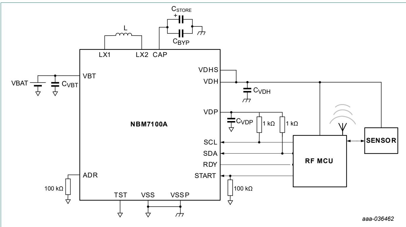
Fig. 51. Example application
Coin cell battery life booster with adaptive power optimization
Table 39. Design requirements
| Parameter | Values |
| Battery type | CR2032 |
| Input (battery) voltage | $2.4 \leq V_{VBT} \leq 3.0 \text{ V}$ |
| Regulated output voltage at VDH pin (Active state) | $1.8 \text{ V} \leq V_{\text{SET}} \leq 3.6 \text{ V}$ |
| Load profile current | up to 100 mA |
| Load profile duration | up to 200 ms |
| $V_{CAP(MAX)}$ | 11 V |
| Use optimizer | No |
| $C_{store}$ capacitor type | polymer |
11.3. DC-DC switching frequency and inductor selection
The internal DC-DC converter operates at a fixed frequency of approximately 1 MHz. It is not user adjustable. It is designed to operate with 15 $\mu$ H ( $\pm$ 20%, standard tolerance) and a saturation current rating of 1 A (minimum). Using an inductor with significantly different ratings may cause control loop instability.
Table 40. Recommended inductors
| Type number | L (μH) | DCR (mΩ) | saturation current | Size (l × w × h) mm | vendor |
| XGL4040-153ME | 15 | 80 | 1.2 | 4 × 4 × 4.1 | Coilcraft |
| SRN4018-150M | 15 | 264 | 1.1 | 4 × 4 × 1.8 | Bournes |
| 74404042150 | 15 | 210 | 1.4 | 4 × 3.3 × 1.8 | Wurth |
11.4. Output voltage setting, $V_{SET}$
The VDH output pin is regulated at the value of $V_{SET}$ during the active state. The default value is 3.0 V and may be adjusted in register 0x09[3:0]. Refer to Setting VDH output voltage, $V_{SET}$ (Active state).
11.5. Input capacitor, $C_{VBT}$ and charge current, $I_{CH}$ setting
During the charge state the DC-DC converter operates in boost mode. A constant current is drawn from the VBT pin according to the ich setting in register 0x10[7:5]. The capacitor ripple current is negligible and a 6.3V ceramic, 1 $\mu$ F (minimum) located close to the VBT pin is suggested.
The default charging current, $I_{CH}$ , is 8 mA. It can be adjusted in the set2 register 0x10[7:5] via the serial interface.
11.6. Output capacitors, $C_{VDP}$ and $C_{VDH}$
The VDP pin connects to VBT via an internal power switch in all states, except Active where it is connected to the regulated DC-DC output, VDH. The VDP output cannot be disabled via serial interface and as it is intended to supply always 'on' system loads of up to 10 mA. A 6.3V, 1 $\mu$ F ceramic located close to the VDP pin is suggested.
The VDH pin is the output of the DC-DC converter during an active cycle. To ensure stability and low output ripple under all DC-DC operating conditions, a derated capacitance of 22 $\mu$ F is recommended. Check manufacturer derating curves and select a suitable capacitor voltage rating to achieve the derated minimum. In this example, a 16 V, 22 $\mu$ F, X7R with $<\left|-10\right|%$ DC bias is chosen. The VDH output may be disabled when not in the Active state by setting vdhhiz = 1.
Coin cell battery life booster with adaptive power optimization
11.7. Storage capacitor, $C_{STORE}$
Sizing the energy storage capacitor depends on the worst case load profile required in the application. A suggested approach is to calculate the energy in $\mu J$ required to support the load pulse. The area under the curve gives a first order approximation of the minimum energy needed for the load, not considering conversion losses or leakage currents. See figure Fig. 37.
The type (ceramic, electrolytic, polymer, film, supercapacitor) of a single storage capacitor, or parallel combination of multiple capacitors used in an application depends on: PCB area available, volume available within the end-product enclosure, cost, etc. The critical factors in the final selection are: 1) a voltage rating higher than $V_{\mathrm{CAP(MAX)}}$ , and 2) an equivalent series resistance (ESR) less than 1 $\Omega$ .
- Area under pulse load portion of the curve (charge in microcoulombs). CHG = $t_{ON} \times I_{PK}$ in $\mu C$ . Where
a. $t_{ON}$ = duration of the load pulse in ms.
b. $I_{PK}$ = load pulse current in mA.
- Calculate the energy, E, in microjoules, $\mu J$ by multiplying above by $V_{SET}$ and add margin for energy conversion and leakage losses: 15 - 20%. Assume 20% as a starting point for a factor of 1.2.
E = charge × voltage = CHG × VSET × 1.2 in μJ.
- Calculate $\Delta V_{CSTORE} = (V_{CSTORE(high)} - V_{CSTORE(low)})$ , where
a. $V_{\text{CSTORE(low)}} = V_{\text{SET}} + 0.3 , \text{V}$ . Add 0.3 V, or greater, to the regulated $V_{SET}$ voltage to account for DC-DC dropout when the capacitor voltage depletes close to the regulation voltage.
b. $V_{CSTORE(high)} = V_{FIX}$ in 0x09[7:4], and $V_{FIX} \leq V_{CAP(MAX)}$ . See Section 8.4.2.3.
Calculate nominal $C_{STORE}$ capacitance in $\mu F$ : $C_{STORE} = (2 \times E) / (V_{CSTORE(high)}^{2} - V_{CSTORE(low)}^{2}) \mu F$
Apply appropriate voltage and temperature ratings based on storage capacitor type: Aluminum electrolytic, Aluminium polymer, ceramic, supercapacitor, etc.
Select standard value larger than calculated in step 4 with an ESR < 1 ohm and voltage rating larger than $V_{\mathrm{CAP(MAX)}}$ . Additional ceramic capacitors, $C_{BYP}$ may be used to decrease the effective ESR.
Test system under load profile used in step 1. Additional margin may be required to account for early warning response time and serial port communication from microcontroller. Iterate as necessary.
In this design example a load of 100 mA for 10 ms is chosen. Calculation steps show below:
CHG = 100 mA × 10 ms = 1000 μC
E = 1000 μC × 3.0 V × 1.2 = 4320 μJ (20% margin assumed in 1.2 multiplier)
a. $V_{CSTORE(low)} = V_{SET} + \text{margin } V = 3.0 , V + 0.5 , V$ (extra conservative) = 3.5 V
$$
V _ {C S T O R E (h i g h)} = V _ {\text { fix }} = V _ {C A P (M A X)} = 1 1 \mathrm{V}
$$
$$
C _ {C S T O R E (n o m)} = 2 \times 4 3 2 0 \mu J / (1 1 V ^ {2} - 3. 5 V ^ {2}) = 7 9. 4 \mu F
$$
Assume $C_{store}$ capacitor tolerance of $\pm 20 %$ (typical for an electrolytic). $C_{CSTORE(actual)} = 79.4 \mu F \times 1.2 = 95.3 \mu F$ .
Select a 16 V rated capacitor with closest standard value of 100 $\mu$ F.
Select 16 V (or higher) rated, low ESR parallel ceramic, $C_{BYP} = 10 \mu F$
11.8. External resistors
NBM7100A: I²C SCL and SDA pull-up resistors: consult with Table 12, the host controller data sheet and industry I²C specifications to size the SCL and SDA pin pullup resistors. For this application example, PCB trace capacitance, C $_{b}$ , is assumed to be < 400 pF, allowing Fast-mode Plus (1 Mbit/s) data transfer. 1 kΩ resistances as indicated in example application diagram are used as a compromise between signal integrity and power consumption.
NBM7100A ADR pin pullup or pull-down resistor: Refer to Table 18 for available slave addresses. For a '1' connect the ADR pin to the VDP pin via a pullup resistor. For '0' connect the ADR pin to the VSS pin with a pull-down resistor. A standard resistor value between 1kΩ and 100 kΩ is suggested, but can be omitted so long as a '1' or '0' electrical connection is made via PCB trace. A pull-down of 100 kΩ is chosen for this example.
NBM7100A: START pin resistor: To prevent spurious initiation of Auto mode during power-up or due to a high-Z condition from an external host, a pull-down resistor is recommended. The value of resistor should be low enough to ensure the START pin is held low when not being actively driven, and high enough to prevent loading the external host controller output when driven high. A pull-down of 100 kΩ is chosen for this example.
Coin cell battery life booster with adaptive power optimization
11.9. Suggestions for controlling NBM7100A/B via serial interface
At initialization:
Do not initiate any read or write sequences until at least 20 ms after the NBM7100A/B has completed power-on reset (battery insertion).
As required by the application after POR, update default registers as needed:
a. Write 0x0A: vmin, vdhhiz, ich.
b. Write 0x0B: vew, eew. Monitoring the early warning indication is suggested.
c. Write 0x0C: vcapmax.
d. Write 0x0D: opt_marg.
Initiating On-demand
Write 0x08 and 0x09: set prof number or use $V_{fix}$ .
Write 0x09: vset and vfix. vfix required if optimizer not used.
Write 0x08: set eod bit.
Monitor RDY pin with GPIO, or poll 0x00[0] for RDY = 1. When RDY = 1, $V_{DH} = V_{SET}$ .
Apply pulsed load and monitor RDY pin for ew, or continuously poll 0x00 for alrm, ew, and lowbat indications
a. If ew via RDY or 0x00, disable load, write 0x08[2:0] as 000b to enter standby. Capacitor is near depletion.
b. If alarm, disable load, write 0x08[2:0] as 000b to enter standby. The DC-DC is no longer able to regulate $V_{DH}$ due to overload or capacitor is near depletion.
c. If lowbat, battery is becoming depleted and needs replacement. Operation may continue.
Load pulse complete, write 0x08[2:0] as 000b to enter standby.
Repeat sequence for subsequent On-demand cycles.
Initiating Continuous
Write 0x08 and 0x09: set prof number or use $V_{FIX}$ .
Write 0x09: vset and vfix. vfix required if optimizer not used.
Write 0x08: set ecm bit.
Monitor RDY pin with GPIO, or poll 0x00[0] for RDY = 1.
When RDY = 1, Write 0x08[2] to enter active mode, $V_{DH} = V_{SET}$ .
- Apply pulsed load and monitor RDY pin for ew, or continuously poll 0x00 for alrm, ew, and lowbat indications
a. If ew via RDY or 0x00, disable load, write 0x08[2:0] as 000b to enter standby. Capacitor is near depletion.
b. If alarm, disable load, write 0x08[2:0] as 000b to enter standby. The DC-DC is no longer able to regulate $V_{DH}$ due to overload or capacitor is near depletion.
c. If lowbat, battery is becoming depleted and needs replacement. Operation may continue.
Load pulse complete, write 0x08[2:0] as 000b to enter standby; or 0x08[2:0] as 010b to return to Continuous mode.
Repeat sequence for subsequent Continuous mode cycles.
Coin cell battery life booster with adaptive power optimization
11.10. Application curves
$V_{VBT} = 3.0 , V; C_{VBT} = 1 , \mu F; C_{VDP} = 1 , \mu F; C_{VDH} = 22 , \mu F; L = 15 , \mu H;$ unless otherwise specified.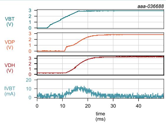
$V_{VBT}$ ramps from 0 to 3 V in 12.5 ms
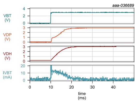
$V_{VBT}$ ramps from 0 to 3 V in 5 $\mu$ s
Fig. 52. POR (VBT slow ramp)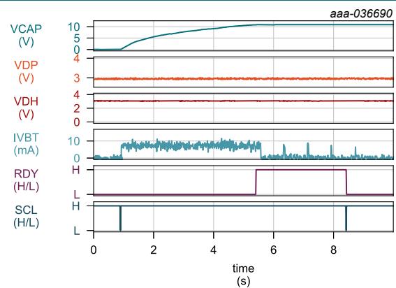
$$
V _ {V B T} = V _ {D P} = V _ {D H} = 3 \mathrm{V}
$$
$$
V _ {F I X} = 1 1 \mathrm{V}; I _ {C H} = 8 \mathrm{mA}
$$
Standby → Continuous → Standby
Fig. 53. POR (VBT fast ramp)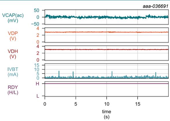
Fig. 54. Continuous mode
$$
V _ {V B T} = V _ {D P} = V _ {D H} = 3 \mathrm{V}
$$
$$
V _ {F I X} = 1 1 \mathrm{V}; I _ {C H} = 8 \mathrm{mA}
$$
Continuous mode: monitor, refresh, monitor
Fig. 55. Continuous mode with $V_{CAP}$ refresh pulses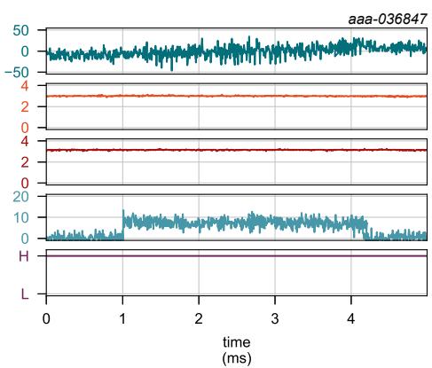
$$
V _ {V B T} = V _ {D P} = V _ {D H} = 3 \mathrm{V}
$$
$$
V _ {F I X} = 1 1 \mathrm{V}; I _ {C H} = 8 \mathrm{mA}
$$
Continuous mode: monitor, refresh, monitor
Fig. 56. Continuous mode with single $V_{CAP}$ refresh pulse, $V_{CAP}$ : AC coupled
Coin cell battery life booster with adaptive power optimization
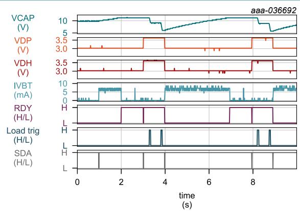
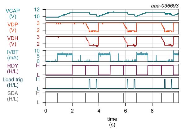
$$
\mathrm{VBT} = 3 \mathrm{V}; \mathrm{VDP} = \mathrm{VDH} = \mathrm{V} _ {\mathrm{SET}} = 3. 6 \mathrm{V}
$$
$$
V _ {F I X} = 1 1 \mathrm{V}
$$
$$
\mathrm{VBT} = 3 \mathrm{V}; \mathrm{VDP} = \mathrm{VDH} = \mathrm{V} _ {\mathrm{SET}} = 1. 8 \mathrm{V}
$$
$I_{LOAD} = 2 \times 50 , mA$ for 50 ms
$$
V _ {F I X} = 1 1 \mathrm{V}
$$
Load applied 1.25 sec after RDY = H, then at a 450 ms interval
$I_{LOAD} = 2 \times 50 , mA$ for 50 ms
Load applied 1.25 sec after RDY = H, then at a 450 ms interval
Fig. 57. Continuous to active mode transition ( $I_{VBT}$ )
Fig. 58. Continuous to active mode transition ( $I_{VBT}$ )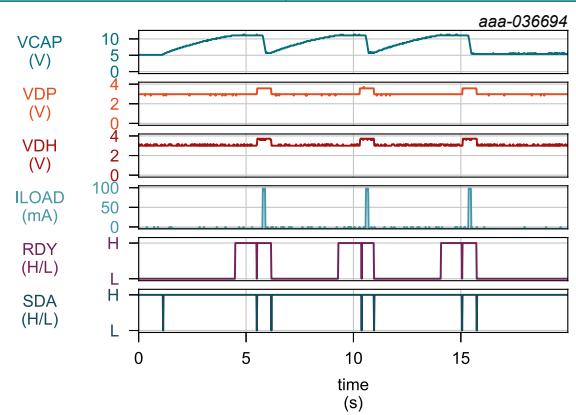
$$
\mathrm{VBT} = 3 \mathrm{V}; \mathrm{VDP} = \mathrm{VDH} = \mathrm{V} _ {\mathrm{SET}} = 3. 6 \mathrm{V}
$$
$$
V _ {F I X} = 1 1 \mathrm{V}
$$
$$
I _ {\text {LOAD}} = 1 0 0
$$
$$
\mathsf {R D Y} = \mathsf {H}
$$
Fig. 59. Continuous to active mode transition ( $I_{LOAD}$ )
Coin cell battery life booster with adaptive power optimization
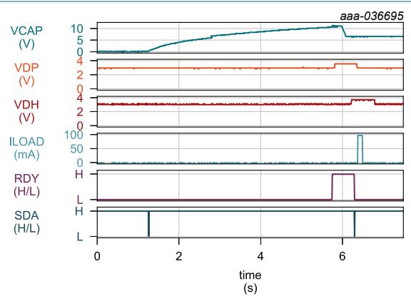
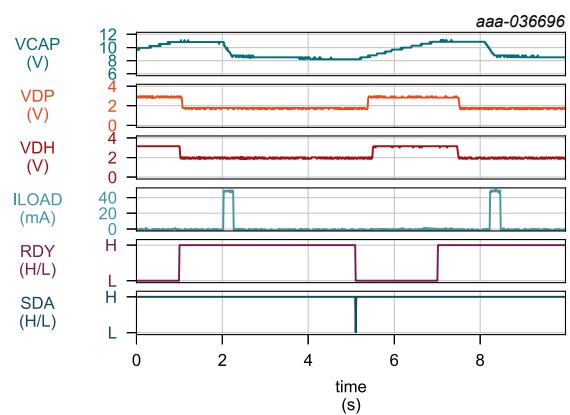
$$
V _ {V B T} = 3 \mathrm{V}; V _ {D P} = V _ {D H} = V _ {S E T} = 3. 6 \mathrm{V}
$$
$$
V _ {F I X} = 1 1 \mathrm{V}
$$
$$
V _ {V B T} = 3 \mathrm{V}; V _ {D P} = V _ {D H} = V _ {S E T} = 1. 8 \mathrm{V}
$$
$I_{LOAD} = 100 , mA$ for $100 , ms$
$$
V _ {F I X} = 1 1 \mathrm{V}
$$
Load applied 1.25 sec after RDY = H transition
$I_{LOAD} = 50 , mA$ for 200 ms
Load applied 1.25 sec after RDY = H transition
Fig. 60. On-demand to active mode transition ( $I_{LOAD}$ )
Fig. 61. On-demand to active mode transition ( $I_{LOAD}$ )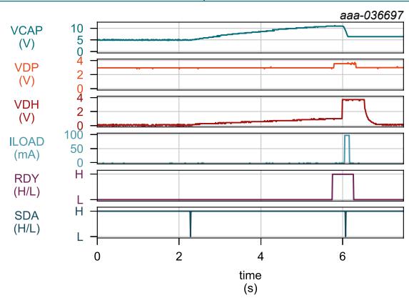
$$
V _ {B T} = 3 \mathrm{V}
$$
$$
V _ {D H} = V _ {S E T} = 3. 6 \mathrm{V}
$$
$$
V _ {F I X} = 1 1 \mathrm{V}
$$
$$
I _ {\text {LOAD}} = 1 0 0
$$
Fig. 62. On-demand to active mode transition (vdhhiz = 1)
Coin cell battery life booster with adaptive power optimization
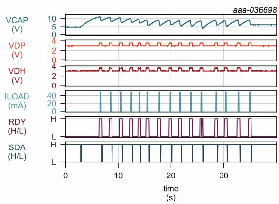
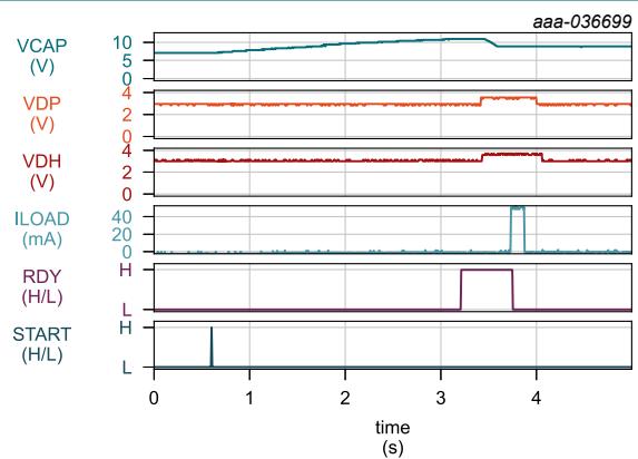
$$
V _ {V B T} = 3 \mathrm{V}; V _ {D P} = V _ {D H} = V _ {S E T} = 3. 6 \mathrm{V}
$$
$V_{VBT} = 3 \text{ V}; V_{DP} = V_{DH} = V_{SET} = 3.6 \text{ V}$ Optimizer profile 1 enabled, Opt margin = 'safe' (5.21 V) $V_{EW} = 4.8 \text{ V}$ $I_{LOAD} = 50 \text{ mA for } 100 \text{ ms (load pulses 1-10, 12-15)}$ $I_{LOAD} = 50 \text{ mA for } 130 \text{ ms (11th load), triggers EW (RDY briefly low)}$
$I_{LOAD} = 50 , mA$ for 100 ms
Fig. 63. Optimizer start, down regulation, Early Warning enabled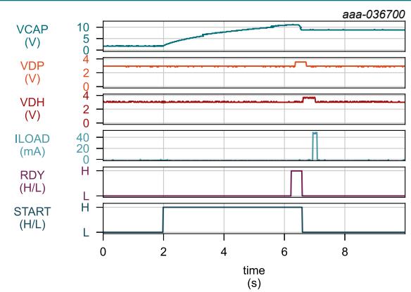
$$
V _ {V B T} = 3 \mathrm{V}; V _ {D P} = V _ {D H} = V _ {S E T} = 3. 6 \mathrm{V}
$$
$I_{LOAD} = 50 , mA$ for $100 , ms$
Fig. 64. Start pulse short - 10 μs (NBM7100A)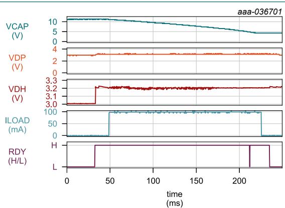
$$
V _ {V B T} = 3 \mathrm{V}; V _ {D P} = V _ {D H} = V _ {S E T} = 3. 2 \mathrm{V}
$$
Fig. 65. Start pulse long - 4.5 sec (NBM7100A)
$$
V _ {E W} = 4. 4 \mathrm{V}
$$
$I_{LOAD} = 100 , mA$ for $160 , ms$
Fig. 66. Load pulse - 0 to 100 mA, Early Warning enabled (NBM7100A)
11.11. Power supply recommendations
The device is designed to operate from a battery with a voltage range of 2.4 V to 5.5 V. $V_{VBT}$ should connect directly to the positive battery terminal with a bypass capacitor of $C_{VBT}$ (see Section 7.5). In most situations, using an input capacitance ( $C_{VBT}$ ) of 1 $\mu$ F is sufficient to prevent the supply voltage from dipping during device operation.
Coin cell battery life booster with adaptive power optimization
12. Layout
Layout guidelines
Improper layout can cause unstable operation, load regulation problems, increased ripple and noise. For best performance, all traces should be kept short.
The $C_{VBT}$ , $C_{VDH}$ , $C_{STORE}$ , and $C_{VDP}$ capacitors must be placed close to the device to minimize the effects that parasitic trace inductances may have on normal operation.
The DC-DC converter has two loops: boost mode from VBT to CAP and buck mode from CAP to VDH. For optimal performance, loop areas should be as small as possible.
Serial bus line routing is least critical, however, avoid running serial bus traces near or under the DC-DC converter loops.
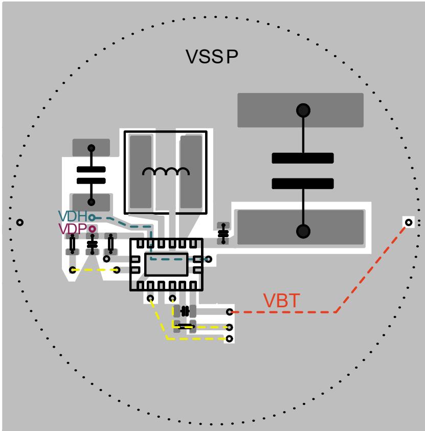
aaa-036460
Circle indicates CR2032 diameter
Fig. 67. layout example
Coin cell battery life booster with adaptive power optimization
13. Package information
13.1. Package outline
DHVQFN16: plastic dual in-line compatible thermal enhanced very thin quad flat package; no leads; 16 terminals; body 2.5 x 3.5 x 0.85 mm
SOT763-1
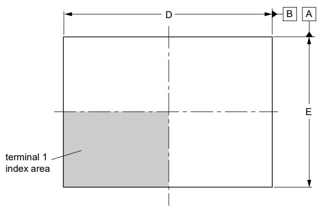
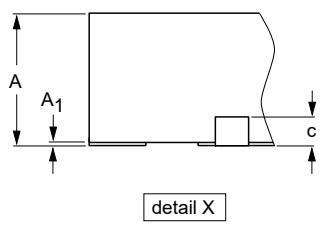
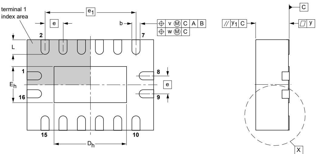

DIMENSIONS (mm are the original dimensions)
| UNIT | $A^{(1)}$ max. | $A_1$ | b | c | $D^{(1)}$ | $D_h$ | $E^{(1)}$ | $E_h$ | e | $e_1$ | L | v | w | y | $y_1$ |
| mm | 1 | 0.050.00 | 0.300.18 | 0.2 | 3.63.4 | 2.151.85 | 2.62.4 | 1.150.85 | 0.5 | 2.5 | 0.50.3 | 0.1 | 0.05 | 0.05 | 0.1 |
Note
- Plastic or metal protrusions of 0.075 mm maximum per side are not included.
| OUTLINE VERSION | REFERENCES | EUROPEAN PROJECTION | ISSUE DATE | |||
| IEC | JEDEC | JEITA | ||||
| SOT763-1 | --- | MO-241 | --- | -02-10-1703-01-27 | ||
Fig. 68. Package outline SOT763-1 (DHVQFN16)
Coin cell battery life booster with adaptive power optimization
14. Revision history
Table 41. Revision history
| Document ID | Release date | Data sheet status | Change notice | Supersedes |
| NBM7100 v.3 | 20250410 | Product data sheet | - | NBM7100 v.2 |
| Modifications: | Section 8.3, Section 8.4 and Section 11.9: several changes to the text where values were displayed in decimal instead of hexadecimal.Section 8.4.3: typo corrected for Buck mode (Active, 2nd phase); "SW1 and SW3 are ON".Section 8.4.4.1: typo corrected; "VDP connects to VDH via the VDP_to_VDH switch".Table 34: typo corrected; "Active states" changed to "Charge states". | |||
| NBM7100 v.2 | 20240802 | Product data sheet | - | NBM7100 v.1 |
| Modifications: | Table 7: added reference to JEDEC51-5 and -7.Table 10: 1) EFFch corrected; 2) IQ_ACT corrected.Fig. 50: figure corrected.Fig. 63: graph corrected. | |||
| NBM7100 v.1 | 20230629 | Product data sheet | - | - |
Coin cell battery life booster with adaptive power optimization
15. Legal information
Data sheet status
| Document status [1][2] | Product status [3] | Definition |
| Objective [short] data sheet | Development | This document contains data from the objective specification for product development. |
| Preliminary [short] data sheet | Qualification | This document contains data from the preliminary specification. |
| Product [short] data sheet | Production | This document contains the product specification. |
[1] Please consult the most recently issued document before initiating or completing a design.
[2] The term 'short data sheet' is explained in section "Definitions".
[3] The product status of device(s) described in this document may have changed since this document was published and may differ in case of multiple devices. The latest product status information is available on the internet at https://www.nexperia.com.
Definitions
Draft — The document is a draft version only. The content is still under internal review and subject to formal approval, which may result in modifications or additions. Nexperia does not give any representations or warranties as to the accuracy or completeness of information included herein and shall have no liability for the consequences of use of such information.
Short data sheet — A short data sheet is an extract from a full data sheet with the same product type number(s) and title. A short data sheet is intended for quick reference only and should not be relied upon to contain detailed and full information. For detailed and full information see the relevant full data sheet, which is available on request via the local Nexperia sales office. In case of any inconsistency or conflict with the short data sheet, the full data sheet shall prevail.
Product specification — The information and data provided in a Product data sheet shall define the specification of the product as agreed between Nexperia and its customer, unless Nexperia and customer have explicitly agreed otherwise in writing. In no event however, shall an agreement be valid in which the Nexperia product is deemed to offer functions and qualities beyond those described in the Product data sheet.
Disclaimers
Limited warranty and liability — Information in this document is believed to be accurate and reliable. However, Nexperia does not give any representations or warranties, expressed or implied, as to the accuracy or completeness of such information and shall have no liability for the consequences of use of such information. Nexperia takes no responsibility for the content in this document if provided by an information source outside of Nexperia.
In no event shall Nexperia be liable for any indirect, incidental, punitive, special or consequential damages (including - without limitation - lost profits, lost savings, business interruption, costs related to the removal or replacement of any products or rework charges) whether or not such damages are based on tort (including negligence), warranty, breach of contract or any other legal theory.
Notwithstanding any damages that customer might incur for any reason whatsoever, Nexperia's aggregate and cumulative liability towards customer for the products described herein shall be limited in accordance with the Terms and conditions of commercial sale of Nexperia.
Right to make changes — Nexperia reserves the right to make changes to information published in this document, including without limitation specifications and product descriptions, at any time and without notice. This document supersedes and replaces all information supplied prior to the publication hereof.
Suitability for use — Nexperia products are not designed, authorized or warranted to be suitable for use in life support, life-critical or safety-critical systems or equipment, nor in applications where failure or malfunction of an Nexperia product can reasonably be expected to result in personal injury, death or severe property or environmental damage. Nexperia and its suppliers accept no liability for inclusion and/or use of Nexperia products in such equipment or applications and therefore such inclusion and/or use is at the customer's own risk.
Quick reference data — The Quick reference data is an extract of the product data given in the Limiting values and Characteristics sections of this document, and as such is not complete, exhaustive or legally binding.
Applications — Applications that are described herein for any of these products are for illustrative purposes only. Nexperia makes no representation or warranty that such applications will be suitable for the specified use without further testing or modification.
Customers are responsible for the design and operation of their applications and products using Nexperia products, and Nexperia accepts no liability for any assistance with applications or customer product design. It is customer's sole responsibility to determine whether the Nexperia product is suitable and fit for the customer's applications and products planned, as well as for the planned application and use of customer's third party customer(s). Customers should provide appropriate design and operating safeguards to minimize the risks associated with their applications and products.
Nexperia does not accept any liability related to any default, damage, costs or problem which is based on any weakness or default in the customer's applications or products, or the application or use by customer's third party customer(s). Customer is responsible for doing all necessary testing for the customer's applications and products using Nexperia products in order to avoid a default of the applications and the products or of the application or use by customer's third party customer(s). Nexperia does not accept any liability in this respect.
Limiting values — Stress above one or more limiting values (as defined in the Absolute Maximum Ratings System of IEC 60134) will cause permanent damage to the device. Limiting values are stress ratings only and (proper) operation of the device at these or any other conditions above those given in the Recommended operating conditions section (if present) or the Characteristics sections of this document is not warranted. Constant or repeated exposure to limiting values will permanently and irreversibly affect the quality and reliability of the device.
Terms and conditions of commercial sale — Nexperia products are sold subject to the general terms and conditions of commercial sale, as published at http://www.nexperia.com/profile/terms, unless otherwise agreed in a valid written individual agreement. In case an individual agreement is concluded only the terms and conditions of the respective agreement shall apply. Nexperia hereby expressly objects to applying the customer's general terms and conditions with regard to the purchase of Nexperia products by customer.
No offer to sell or license — Nothing in this document may be interpreted or construed as an offer to sell products that is open for acceptance or the grant, conveyance or implication of any license under any copyrights, patents or other industrial or intellectual property rights.
Export control — This document as well as the item(s) described herein may be subject to export control regulations. Export might require a prior authorization from competent authorities.
Non-automotive qualified products — Unless this data sheet expressly states that this specific Nexperia product is automotive qualified, the product is not suitable for automotive use. It is neither qualified nor tested in accordance with automotive testing or application requirements. Nexperia accepts no liability for inclusion and/or use of non-automotive qualified products in automotive equipment or applications.
In the event that customer uses the product for design-in and use in automotive applications to automotive specifications and standards, customer (a) shall use the product without Nexperia's warranty of the product for such automotive applications, use and specifications, and (b) whenever customer uses the product for automotive applications beyond Nexperia's specifications such use shall be solely at customer's own risk, and (c) customer fully indemnifies Nexperia for any liability, damages or failed product claims resulting from customer design and use of the product for automotive applications beyond Nexperia's standard warranty and Nexperia's product specifications.
Translations — A non-English (translated) version of a document is for reference only. The English version shall prevail in case of any discrepancy between the translated and English versions.
Trademarks
Notice: All referenced brands, product names, service names and trademarks are the property of their respective owners.
Contents
- General description....1
- Features and benefits....1
- Applications....1
- Ordering information....2
- Marking....2
- Pin configuration and description....2
6.1. Pin configuration....2
6.2. Pin description....3 - Specifications....4
7.1. Limiting values....4
7.2. ESD ratings....4
7.3. Thermal information....4
7.4. Recommended operating conditions....4
7.5. Recommended components....5
7.6. Electrical characteristics....5
7.7. Dynamic characteristics....7
7.8. Typical characteristics....9
7.9. Timing diagrams....16
7.10. Test circuits....18 - Detailed description....19
8.1. Functional diagram....19
8.2. Overview....19
8.3. Operating modes....23
8.3.1. Mode overview....23
8.3.2. Continuous mode....24
8.3.3. On-demand mode....24
8.3.4. Auto mode (NBM7100A only)....24
8.4. Feature description....25
8.4.1. Chip control....25
8.4.2. States of operation....27
8.4.3. DC-DC converter....30
8.4.4. VDP and VDH output configuration....31
8.4.5. Adaptive power optimization....33
8.4.6. Fuel Gauge....36 - Register map....37
- Programming Tables....38
10.1. Status information....38
10.2. Mode controls....38
10.3. VDH Output voltage control (VSET)....39
10.4. Capacitor end-of-charge voltage (VFIX)....39
10.5. Capacitor maximum storage voltage (VCAP(MAX))....40
10.6. VBT pin minimum input voltage comparator threshold (VMIN)....40
10.7. Capacitor charge current (ICH)....40
Coin cell battery life booster with adaptive power optimization
10.8. CAP pin input voltage comparator Early Warning voltage ( $V_{EW}$ )....41
10.9. VDH switch configuration....41
10.10. Optimizer profile selection....41
10.11. Optimization margin voltage....42
10.12. Fuel gauge....42
10.13. Storage capacitor voltage status ( $V_{CAP}$ )....43
11. Application and implementation....44
11.1. Application information....44
11.2. Typical application....44
11.3. DC-DC switching frequency and inductor selection..45
11.4. Output voltage setting, $V_{SET}$ ....45
11.5. Input capacitor, $C_{VBT}$ and charge current, $I_{CH}$ setting....45
11.6. Output capacitors, $C_{VDP}$ and $C_{VDH}$ ....45
11.7. Storage capacitor, $C_{STORE}$ ....46
11.8. External resistors....46
11.9. Suggestions for controlling NBM7100A/B via serial interface....47
11.10. Application curves....48
11.11. Power supply recommendations....51
12. Layout....52
13. Package information....53
13.1. Package outline....53
14. Revision history....54
15. Legal information....55
© Nexperia B.V. 2025. All rights reserved
Figures and diagrams from the PDF
Preview the extracted datasheet assets and open any image in a separate tab for closer inspection.



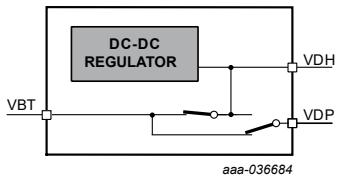
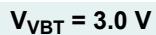

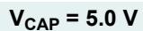
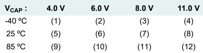
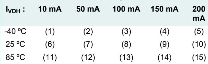
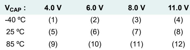

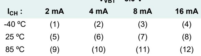
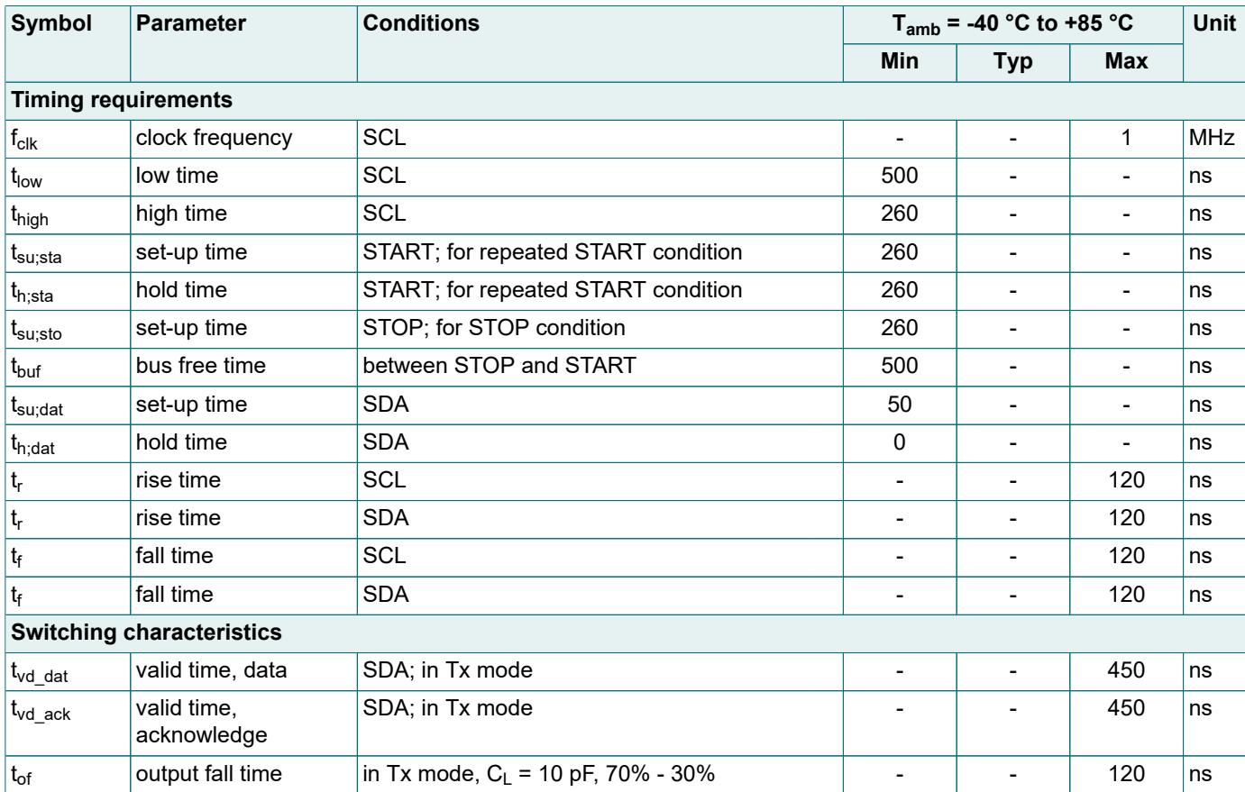
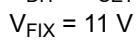
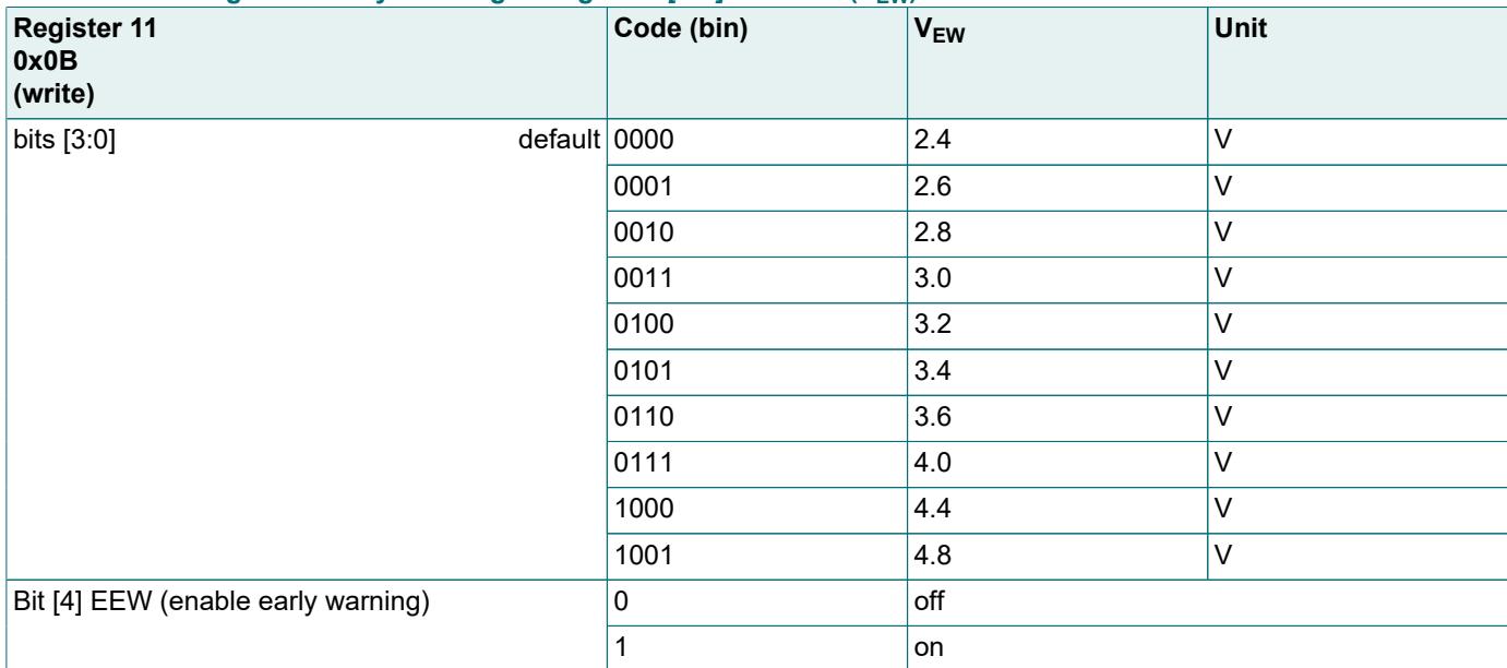
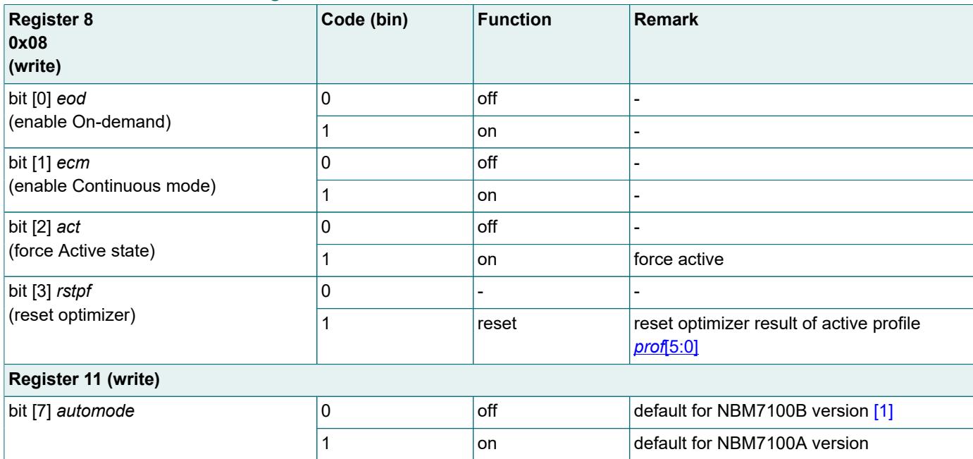
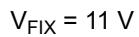

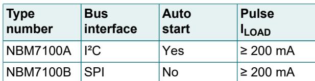


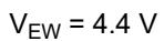

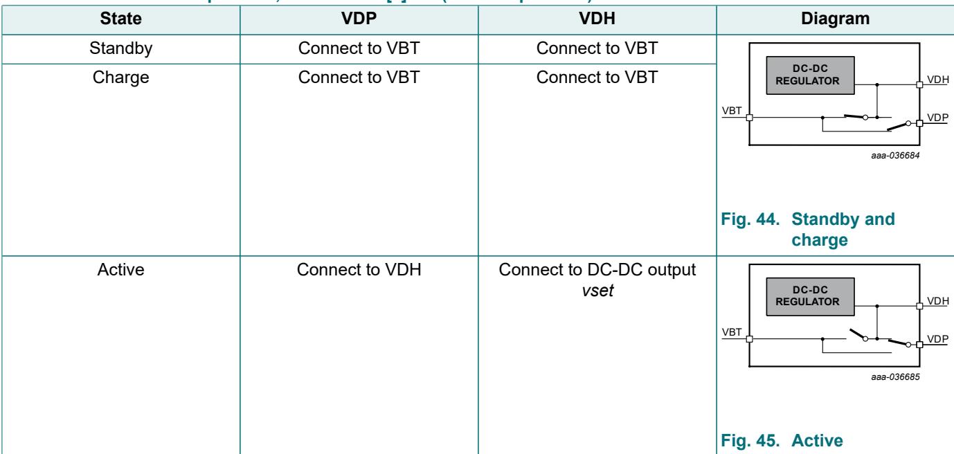



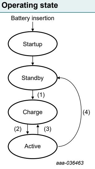

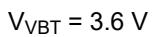
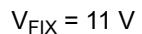




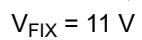

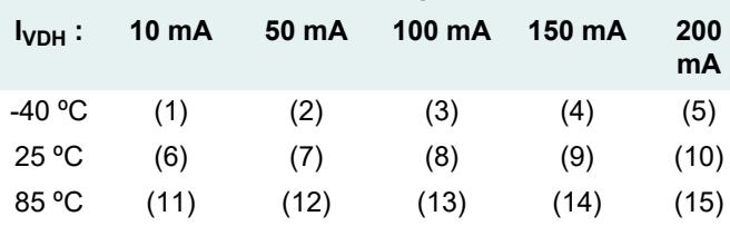
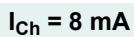
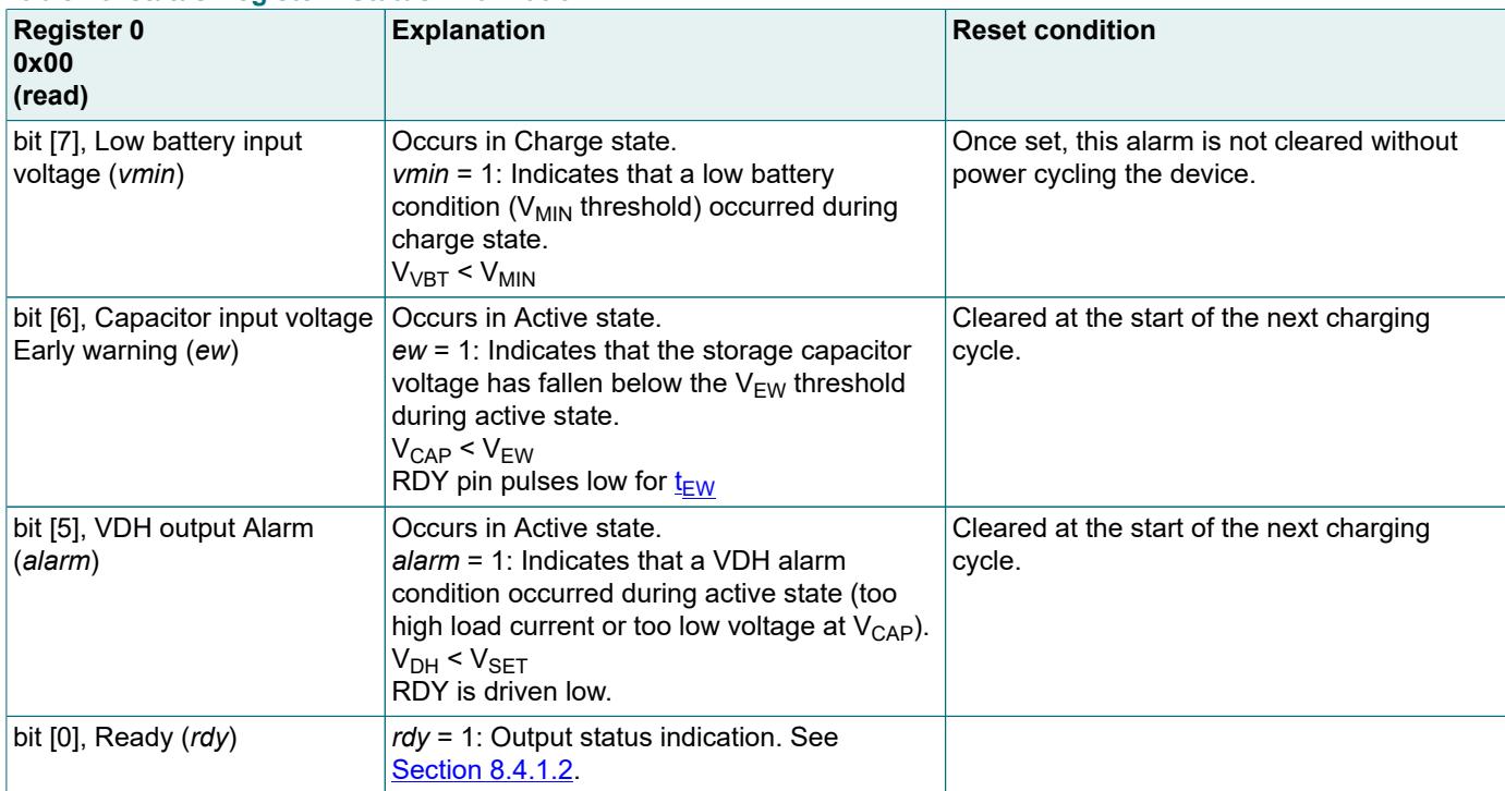
Use this datasheet from any agent
Send the page, markdown, chunks, or search endpoint to ChatGPT, Claude, embedr-app, or your own tooling.