
BMI160
Small, low power inertial measurement unit
BMI160 Small, low power inertial measurement unit
Bosch Sensortec

BOSCH
Invented for life
BMI160 – Data sheet
Document revision 1.0
Document release date
November 25th 2020
Document number
BST-BMI160-DS000-09
Technical reference code(s) 0 273 141 187
Notes
Data and descriptions in this document are subject to change without notice. Product photos and pictures are for illustration purposes only and may differ from the real product appearance.
BMI160 Small, low-power Inertial Measurement Unit
The BMI160 is a highly integrated, low power inertial measurement unit (IMU) that provides precise acceleration and angular rate (gyroscopic) measurement.
The BMI160 integrates:
16 bit digital, triaxial accelerometer
16 bit digital, triaxial gyroscope
Key features
High performance accelerometer and gyroscope (hardware synchronized)
Very low power consumption: typ. 925 µA (accelerometer and gyroscope in full operation)
Android Lollipop compatible: significant motion and step detector / step counter (5 µA each)
Very small 2.5 x 3.0 mm2 footprint, height 0.83 mm
Built-in power management unit (PMU) for advanced power management
Power saving with fast start-up mode of gyroscope
Wide power supply range: 1.71V … 3.6V
Allocatable FIFO buffer of 1024 bytes (capable of handling external sensor data)
Hardware sensor time-stamps for accurate sensor data fusion
Integrated interrupts for enhanced autonomous motion detection
Flexible digital primary interface to connect to host over I2C or SPI
Extended I2C mode with clock frequencies up to 1 MHz
Additional secondary high speed interface for OIS application
Capable of handling external sensor data
(e.g. geomagnetic or barometric pressure sensors by Bosch Sensortec)
Typical applications
Augmented Reality
Indoor navigation
3D scanning / indoor mapping
Advanced gesture recognition
Immersive gaming
9-axis motion detection
Air mouse applications and pointers
Pedometer / step counting
Advanced system power management for mobile applications
Optical image stabilization of camera modules
Free-fall detection and warranty logging
Target Devices
Smart phones, tablet and transformer PCs
Game controllers, remote controls and pointing devices
Head tracking devices
Wearable devices, e.g. smart watches or augmented reality glasses
Sport and fitness devices
Cameras, camera modules
Toys, e.g. toy helicopters
| BOSCH | BMI160Data sheet | Page 3 |
General Description
The BMI160 is an inertial measurement unit (IMU) consisting of a state-of-the-art 3-axis, low-g accelerometer and a low power 3-axis gyroscope. It has been designed for low power, high precision 6-axis and 9-axis applications in mobile phones, tablets, wearable devices, remote controls, game controllers, head-mounted devices and toys. The BMI160 is available in a compact 14-pin 2.5 × 3.0 × 0.83 mm3 LGA package. When accelerometer and gyroscope are in full operation mode, power consumption is typically 925 µA, enabling always-on applications in battery driven devices. The BMI160 offers a wide V voltage range from 1.71V to 3.6V and a V range from 1.2V to 3.6V, allowing the BMI160 to be powered at 1.8V for both V and V .
Due to its built-in hardware synchronization of the inertial sensor data and its ability to synchronize data of external devices such as geomagnetic sensors, BMI160 is ideally suited for augmented reality, gaming and navigation applications, which require highly accurate sensor data fusion. The BMI160 provides high precision sensor data together with the accurate timing of the corresponding data. The timestamps have a resolution of only 39 µs.
Further Bosch Sensortec sensors, e.g. geomagnetic (BMM150) can be connected as slave via a secondary I2C interface. In this configuration, the BMI160 controls the data acquisition of the external sensor and the synchronized data of all sensors is stored the register data and can be additionally stored in the built-in FIFO.
The integrated 1024 byte FIFO buffer supports low power applications and prevents data loss in non-real-time systems. The intelligent FIFO architecture allows dynamic reallocation of FIFO space for accelerometer, gyroscope and external sensors, respectively. For typical 6-DoF applications, this is sufficient for approx. 0.75 s of data capture. In a typical 9-DoF application – including the geomagnetic sensor – this is sufficient for approx. 0.5 s.
Like its predecessors, the BMI160 features an on-chip interrupt engine enabling low-power motion-based gesture recognition and context awareness. Examples of interrupts that can be issued in a power efficient manner are: any- or no-motion detection, tap or double tap sensing, orientation detection, free-fall or shock events. The BMI160 is Android 5.0 (Lollipop) compatible, and in the implementation of the Significant Motion and Step Detector interrupts, each consumes less than 30µA.
The smart built-in power management unit (PMU) can be configured, for example, to further lower the power consumption by automatically sending the gyroscope temporarily into fast start-up mode and waking it up again by internally using the any-motion interrupt of the accelerometer. By allowing longer sleep times of the host, the PMU contributes to significant further power saving on system level.
Besides the flexible primary interface (I2C or SPI) that is used to connect to the host, BMI160 provides an additional secondary interface. This secondary interface can be used in SPI mode for OIS (optical image stabilization) applications in conjunction with camera modules, or in advanced gaming use cases. When connected to a geomagnetic sensor, BMI160 will trigger autonomous read-out of the sensor data from magnetometer without the need for intervention by the host processor.
Index of Contents
- SPECIFICATION ....7
1.1 ELECTRICAL SPECIFICATION ....7
1.2 ELECTRICAL AND PHYSICAL CHARACTERISTICS, MEASUREMENT PERFORMANCE ....8
1.3 ABSOLUTE MAXIMUM RATINGS ....11 - FUNCTIONAL DESCRIPTION ....12
2.1 BLOCK DIAGRAM ....12
2.2 POWER MODES ....13
2.2.1 SUSPEND MODE (ACCELEROMETER AND GYROSCOPE) ....13
2.2.2 FAST START-UP MODE (GYROSCOPE ONLY) ....14
2.2.3 TRANSITIONS BETWEEN POWER MODES ....14
2.2.4 LOW POWER MODE (ACCELEROMETER ONLY) ....15
2.2.5 PMU (POWER MANAGEMENT UNIT) ....16
2.3 SENSOR TIMING AND DATA SYNCHRONIZATION ....18
2.3.1 SENSOR TIME ....18
2.3.2 DATA SYNCHRONIZATION ....18
2.4 DATA PROCESSING ....19
2.4.1 DATA PROCESSING ACCELEROMETER ....19
2.4.2 DATA PROCESSING GYROSCOPE ....21
2.5 FIFO ....21
2.5.1 FIFO FRAMES ....23
2.5.2 FIFO CONDITIONS AND DETAILS ....27
2.6 INTERRUPT CONTROLLER ....28
2.6.1 ANY-MOTION DETECTION (ACCEL) ....28
2.6.2 SIGNIFICANT MOTION (ACCEL) ....29
2.6.3 STEP DETECTOR (ACCEL) ....31
2.6.4 TAP SENSING (ACCEL) ....31
2.6.5 ORIENTATION RECOGNITION (ACCEL) ....32
2.6.6 FLAT DETECTION (ACCEL) ....38
2.6.7 LOW-G/FREE-FALL DETECTION (ACCEL) ....39
2.6.8 HIGH-G DETECTION (ACCEL) ....39
2.6.9 SLOW-MOTION ALERT/NO-MOTION INTERRUPT (ACCEL) ....40
2.6.10 DATA READY DETECTION (ACCEL, GYRO AND EXTERNAL SENSORS) ....43
2.6.11 PMU TRIGGER (GYRO) ....43
2.6.12 FIFO INTERRUPTS (ACCEL, GYRO, AND EXTERNAL SENSORS) ....43
2.7 STEP COUNTER ....44
2.8 DEVICE SELF TEST ....44
2.8.1 SELF-TEST ACCELEROMETER ....44
2.8.2 SELF-TEST GYROSCOPE ....45
2.9 OFFSET COMPENSATION ....45
2.9.1 FAST OFFSET COMPENSATION ....45
2.9.2 MANUAL OFFSET COMPENSATION ....46
2.9.3 INLINE CALIBRATION .... 46
2.10 NON-VOLATILE MEMORY .... 46
2.11 REGISTER MAP .... 48
2.11.1 REGISTER (0x00) CHIPID .... 50
2.11.2 REGISTER (0x02) ERR_REG .... 50
2.11.3 REGISTER (0x03) PMU_STATUS .... 51
2.11.4 REGISTER (0x04-0x17) DATA .... 52
2.11.5 REGISTER (0x18-0x1A) SENSORTIME .... 53
2.11.6 REGISTER (0x1B) STATUS .... 54
2.11.7 REGISTER (0x1C-0x1F) INT_STATUS .... 54
2.11.8 REGISTER (0x20-0x21) TEMPERATURE .... 56
2.11.9 REGISTER (0x22-0x23) FIFO_LENGTH .... 57
2.11.10 REGISTER (0x24) FIFO_DATA .... 58
2.11.11 REGISTER (0x40) ACC_CONF .... 58
2.11.12 REGISTER (0x41) ACC_RANGE .... 59
2.11.13 REGISTER (0x42) GYR_CONF .... 60
2.11.14 REGISTER (0x43) GYR_RANGE .... 61
2.11.15 REGISTER (0x44) MAG_CONF .... 61
2.11.16 REGISTER (0x45) FIFO_DOWNS .... 62
2.11.17 REGISTER (0x46-0x47) FIFO_CONFIG .... 63
2.11.18 REGISTER (0x4B-0x4F) MAG_IF .... 64
2.11.19 REGISTER (0x50-0x52) INT_EN.... 64
2.11.20 REGISTER (0x53) INT_OUT_CTRL.... 66
2.11.21 REGISTER (0x54) INT_LATCH.... 66
2.11.22 REGISTER (0x55-0x57) INT_MAP.... 67
2.11.23 REGISTER (0x58-0x59) INT_DATA.... 69
2.11.24 REGISTER (0x5A-0x5E) INT_LOWHIGH.... 70
2.11.25 REGISTER (0x5F-0x62) INT_MOTION.... 72
2.11.26 REGISTER (0x63-0x64) INT_TAP.... 74
2.11.27 REGISTER (0x65-0x66) INT_ORIENTATION.... 75
2.11.28 REGISTER (0x67-0x68) INT_FLAT.... 77
2.11.29 REGISTER (0x69) FOC_CONF.... 78
2.11.30 REGISTER (0x6A) CONF.... 78
2.11.31 REGISTER (0x6B) IF_CONF.... 79
2.11.32 REGISTER (0x6C) PMU_TRIGGER.... 79
2.11.33 REGISTER (0x6D) SELF_TEST.... 80
2.11.34 REGISTER (0x70) NV_CONF.... 81
2.11.35 REGISTER (0x71-0x77) OFFSET.... 81
2.11.36 REGISTER (0x78-0x79) STEP_CNT.... 82
2.11.37 REGISTER (0x7A-0x7B) STEP_CONF.... 83
2.11.38 REGISTER (0x7E) CMD.... 85
DIGITAL INTERFACES.... 88
3.1 INTERFACES.... 88
3.2 PRIMARY INTERFACE.... 88
3.2 Primary Interface I2C/SPI PROTOCOL SELECTION.... 89
3.2 Primary SPI INTERFACE.... 90
3.2 Primary I2C INTERFACE.... 93
3.2 Primary SPI AND I²C ACCESS RESTRICTIONS.... 97
3.3 SECONDARY INTERFACE.... 98
3.3 Primary MAGNETOMETER CONNECTED TO SECONDARY INTERFACE.... 98
3.3.2 CAMERA MODULE CONNECTED TO SECONDARY INTERFACE FOR OIS....100
4. PIN-OUT AND CONNECTION DIAGRAMS....101
4.1 PIN-OUT....101
4.2 CONNECTION DIAGRAMS TO USE PRIMARY INTERFACE ONLY....102
4.2.1 I²C AS PRIMARY INTERFACE....102
4.2.2 SPI 3-WIRE AS PRIMARY INTERFACE....102
4.2.3 SPI 4-WIRE AS PRIMARY INTERFACE....103
4.3 CONNECTION DIAGRAMS TO USE ADDITIONAL SECONDARY INTERFACE....103
4.3.1 PRIMARY SPI 4-WIRE AND SECONDARY MAGNETOMETER INTERFACE (I²C)....103
4.3.2 PRIMARY SPI 3-WIRE AND SECONDARY MAGNETOMETER INTERFACE (I²C)....104
4.3.3 PRIMARY I²C AND SECONDARY MAGNETOMETER INTERFACE (I²C)....104
4.3.4 PRIMARY I²C AND SECONDARY 4-WIRE SPI AS OIS INTERFACE....105
4.3.5 PRIMARY I²C AND SECONDARY 3-WIRE SPI AS OIS INTERFACE....105
5. PACKAGE....106
5.1 OUTLINE DIMENSIONS....106
5.2 SENSING AXES ORIENTATION....107
5.3 LANDING PATTERN RECOMMENDATION....108
5.4 MARKING....109
5.4.1 MASS PRODUCTION MARKING....109
5.4.2 ENGINEERING SAMPLES....109
5.5 SOLDERING GUIDELINES....110
5.6 HANDLING INSTRUCTIONS....111
5.7 TAPE AND REEL SPECIFICATION....111
5.7.1 ORIENTATION WITHIN THE REEL....112
5.8 ENVIRONMENTAL SAFETY....112
5.8.1 HALOGEN CONTENT....112
5.8.2 MULTIPLE SOURCING....112
6. LEGAL DISCLAIMER....113
6.1 ENGINEERING SAMPLES....113
6.2 PRODUCT USE....113
6.3 APPLICATION EXAMPLES AND HINTS....113
7. DOCUMENT HISTORY AND MODIFICATIONS....114
| BOSCH | BMI160Data sheet | Page 7 |
1. Specification
If not stated otherwise, the given values are over lifetime and full performance temperature and voltage ranges, minimum/maximum values are ±3. The specifications are split into accelerometer and gyroscope sections of the BMI160.
1.1 Electrical specification
VDD and VDDIO can be ramped in arbitrary order without causing the device to consume significant currents. The values of the voltage at VDD and the VDDIO pins can be chosen arbitrarily within their respective limits. The device only operates within specifications if the both voltages at VDD and VDDIO pins are within the specified range. The voltage levels at the digital input pins must not fall below GNDIO-0.3V or go above VDDIO+0.3V to prevent excessive current flowing into the respective input pin. BMI160 contains a brownout detector, which ensures integrity of data in the non-volatile memory under all operating conditions.
Table 1: Electrical parameter specification
| OPERATING CONDITIONS BMI160 | ||||||
| Parameter | Symbol | Condition | Min | Typ | Max | Unit |
| Supply Voltage Internal Domains | $V_{DD}$ | 1.71 | 3.0 | 3.6 | V | |
| Supply Voltage I/O Domain | $V_{DDIO}$ | 1.2 | 2.4 | 3.6 | V | |
| Voltage Input Low Level | $V_{IL,a}$ | SPI | $0.3V_{DDIO}$ | - | ||
| Voltage Input High Level | $V_{IH,a}$ | SPI | $0.7V_{DDIO}$ | - | ||
| Voltage Output Low Level | $V_{OL,a}$ | $V_{DDIO}=1.62V, I_{OL}=3mA, SPI$ | $0.2V_{DDIO}$ | - | ||
| $V_{DDIO}=1.2V, I_{OL}=3mA, SPI$ | $0.23V_{DDIO}$ | - | ||||
| Voltage Output High Level | $V_{OH,a}$ | $V_{DDIO}=1.62V, I_{OH}=3mA, SPI$ | $0.8V_{DDIO}$ | - | ||
| $V_{DDIO}=1.2V, I_{OH}=3mA, SPI$ | $0.62V_{DDIO}$ | - | ||||
| Operating Temperature | $T_A$ | -40 | +85 | °C | ||
| NVM write-cycles | $n_{NVM}$ | Non-volatile memory | 14 | Cycles | ||
| Current consumption | $I_{DD}$ | Gyro in fast start-up, accel in suspend mode, $T_A=25°C$ | 500 | 600 | μA | |
| Gyro and accel full operation mode, $T_A=25°C$ | 925 | 990 | ||||
| Gyro full operation mode, accel in suspend, $T_A=25°C$ | 850 | 900 | ||||
| Accel full operation mode, gyro in suspend, $T_A=25°C$ | 180 | 300 | ||||
| Gyro and accel in suspend mode, $T_A=25°C$ | 3 | 10 | ||||
| Significant motion detector, gyro in suspend, accel in low power mode @50Hz, TA=25°C | 30 | |||||
| Step detector, gyro in suspend, accel in low power mode @50Hz, TA=25°C | 30 | |||||
| BOSCH | BMI160Data sheet | Page 8 |
1.2 Electrical and physical characteristics, measurement performance
Table 2: Electrical characteristics accelerometer
| OPERATING CONDITIONS ACCELEROMETER | ||||||
| Parameter | Symbol | Condition | Min | Typ | Max | Units |
| Acceleration Range | $g_{FS2g}$ | Selectable via serial digital interface | ±2 | g | ||
| $g_{FS4g}$ | ±4 | g | ||||
| $g_{FS8g}$ | ±8 | g | ||||
| $g_{FS16g}$ | ±16 | g | ||||
| Start-up time | $t_{A,su}$ | Suspend/low power mode to normal mode, ODR=1.6kHz | 3.2 | 3.8 | ms | |
| OUTPUT SIGNAL ACCELEROMETER | ||||||
| Parameter | Symbol | Condition | Min | Typ | Max | Units |
| Resolution | 16 | bit | ||||
| Sensitivity | $S_{2g}$ | $g_{FS2g}, T_A=25°C$ | 15729 | 16384 | 17039 | LSB/g |
| $S_{4g}$ | $g_{FS4g}, T_A=25°C$ | 7864 | 8192 | 8520 | LSB/g | |
| $S_{8g}$ | $g_{FS8g}, T_A=25°C$ | 3932 | 4096 | 4260 | LSB/g | |
| $S_{16g}$ | $g_{FS16g}, T_A=25°C$ | 1966 | 2048 | 2130 | LSB/g | |
| Sensitivity Temperature Drift | $TCS_A$ | $g_{FS8g}, Nominal V_{DD} supplies best fit straight line$ | ±0.03 | %/K | ||
| Sensitivity change over supply voltage | $S_{A,VDD}$ | $T_A=25°C, V_{DD,min} ≤ V_{DD} ≤ V_{DD,max} best fit straight line$ | 0.01 | %/V | ||
| Zero-g Offset | $Off_{A,init}$ | $g_{FS8g}, T_A=25°C, nominal V_{DD} supplies, component level$ | ±25 | mg | ||
| $Off_{A,board}$ | $g_{FS8g}, T_A=25°C, nominal V_{DD} supplies, soldered, board level$ | ±40 | mg | |||
| $Off_{A,MSL}$ | $g_{FS8g}, T_A=25°C, nominal V_{DD} supplies, after MSL1-prec.\( ^1$ /soldered | ±70 | mg | |||
| $Off_{A,life}$ | $g_{FS8g}, T_A=25°C, nominal V_{DD} supplies, soldered, over life time^2$ | ±150 | mg | |||
| Zero-g Offset Temperature Drift | $TCO_A$ | $g_{FS8g}, Nominal V_{DD} supplies best fit straight line$ | ±1.0 | mg/K | ||
| Nonlinearity | $NL_A$ | Best fit straight line, $g_{FS8g}$ | ±0.5 | %FS | ||
| Output Noise | $n_{A,nd}$ | $g_{FS8g}, T_A=25°C, nominal V_{DD}, Normal mode$ | 180 | 300 | μg/√Hz | |
| BOSCH | BMI160Data sheet | Page 9 |
| $n_{A,rms}$ | Filter setting 80 Hz, ODR 200 Hz | 1.8 | mg-rms | |||
| Cross Axis Sensitivity | $S_A$ | Relative contribution between any two of the three axes | 1 | % | ||
| Alignment Error | $E_A$ | Relative to package outline | ±0.5 | ° | ||
| Output Data rate (set of x,y,z rate) | $ODR_A$ | 12.5 | 1600 | Hz | ||
| Output Data rate accuracy (set of x,y,z rate) | $AODR_A$ | Normal mode, over whole operating temperature range | ±1 | % |
Table 3: Electrical characteristics gyroscope
| OPERATING CONDITIONS GYROSCOPE | ||||||
| Parameter | Symbol | Condition | Min | Typ | Max | Unit |
| Range | $R_{FS125}$ | Selectable via serial digital interface | 125 | %s | ||
| $R_{FS250}$ | 250 | %s | ||||
| $R_{FS500}$ | 500 | %s | ||||
| $R_{FS1000}$ | 1,000 | %s | ||||
| $R_{FS2000}$ | 2,000 | %s | ||||
| Start-up time | $t_{G,su}$ | Suspend to normal mode ODRG=1600Hz | 55 | ms | ||
| $t_{G,FS}$ | Fast start-up to normal mode | 10 | ms | |||
| OUTPUT SIGNAL GYROSCOPE | ||||||
| $R_{FS2000}$ | Ta=25°C | 15.9 | 16.4 | 16.9 | LSB/°/s | |
| $R_{FS1000}$ | Ta=25°C | 31.8 | 32.8 | 33.8 | LSB/°/s | |
| Sensitivity | $R_{FS500}$ | Ta=25°C | 63.6 | 65.6 | 67.6 | LSB/°/s |
| $R_{FS250}$ | Ta=25°C | 127.2 | 131.2 | 135.2 | LSB/°/s | |
| $R_{FS125}$ | Ta=25°C | 254.5 | 262.4 | 270.3 | LSB/°/s | |
| Sensitivity change over temperature | $TCS_G$ | $R_{FS2000}$ , Nominal $V_{DD}$ supplies best fit straight line | ±0.02 | %/K | ||
| Sensitivity change over supply voltage | $S_G,V_{DD}$ | $T_A=25°C, V_{DD,min} \leqslant V_{DD} \leqslant V_{DD,max}$ best fit straight line | 0.01 | %/V | ||
| Nonlinearity | $NL_G$ | Best fit straight line $R_{FS1000}, R_{FS2000}$ | 0.1 | %FS | ||
| g- Sensitivity | Sensitivity to acceleration stimuli in all three axis (frequency <20kHz) | 0.1 | °/s/g | |||
| Zero-rate offset | Off $\Omega_x$ $\Omega_y$ and $\Omega_z$ | $T_A=25°C,$ fast offset compensation off | ±3 | °/s | ||
BST-BMI160-DS000-09 | Revision 1.0 | November 2020
| BOSCH | BMI160Data sheet | Page 10 | ||||
| Zero-Rate offset Over temperature | Off $\Omega_{x, oT}$ $\Omega_{y, oT}$ and $\Omega_{z, oT}$ | -40°C ≤ $T_A$ ≤+85°C | ±3 | %s | ||
| Zero-rate offset change over temperature | TCOG | -40°C ≤ $T_A$ ≤+85°C,best fit straight line | 0.05 | %s/K | ||
| Output Noise | $n_{G,nD}$ | @10 Hz | 0.007 | %s/ $\sqrt{Hz}$ | ||
| $n_{G,rms}$ | Filter setting 74.6Hz, ODR 200 Hz | 0.07 | %s rms | |||
| Output Data Rate (set of x,y,z rate) | ODRG | 25 | 3200 | Hz | ||
| Output Data rate accuracy (set of x,y,z rate) | AODRG | Over whole operating temperature range | ±1 | % | ||
| Cross Axis Sensitivity | $X_{G,S}$ | Sensitivity to stimuli in non-sense-direction | 2 | % | ||
Table 4: Electrical characteristics temperature sensor
| OPERATING CONDITIONS AND OUTPUT SIGNAL OF TEMPERATURE SENSOR | ||||||
| Parameter | Symbol | Condition | Min | Typ | Max | Unit |
| Temperature Sensor Measurement Range | $T_{S}$ | -40 | 85 | °C | ||
| Temperature Sensor Slope | $dT_{S}$ | 0.002 | K/LSB | |||
| Temperature Sensor Offset | $OT_{S}$ | ±2 | K | |||
| Output Data Rate | $ODR_{T}$ | Accelerometer on or gyro in fast start-up | 0.8 | Hz | ||
| Gyro active | 100 | Hz | ||||
| Resolution | $n_{T}$ | Accelerometer on or gyro in fast start-up | 8 | bit | ||
| Gyro active | 16 | bit | ||||
1.3 Absolute maximum ratings
Table 5: Absolute maximum ratings
| Parameter | Condition | Min | Max | Units |
| Voltage at Supply Pin | $V_{DD}$ Pin | -0.3 | 4.25 | V |
| $V_{DDIO}$ Pin | -0.3 | 4.25 | V | |
| Voltage at any Logic Pin | Non-Supply Pin | -0.3 | $V_{DDIO}+0.3$ | V |
| Passive Storage Temp. Range | ≤65% rel. H. | -50 | +150 | °C |
| None-volatile memory (NVM) Data Retention | T = 85°C, after 15 cycles | 10 | y | |
| Mechanical Shock | Duration 200 μs, half sine | 10,000 | g | |
| Duration 1.0 ms, half sine | 2,000 | g | ||
| Free fall onto hard surfaces | 1.8 | m | ||
| ESD | HBM, at any Pin | 2 | kV | |
| CDM | 500 | V | ||
| MM | 200 | V |
Note: Stresses above these listed maximum ratings may cause permanent damage to the device. Exposure beyond specified electrical characteristics as specified in Table 1 may affect device reliability or cause malfunction.
| BOSCH | BMI160Data sheet | Page 12 |
2. Functional Description
2.1 Block diagram
The figure below depicts the dataflow in BMI160 and the configuration parameters for data rates:

Figure 1: Block diagram of data flow
The pre-filtered input data may be already temperature compensated or other low level correction operations may be applied to them.
The data from the sensor are always sampled with a data rate of 6400 Hz for the gyroscope and 1600 Hz for the accelerometer. The data are filtered to an output data rate configured in the Register (0x40) ACC_CONF and Register (0x42) GYR_CONF for accelerometer and gyroscope, respectively. The data processing implements a low pass filter configured in the Register (0x40) ACC_CONF and Register (0x42) GYR_CONF for accelerometer and gyroscope, respectively. In addition further down sampling for the interrupt engines and the FIFO is possible and configured in the Register (0x45) FIFO_DOWNS. This down sampling discards data frames. The sensor time is synchronized with the update of the data register. Synchronization is a purely digital statement.
| BOSCH | BMI160Data sheet | Page 13 |
2.2 Power modes
By default BMI160 accel and gyro are in suspend mode after powering up the device. The device is powering up in less than 10ms.
Three power modes are supported for accelerometer and gyroscope:
Accelerometer
Normal mode: full chip operation
Low power mode: duty-cycling between suspend and normal mode. FIFO data readout are supported in lower power mode to a limited extent, see Register PMU_STATUS.
Suspend mode: No sampling takes place, all data is retained, and delays between subsequent I2C operations are allowed. FIFO data readout is not supported in suspend mode.
Gyroscope
Normal mode: same as accelerometer
Suspend mode: same as accelerometer
Fast start-up mode: start-up delay time to normal mode ≤10 ms
Table 6: Power modes of accelerometer and gyro in BMI160
| Accelerometer | Gyroscope | external Magnetometer BMM150 | ||
| full operation mode | Normal mode | ✓ | ✓ | ✓ |
| Sleep modes | Fast Start-up mode | ✓ | ||
| Suspend mode | ✓ | ✓ | ✓ | |
| Low power modes | Low power mode | ✓ | ✓ |
Suspend and fast start-up modes are sleep modes. Switching between normal and low power mode will not impact the output data from the sensor. This allows the system to switch from low power mode to normal mode to read out the sensor data in the FIFO with a data rate limited by the serial interface.
2.2.1 Suspend mode (accelerometer and gyroscope)
In suspend mode, the MEMS sensors are powered off but the digital circuitry is still active.
Note:
When all sensors are in suspend or low power mode, burst writes are not supported, normal writes need wait times after the write command is issued (~400 µs), and burst reads are not supported on Register (0x24) FIFO_DATA. If all sensors (accelerometer, gyroscope or magnetometer) are in either suspend or low power mode, the FIFO must not be read.
| BOSCH | BMI160Data sheet | Page 14 |
2.2.2 Fast start-up mode (gyroscope only )
In fast start-up mode the sensing analog part is powered down, while the drive and the digital part remains largely operational. No data acquisition is performed. The latest rate data and the content of all configuration registers are kept. The fast start-up mode allows a fast transition (≤10 ms) into normal mode while keeping power consumption significantly lower than in normal mode.
2.2.3 Transitions between power modes
The table below for the power modes of gyroscope and accelerometer shows which power mode combinations are supported by BMI160.
With regard to the below diagram, transitions between power modes are only allowed in horizontal or vertical direction. Transitions in diagonal direction are not supported.
Table 7: Typical total current consumption in µA according to accel/gyro modes
| Current consumption in μA | Accelerometer Mode | |||
| Suspend | Normal | Low Power | ||
| Gyroscope Mode | Suspend | 3 | 180 | See Table 8 |
| Fast Start-up | 500 | 580 | n.a. | |
| Normal | 850 | 925 | n.a. | |
The power mode setting can be configures independently from the output data rate set. The main difference between normal and low power mode is the power consumption as shown in the figure below. If the sleep time between two configured sampling intervals becomes too short to duty cycle between suspend and normal mode, the accelerometer stays automatically in normal mode. In order to make the transition between low power and normal mode as transparent as possible, an undersampling mode is defined in such a way that it mimics the behavior of the lower data rate in low power mode in normal mode. The low power mode then only switches clock sources.

Figure 2: low power and normal mode operation
2.2.4 Low power mode (accelerometer only)
In low power modes the accelerometer toggles between normal mode and suspend mode. The power consumption is given by the power consumption in normal mode times the fraction of time the sensor is in normal mode. The time in normal mode is defined by the startup time of the MEMS element, plus the analogue settling time. This results in a minimum time in normal mode of the settling time plus (averaged samples)/1600 Hz.
Regarding register read and write operations, the note in chapter 2.2.1 applies.
2.2.4.1 Power Consumption in accelerometer low power mode
When accelerometer and gyroscope are operated in normal mode, there is no significant dependence on the specific settings like ODR, undersampling and bandwidth. The same applies to the fast power up mode of the gyroscope. If the accelerometer, however, is operated in low power mode and undersampling is enabled, the power consumption of the accel depends on the two parameters ODR and number of averaging cycles.
In low power mode (gyroscope in suspend), the actual power consumption depends on the selected setting in Register (0x40) ACC_CONF.
Table 8: Typical total current consumption in µA according to number of averaging cycles and accelerometer ODR settings (gyroscope in suspend mode and accelerometer in low power mode and undersampling)
| Typical current consumption in μA | AVG – number of averaging cycles | ||||||||
| 1 | 2 | 4 | 8 | 16 | 32 | 64 | 128 | ||
| ODR of accelerometer in low power mode [Hz] (gyroscope in suspend mode) | 0.78125 | 3 | 3 | 4 | 4 | 5 | 6 | 9 | 14 |
| 1.5625 | 4 | 4 | 4 | 5 | 6 | 9 | 14 | 25 | |
| 3.125 | 4 | 5 | 5 | 7 | 9 | 15 | 25 | 46 | |
| 6.25 | 6 | 6 | 8 | 10 | 16 | 26 | 47 | 90 | |
| 12.5 | 8 | 10 | 12 | 18 | 28 | 49 | 92 | n. m.* | |
| 25 | 14 | 17 | 22 | 32 | 54 | 96 | normal mode* | ||
| 50 | 25 | 30 | 41 | 62 | 104 | normal mode* | |||
| 100 | 46 | 57 | 78 | 121 | normal mode* | ||||
| 200 | 90 | 111 | 154 | normal mode* | |||||
| 400 | 172 | 172 | normal mode* | ||||||
| 800 | normal mode* | ||||||||
| 1600 | normal mode* | ||||||||
* Note: Those combinations are not available in low-power mode. Cycling in suspend is not possible. Pls. switch to normal power mode for these combinations.
2.2.4.2 Noise of accelerometer in low power mode
When acc_us=1, accelerometer is in undersampling mode. The noise is only depending on the number of averaging cycles
Table 9: Accel noise in mg according to averaging with undersampling (range +/- 8g)
| AVG – number of averaging cycles | 1 | 2 | 4 | 8 | 16 | 32 | 64 | 128 |
| RMS-noise (typ.) [mg] X, Y | 5.2 | 3.6 | 2.5 | 1.8 | 1.3 | 0.9 | 0.6 | 0.5 |
| RMS-noise (typ.) [mg] Z | 3.7 | 3.2 |
2.2.5 PMU (Power Management Unit)
The integrated PMU (Power Management Unit) allows advanced power management features by combining power management features of all built-in sensors and externally available wake-up devices.
See chapter 2.6.11, PMU Trigger (Gyro).
2.2.5.1 Automatic gyroscope power mode changes
To further lower the power consumption, the gyroscope may be configured to be temporarily put into sleep mode, which is in BMI160 configurable as suspend or fast-start-up mode, when no motion is detected by the accelerometer. This mode benefits from the accelerometer any-motion and nomotion interrupt that is used to control the power state of the gyroscope. To configure this feature Register (0x6C) PMU_TRIGGER is used.
| BOSCH | BMI160Data sheet | Page 17 |
2.2.5.2 Power management with external geomagnetic sensor
An external magnetometer can be connected via the secondary interface. The drivers support Bosch Sensortec devices. The PMU allows advanced power management with the external magnetometer.
Table 10: Supported magnetometer and accelerometer power modes (only horizontal and vertical transitions are allowed)
| Accel | ||||
| Suspend | Normal | Low power | ||
| Magnetometer | Suspend | Supported | Supported | Supported |
| Normal | Supported | Supported | Supported | |
Note, for setting the magnetometer to suspend mode it is required to put the magnetometer itself into suspend mode through the magnetometer interface manual mode mag_man_en in Register (0x4B-0x4F) MAG_IF and to set the magnetometer interface after that to suspend using a mag_set_pmu_mode command in the Register (0x7E) CMD. Changing the magnetometer interface power mode to suspend does not imply any mode change in the magnetometer.
| BOSCH | BMI160Data sheet | Page 18 |
2.3 Sensor Timing and Data synchronization
2.3.1 Sensor Time
The Register (0x18-0x1A) SENSORTIME is a free running counter, which increments with a resolution of 39 µs. All sensor events e.g. updates of data registers are synchronous to this register as defined in the table below. With every update of the data register or the FIFO, a bit m in the Register (0x18-0x1A) SENSORTIME toggles where m depends on the output data rate for the data register and the output data rate and the FIFO down sampling rate for the FIFO. The table below shows which bit toggles for which update rate of data register and FIFO. The time stamps in Register (0x18-0x1A) SENSORTIME are available independent of the power mode the device is in.
Table 11: Sensor time
| Bit m in sensor_time | Resolution [ms] | Update rate [Hz] |
| 0 | 0.039 | 25641 |
| 1 | 0.078 | 12820 |
| 2 | 0.156 | 6400 |
| 3 | 0.3125 | 3200 |
| 4 | 0.625 | 1600 |
| 5 | 1.25 | 800 |
| 6 | 2.5 | 400 |
| 7 | 5 | 200 |
| 8 | 10 | 100 |
| 9 | 20 | 50 |
| 10 | 40 | 25 |
| 11 | 80 | 12.5 |
| 12 | 160 | 6.25 |
| 13 | 320 | 3.125 |
| 14 | 640 | 1.56 |
| 15 | 1280 | 0.78 |
| 16 | 2560 | 0.39 |
| 17 | 5120 | 0.20 |
| 18 | 10240 | 0.10 |
| 19 | 20480 | 0.049 |
| 20 | 40960 | 0.024 |
| 21 | 81920 | 0.012 |
| 22 | 163840 | 0.0061 |
| 23 | 327680 | 0.0031 |
2.3.2 Data synchronization
The sensor data from accelerometer and gyroscope are strictly synchronized on hardware level, i.e. they run on exactly the same sampling rate.
BMI160 supports various level of data synchronization:
Internal hardware synchronization of accelerometer, gyroscope and external sensor data.
| BOSCH | BMI160Data sheet | Page 19 |
Hardware synchronization of the data of accelerometer, gyro and external sensor through a unique DRDY interrupt signal.
FIFO entries of the accelerometer, gyro and external sensor are already synchronized by hardware. The according time stamp can be provided with each full FIFO read.
Synchronization of external data (e.g. magnetometer data) with FIFO data at data sampling granularity through hardware signaling
2.4 Data Processing
The accelerometer digital filter can be configured through the parameters: acc_bwp, acc_odr and acc_us. The gyroscope digital filter can be configured through the parameters: gyr_bwp and gyr_odr. There is no undersampling parameter for the gyroscope.
Note:
Illegal settings in configuration registers will result in an error code in the Register (0x02) ERR_REG. The content of the data register is undefined, and if the FIFO is used, it may contain no value.
2.4.1 Data Processing Accelerometer
The accelerometer digital filter can be configured through the parameters: acc_bwp, acc_odr and acc_us in Register (0x40) ACC_CONF for the accelerometer. The accelerometer data can only be processed in normal power mode or in low power mode.
2.4.1.1 Accelerometer data processing for normal power mode
When normal power mode is used, the undersampling mode should be disabled (acc_us=0b0). In this configuration mode, the accelerometer data is sampled at equidistant points in the time, defined by the accelerometer output data rate parameter (acc_odr). The output data rate can be configured in one of eight different valid ODR configurations going from 12.5Hz up to 1600Hz.
Note: Lower ODR values than 12.5Hz are not allowed when undersampling mode is not enabled. If they are used they result in an error code in Register (0x02) ERR_REG.
When acc_us=0b0, the acc_bwp parameter needs to be set to 0b010 (normal mode). The filter bandwidth shows a 3db cutoff frequency shown in the following table:
Table 12: 3dB cutoff frequency of the accelerometer according to ODR with normal filter mode
| Accelerometer ODR [Hz] | 12.5 | 25 | 50 | 100 | 200 | 400 | 800 | 1600 |
| 3dB Cutoff frequency [Hz] | 5.06 | 10.12 | 20.25 | 40.5 | 80 | 162(155 for Z axis) | 324(262 for Z axis) | 684(353 for Z axis) |
The noise is also depending on the filter settings and ODR, see table below.
| BOSCH | BMI160Data sheet | Page 20 |
Table 13: Accelerometer noise in mg according to ODR with normal filter mode (range +/- 8g)
| ODR in Hz | 12.5 | 25 | 50 | 100 | 200 | 400 | 800 | 1600 | |
| Normal Mode RMS-Noise (typ.) [mg] | X, Y | 0.5 | 0.6 | 0.9 | 1.3 | 1.8 | 2.5 | 3.6 | 5.2 |
| Z | 3.2 | 3.7 | |||||||
When the filter mode is set to OSR2 (acc_bwp=0b001 and acc_us=0b0), both stages of the digital filter are used and the data is oversampled with an oversampling rate of 2. That means that for a certain filter configuration, the ODR has to be 2 times higher than in the normal filter mode. Conversely, for a certain filter configuration, the filter bandwidth will be the half of the bandwidth achieved for the same ODR in the normal filter mode. For example, for ODR=50Hz we will have a 3dB cutoff frequency of 10.12Hz.
When the filter mode is set to OSR4 (acc_bwp=0b000 and acc_us=0b0), both stages of the digital filter are used and the data is oversampled with an oversampling rate of 4. That means that for a certain filter configuration, the ODR has to be 4 times higher than in the normal filter mode. Conversely, for a certain filter configuration, the filter bandwidth will be 4 times smaller than the bandwidth achieved for the same ODR in the normal filter mode. For example, for ODR=50Hz we will have a 3dB cutoff frequency of 5.06Hz.
2.4.1.2 Accelerometer data processing for low power mode
When low power mode is used, the undersampling mode must be enabled (acc_us=0b1). In this configuration mode, the accelerometer regularly changes between a suspend power mode phase where no measurement is performed and a normal power mode phase, where data is acquired. The period of the duty cycle for changing between suspend and normal mode will be determined by the output data rate (acc_odr). The output data rate can be configured in one of 12 different valid ODR configurations going from 0.78Hz up to 1600Hz.
The samples acquired during the normal mode phase will be averaged and the result will be the output data. The number of averaged samples can be determined by the parameter acc_bwp through the following formula:
$$
\begin{array}{c} \text {averaged samples} = 2 ^ {\left(\text {Val} (\text {acc_bwp})\right)} \ \text {skipped samples} = (1 6 0 0 / \text {ODR}) - \text {averaged samples} \end{array}
$$
A higher number of averaged samples will result in a lower noise level of the signal, but since the normal power mode phase is increased, the power consumption will also rise. This relationship can be observed in chapter Power Consumption.
Note: When undersampling (acc_us=0b1 in Register (0x40) ACC_CONF) and the use of prefiltered data for interrupts or FIFO is configured an error code is flagged in Register (0x02) ERR_REG. Pre-filtered data for interrupts are configured through int_motion_src=0b1 or int_tap_src=0b1 in Register (0x58-0x59) INT_DATA. Pre-filtered data for the FIFO are configured through acc_fifo_filt_data=0b0 in Register (0x45) FIFO_DOWNS.
| BOSCH | BMI160Data sheet | Page 21 |
2.4.2 Data Processing Gyroscope
The gyroscope digital filter can be configured through the parameters: gyr_bwp and gyr_odr in GYR_CONF for the gyroscope. There is no undersampling option for the gyroscope data processing. The gyroscope data can only be processed in normal power mode. There are three data processing modes defined by gyr_bwp. Normal mode, OSR2, OSR4. For details see chapter 2.11.13.
2.4.2.1 Gyroscope data processing for normal power mode
When the filter mode is set to normal (gyr_bwp=0b010), the gyroscope data is sampled at equidistant points in the time, defined by the gyroscope output data rate parameter (gyr_odr). The output data rate can be configured in one of eight different valid ODR configurations going from 25Hz up to 3200Hz.
Note: Lower ODR values than 25Hz are not allowed. If they are used they result in an error code in Register (0x02) ERR_REG.
The filter bandwidth as configured by gyr-odr shows a 3db cutoff frequency shown in the following table:
| Gyroscope ODR [Hz] | 25 | 50 | 100 | 200 | 400 | 800 | 1600 | 3200 |
| 3dB Cutoff frequency [Hz] | 10.7 | 20.8 | 39.9 | 74.6 | 136.6 | 254.6 | 523.9 | 890 |
The noise is also depending on the filter settings and ODR, see table below.
| ODR in Hz | 12.5 | 25 | 50 | 100 | 200 | 400 | 800 | 1600 |
| Normal Mode RMS-Noise (typ.) [mg] | 0.5 | 0.6 | 0.9 | 1.3 | 1.8 | 2.5 | 3.6 | 5.2 |
| 3.2 | 3.7 |
When the filter mode is set to OSR2 (gyr_bwp=0b001), both stages of the digital filter are used and the data is oversampled with an oversampling rate of 2. That means that for a certain filter configuration, the ODR has to be 2 times higher than in the normal filter mode. Conversely, for a certain filter configuration, the filter bandwidth will be the approximately half of the bandwidth achieved for the same ODR in the normal filter mode. For example, for ODR=50Hz we will have a 3dB cutoff frequency of 10.12Hz.
When the filter mode is set to OSR4 (gyr_bwp=0b000), both stages of the digital filter are used and the data is oversampled with an oversampling rate of 4. That means that for a certain filter configuration, the ODR has to be 4 times higher than in the normal filter mode. Conversely, for a certain filter configuration, the filter bandwidth will be approximately 4 times smaller than the bandwidth achieved for the same ODR in the normal filter mode. For example, for ODR=50Hz we will have a 3dB cutoff frequency of 5.06Hz.
Note: the gyroscope doesn’t feature a low power mode. Therefore, there is also no undersampling mode for the gyroscope data processing.
2.5 FIFO
A FIFO is integrated in BMI160 to support low power applications and prevent data loss in nonreal-time systems. The FIFO has a size of 1024 bytes. The FIFO architecture supports to dynamically allocate FIFO space for accelerometer and gyroscope. For typical 6 DoF applications, this is sufficient for approx. 0.75 s of data capture. In typical 9DoF applications – including the magnetometer – this is sufficient for approx. 0.5 s. If not all sensors are enabled or lower ODR is used on one or more sensors, FIFO size will be sufficient for capturing data longer, increasing ODR of one or more sensors will reduce available capturing time. The FIFO features a FIFO full and watermark interrupt. Details can be found in chapter 2.6.12.
| BOSCH | BMI160Data sheet | Page 22 |
A schematic of the data path when the FIFO is used is shown in the figure below.
Figure 3: Block diagram of FIFO data path
2.5.1 FIFO Frames
When using the FIFO, the stored data can be read out by performing a burst read on the register (0x24) FIFO_DATA. The data is stored in units called frames.
2.5.1.1 Frame rates
The frame rate for the FIFO is defined by the maximum output data rate of the sensors enabled for the FIFO via the Register (0x46-0x47) FIFO_CONFIG. If pre-filtered data are selected in Register (0x45) FIFO_DOWNS, a data rate of 6400 Hz for the gyroscope and 1600 Hz for the accelerometer is used.
The frame rate can be reduced further via downsampling (Register (0x45) FIFO_DOWNS). This can be done independently for each sensor. Downsampling just drops sensor data; no data processing or filtering is performed.
2.5.1.2 Frame format
When using the FIFO, the stored data can be read out by performing a burst read on the register (0x24) FIFO_DATA. The data will be stored in frames. The frame format is important for the software to appropriately interpret the information read out from the FIFO.
The FIFO can be configured to store data in either header mode or in headerless mode (see figure below). The headerless mode is usually used when neither the structure of data nor the number of sensors change during data acquisition. In this case, the number of storable frames can be maximized. In contrast, the header mode is intended for situations where flexibility in the data structure is required, e.g. when sensors runs at different ODRs or when switching sensors on or off on the fly during operation.
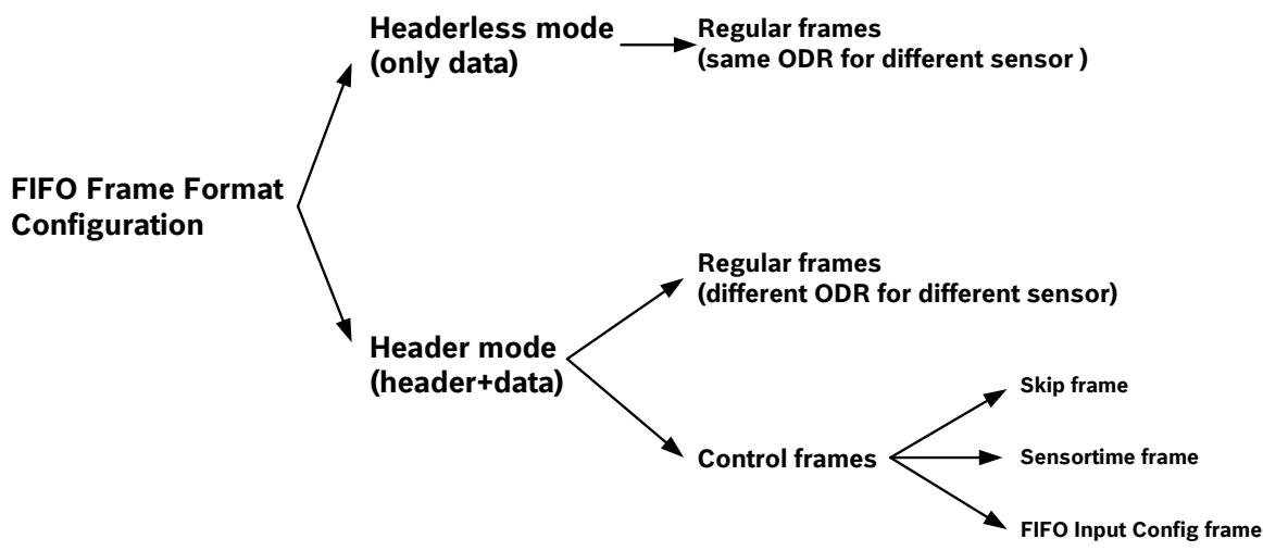
Figure 4: FIFO frame configurations
In headerless mode no header byte is used and the frames consist only of data bytes. The data bytes will always be sensor data. Only regular frames with the same ODR for all sensors are supported and no external interrupt flags are possible. This mode has the advantage of an easy frame format and an optimized usage of the 1024 bytes of FIFO storage. It can be selected by disabling fifo_header in Register (0x46-0x47) FIFO_CONFIG. In case of overreading the FIFO, non-valid frames always contain the fixed expression (magic number) 0x80 in the data frame.
In header mode every frame consists of a header byte followed by one or more data bytes. The header defines the frame type and contains parameters for the frame. The data bytes may be sensor data or control data. Header mode supports different ODRs for the different sensor data and external interrupt flags. This mode therefore has the advantage of allowing maximum flexibility of the FIFO engine. It is activated by enabling fifo_header in Register (0x46-0x47) FIFO_CONFIG.
2.5.1.3 Header byte format
The header format is shown below:
| Bit | 7 | 6 | 5 | 4 |
| Content | fh_mode<1:0> | fh_parm<3:2> | ||
| Bit | 3 | 2 | 1 | 0 |
| Read/Write | fh_parm<1:0> | fh_ext<1:0> | ||
| BOSCH | BMI160Data sheet | Page 25 | ||
The fh_mode, fh_opt and fh_ext fields are defined as
| fh_mode<1:0> | Definition | fh_parm <3:0> | fh_ext<1:0> |
| 0b10 | Regular | Frame content | Tag of INT2 and INT1 |
| 0b01 | Control | Control Opcode | |
| 0b00 | Reserved | Na | |
| 0b11 | Reserved | Na |
f_parm=0b0000 is invalid for regular mode, a header of 0x80 indicates an uninitialized frame.
2.5.1.4 Data bytes Format
When the FIFO is set to “headerless mode“, only sensor data will be saved into the FIFO (in the same order as in the data register). Any combination of accelerometer, gyroscope and external sensor data can be stored. External interrupt tags are not supported in headerless mode.
When the FIFO is set to “header mode“, the data byte format is different depending on the type of frame. There are two basic frame types, control frames and regular data frames. Each different type of control frame has its own data byte format. It can contain skipped frames, sensortime data or FIFO configuration information as explained in the following chapters. If the frame type is a regular frame (sensor data), the data byte section of the frame depend on how the data is being transmitted in this frame (as specified in the header byte section). It can include data from only one sensor or any combination of accelerometer, gyroscope and external sensor data.
2.5.1.5 Frame types
Regular frame (fh_mode=0b10)
Regular frames are the standard FIFO frames and contain sensor data. Regular frames can be identified by fh_mode set to 0b10 in the header byte section. The fh_parm frame defines which sensors are included in the data byte of the frame. The format of the fh_param is defined in the following table:
| Name | fh_parm<2:0> | |||
| Bit | 3 | 2 | 1 | 0 |
| Content | reserved | fifo_mag_data | fifo_gyr_data | fifo_acc_data |
When fifo_<sensor x>_data is set to ‘1’(‘0’), data for sensor x is included (not included) in the data part of the frame.
The fh_ext<1:0> field is set when an external interrupt is triggered. External interrupt tags are configured using int<x>_output_en in Register (0x53) INT_OUT_CTRL, int<x>_input_en in Register (0x54) INT_LATCH and fifo_tag_int<x>_en in Register (0x46-0x47) FIFO_CONFIG. For details, please refer to chapter 2.5.2.4.
The data byte part for regular data frames is identical to the format defined for the Register (0x04- 0x17) DATA. If a header indicates that not all sensors are included in the frame, these data are skipped and do not consume space in the FIFO.
Control frame (fh_mode=0b01):
Control frames, which are only available in header mode, are used for special or exceptional information. All control frames contribute to the fifo_byte _counter in Register (0x22-0x23) FIFO_LENGTH. In detail, there are three types of control frame, which can be distinguished by the fh_parm field:
Skip frame (fh_parm=0b000):
In case of a FIFO overflow, a skip frame is prepended to the FIFO content when the next readout is performed. A skip frame indicates the number of skipped frames since the last readout.
In the header byte of a FIFO_input_config frame, fh_mode equals 0b01 (since it is a control frame) and the fh_param equals 0b000 (indicating FIFO_input_config frame).
The data byte part of a skip frame consists of one byte and contains the number of skipped frames. When more than 0xFF frames have been skipped, 0xFF is returned.
Sensortime frame (fh_parm=0b001):
If the sensortime frame functionality is activated (see description of Register (0x46-0x47) FIFO_CONFIG) and the FIFO is overread, the last data frame is followed by a sensortime frame. This frame contains the BMI160 timestamp content corresponding th the time at which the last data frame was read.
In the header byte of a sensortime frame, fh_mode = 0b01 (since is a control frame) and fh_param = 0b001 (indicating sensortime frame). The data byte part of a sensortime frame consists of 3 bytes and contains the 24-bit sensortime. A sensortime frame does not consume memory in the FIFO.
FIFO_input_config frame (fh_parm=0b010):
Whenever the configuration of the FIFO input data sources changes, a FIFO input config frame is inserted into the FIFO in front of the data to which the configuration change is applied.
In the header byte of a FIFO_input_config frame, fh_mode = 0b01 (since it is a control frame) and fh_param = 0b010 (indicating FIFO_input_config frame). The data byte part of a FIFO_input_config Frame consists of one byte and contains data corresponding to the following table:
| Bit | 7 | 6 | 5 | 4 |
| Content | reserved | mag_if_ch | mag_conf_ch | |
| Bit | 3 | 2 | 1 | 0 |
| Read/Write | gyr_range_ch | gyr_conf_ch | acc_range_ch | acc_conf_ch |
gyr_range_ch: A change in Register (0x43) GYR_RANGE becomes active. gyr_conf_ch: A change in Register (0x42) GYR_CONF or gyr_fifo_filt_data or gyr_fifo_downsampling in Register (0x45) FIFO_DOWNS becomes active.
acc_range_ch: A change in Register (0x41) ACC_RANGE becomes active.
| BOSCH | BMI160Data sheet | Page 27 |
acc_conf_ch: A change in Register (0x40) ACC_CONF or acc_fifo_filt_data or acc_fifo_downsampling in Register (0x45) FIFO_DOWNS becomes active.
mag_if_ch: Will be set if there are changes on interface configuration (e.g. device address, read/write address). It can be used to switch to another device or different data-set within connected device.
mag_conf_ch: A change in Register (0x44) MAG_CONF becomes active.
2.5.2 FIFO conditions and details
2.5.2.1 Overflows
In the case of overflows the FIFO will overwrite the oldest data. A skip frame will be prepended at the next FIFO readout if the available FIFO space falls below the maximum size frame.
2.5.2.2 Overreads
If more data bytes are read from the FIFO than valid data bytes are available, ‘0x80’ is returned. Since a header ‘0x80’ indicates an invalid frame, the SW can recognize the end of valid data. After the invalid header the data is undefined. This is valid in both headerless and header mode. In addition, if header mode and the sensortime frame are enabled, the last data frame is followed by a sensortime frame. After this frame, a 0x80 header will be returned that indicates the end of valid data.
2.5.2.3 Partial frame reads
When a frame is only partially read through, it will be repeated within the next reading operation (including the header).
2.5.2.4 FIFO synchronization with external events
External events can be synchronized with the FIFO data by connecting the event source to one of the BMI160 interrupt pins (which needs to be configured as an input interrupt pin). External events can be generated e.g. by a camera module. Each frame contains the value of the interrupt input pin at the time of the external event.
The fh_ext<1:0> field is set when an external interrupt is triggered. External interrupt tags are configured using int<x>_output_en in Register (0x53) INT_OUT_CTRL, int<x>_input_en in Register (0x54) INT_LATCH and fifo_tag_int<x>_en in Register (0x46-0x47) FIFO_CONFIG.
2.5.2.5 FIFO Reset
A reset of the BMI160 is triggered by writing the opcode 0xB0 “fifo_flush“ to the Register (0x7E) CMD. This will clears all data in the FIFO while keeping the FIFO settings unchanged.
Automatic resets are only done in two exceptional cases where the data would not be usable without a reset:
a sensor is enabled or disabled in headerless mode,
a transition between headerless and headermode occurred.
| BOSCH | BMI160Data sheet | Page 28 |
2.5.2.6 Error Handling
In case of a configuration error in Register (0x46-0x47) FIFO_CONFIG, no data will be written into the FIFO and the error is reported in Register (0x02) ERR_REG.
2.6 Interrupt Controller
There are 2 interrupt output pins, to which thirteen different interrupt signals can be mapped independently via user programmable parameters.
Available interrupts supported by accelerometer in normal mode are:
Any-motion (slope) detection for motion detection
Significant motion
Step detector
Tap sensing for detection of single or double tapping events
Orientation detection
Flat detection for detection of a situation when one defined plane of the sensor is oriented parallel to the earth’s surface
Low-g/high-g for detecting very small acceleration (e.g. free-fall) or very high acceleration (e.g. shock events)
No/slow-motion detection for triggering an interrupt when no (or slow) motion occurs during a certain amount of time
In addition to that the common interrupts for accelerometer and gyroscope are
Data ready (“new-data”) for synchronizing sensor data read-out with the MCU / host controller
FIFO full / FIFO watermark allows FIFO fill level and overflow handling.
All Interrupts are available only in normal (low-noise) and low-power modes, but not in suspend mode. In suspend mode only the status (like orientation or flat) can be read out, but no interrupt will be triggered (unless latching is used).
If latching is used the interrupts (as well as the interrupt status) will be latched also in suspend mode, but no new interrupts will be generated.
Input Interrupt Pins: For special applications (e.g. PMU Trigger, FIFO Tag) interrupt pins can be configured as input pins. For all other cases (standard interrupts), the pin must be configured as an output.
Note: The direction of the interrupt pins is controlled with int<x>_output_en and int_x_input_en in Register (0x53) INT_OUT_CTRL and Register (0x54) INT_LATCH. If both are enabled, the input (e.g. marking fifo) is driven by the interrupt output.
2.6.1 Any-motion detection (Accel)
The any-motion detection uses the slope between two successive acceleration signals to detect changes in motion. The interrupt is configured in the Register (0x5F-0x62) INT_MOTION. It generates an interrupt when the absolute value of the acceleration exceeds a preset threshold int_anym_th for a certain number int_anym_dur of consecutive slope data points is above the slope threshold int_anym_th.
| BOSCH | BMI160Data sheet | Page 29 |
If the same number of data points falls below the threshold, the interrupt is reset. In order to avoid acceleration data saturation, when data is at maximal value (e.g. ‘0x8000’ or ‘0X7FFF’ for a 16 bit sensor); it is considered that the slope is at maximal value, too.

Figure 5: Any-motion (slope) interrupt detection
The criteria for any-motion detection are fulfilled and the slope interrupt is generated if any of the axis exceeds the threshold int_anym_th for int_anym_dur consecutive times. As soon as all the channels fall or stay below this threshold for int_anym_dur consecutive times the interrupt is reset. If this interrupt is triggered in latch mode it remains blocked (disabled) until the latching is cleared. The any-motion interrupt logic sends out the signals of the axis that has triggered the interrupt (int_anym_first_x, int_anym_first_y, int_anym_first_z) and the signal of motion direction (int_anym_sign).
2.6.2 Significant Motion (Accel)
The significant motion interrupt implements the interrupt required for motion detection in Android 4.3 and greater:
https://source.android.com/devices/sensors/composite\_sensors.html#Significant
A significant motion is a motion due to a change in the user location.
Examples of such significant motions are walking or biking, sitting in a moving car, coach or train, etc. Examples of situations that should not trigger significant motion include phone in pocket and person is not moving, phone is on a table and the table shakes a bit due to nearby traffic or washing machine.
| BOSCH | BMI160Data sheet | Page 30 |
The algorithm uses acceleration and performs the following steps to detect a significant motion:
Look for movement.
[Movement detected] Sleep for 3 seconds.
Look for movement. Either option a or option b will happen:
a. [One second has passed without movement] Go back to 1.
b. [Movement detected] Report that a significant movement has been found and wake up the application processor.
The significant motion and the anymotion interrupt are exclusive. To select the interrupt, use int_sig_mot_sel in Register (0x5F-0x62) INT_MOTION.
The following block diagram illustrates the algorithm:

Figure 6: Block diagram of significant motion interrupt algorithm
| BOSCH | BMI160Data sheet | Page 31 |
Configurable parameters are:
sig_th = 0x14; // ~ 70mg same as anym_th
t_skip = 0x01; // 2.56s 0=1.28s, 1=2.56s, 2=5,12s 3=10.24s
t_proof = 0x02; // 0.96s 0=0.24s, 1=0.48s, 2=0.96s 3=1.92s
2.6.3 Step Detector (Accel)
A step detection is the detection of a single step event, while the user is walking or running. The step detector is triggered when a peak is detected in the acceleration magnitude (vector length of 3D acceleration). In order to achieve a robust step detection the peak needs to exceed a configurable threshold min_threshold and a minimum delay time min_steptime between two consecutive peaks needs to be observed. The step detector can be configured in three modes:
Normal mode (default setting, recommended for most applications)
Sensitive mode (can be used for light weighted, small persons)
Robust mode (can be used, if many false positive detections are observed)
More details can be found in Register (0x7A-0x7B) STEP_CONF and the according step counter application note.
The step detector is the trigger for a step counter. The step counter is described in more detail in chapter 2.7.
2.6.4 Tap Sensing (Accel)
Double-Tap implements same functionality as two single taps in a short well-defined period of time. If the period of time is too short or too long no interrupt is fired.
The interrupt is configured in the Register (0x63-0x64) INT_TAP. When the preset threshold int_tap_th is exceeded, a tap is detected and a int_s_tap_int in Register (0x1C-0x1F) INT_STATUS is set and an interrupt is fired. The double-tap interrupt is generated only when a second tap is detected within a specified period of time. In this case, the int_d_tap_int in Register (0x1C-0x1F) INT_STATUS is set.
The slope between two successive acceleration data is needed to detect a tap-shock and quietperiod. The time difference between the two successive acceleration values depends on data rate selected for the interrupt source, which depends on the configured downsampling rate in Register (0x58-0x59) INT_DATA and the configured output data rate in Register (0x40) ACC_CONF, when filtered data have been selected in the Register (0x58-0x59) INT_DATA. The time delay int_tap_dur between two taps is typically between 12.5ms and 500ms. The threshold is typically between 0.7g and 1.5g in 2g measurement range. Due to different coupling between sensor and device shell (housing) and different measurement ranges of the sensor these parameters are configurable.
The criteria for a double-tap are fulfilled and an interrupt is generated if the second tap occurs after int_tap_quiet and within int_tap_dur. The tap direction is determined by the 1st tap. If during int_tap_quiet period (30/20ms) a tap occurs, it will be considered as a new tap.
The slope detection interrupt logic stores the direction of the (first) tap-shock in a status register. This register needs to be locked for int_tap_shock 50/75ms in order to prevent other slopes to overwrite this information.

Figure 7: Tap detection interrupt
The single-tap and double-tap interrupts are enabled through the int_s_tap_en and int_d_tap_en registers.
When a tap or double-tap interrupt is triggered, the signals of the axis that has triggered the interrupt (int_tap_first_x, int_tap_first_y, int_tap_first_z) and the signal of motion direction (int_tap_sign) will set in Register (0x1C-0x1F) INT_STATUS.
The axis on which the biggest slope occurs will trigger the tap. The second tap will be triggered by any axis (not necessarily same as the first tap).
If this interrupt is triggered in latch mode it remains blocked (disabled) until the latching is reset.
2.6.5 Orientation recognition (Accel)
The orientation recognition feature informs on an orientation change of the sensor with respect to the gravitational field vector g. There are the orientations face up/face down and orthogonal to that portrait upright, landscape left, portrait downside, and landscape right. The interrupt to face up/face down may be enabled separately through int_orient_ud_en in Register (0x65-0x66) INT_ORIENT.
The sensor orientation is defined by the angles phi and Theta (phi is rotation around the stationary z axis, theta is rotation around the stationary y axis).
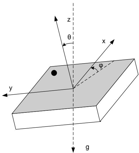
Figure 8: definition of coordinate system with respect to pin 1 marker
The measured acceleration vector components look as follows:
$$
a c c _ {x} = 1 g \cdot \sin \theta \cdot \cos \varphi\tag{1}
$$
$$
a c c _ {y} = - 1 g \cdot \sin \theta \cdot \sin \varphi\tag{2}
$$
$$
a c c _ {z} = 1 g \cdot \cos \theta\tag{3}
$$
$$
(2) / (1):
$$
$$
\frac {a c c _ {y}}{a c c _ {x}} = - \tan \varphi
$$
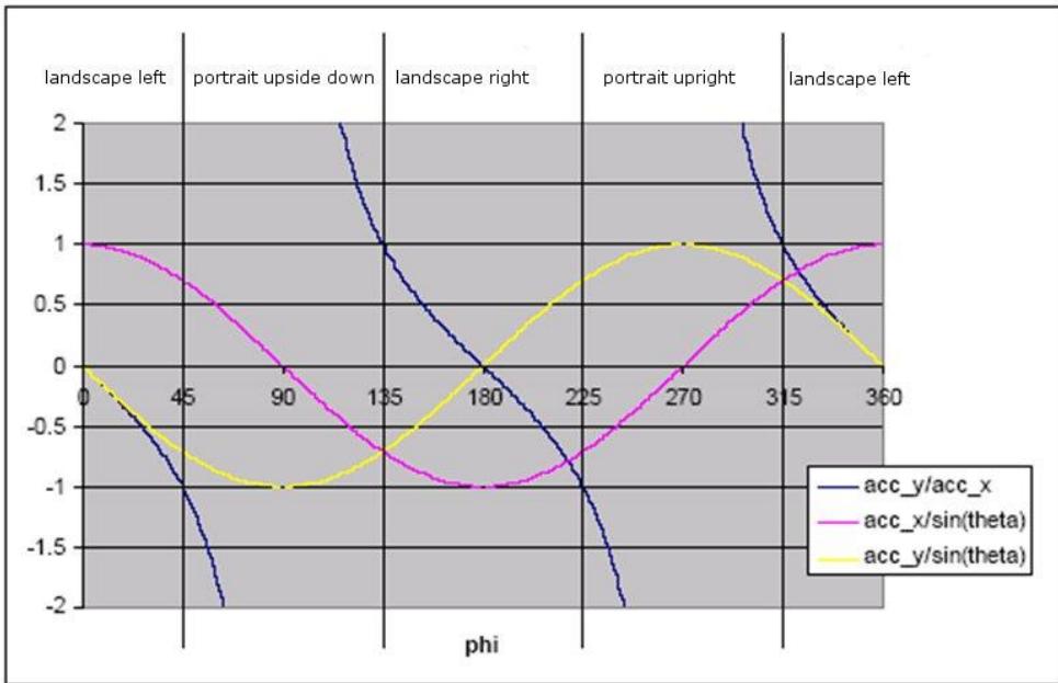
Figure 9: Angle-to-Orientation Mapping
| BOSCH | BMI160Data sheet | Page 34 |
Note that the sensor measures the direction of the force which needs to be applied to keep the sensor at rest (i.e. opposite direction than g itself).
Looking at the phone from frontside / portrait upright corresponds to the following angles:
$$
\theta = 9 0 ^ {\circ}, \varphi = 2 7 0 ^ {\circ}
$$
The orientation value is stored in the output register int_orient in Register (0x1C-0x1F) INT_STATUS. There are three orientation calculation modes: symmetrical, high-asymmetrical and low-asymmetrical. The mode is selected by the register int_orient_mode in Register (0x65- 0x66) INT_ORIENT as follows:
Table 14: Orientation mode
| orient_mode | Orientation mode |
| 00 | Symmetrical |
| 01 | High asymmetrical |
| 10 | Low asymmetrical |
| 11 | Symmetrical |
The register int_orient has the following meanings depending on the switching mode:
Table 15: Symmetrical mode
| orient | Name | Angle | Condition |
| x00 | landscape left | 315°<phi<45° | |acc_y/acc_x|<1 && acc_x≥0 |
| x01 | landscape right | 135°<phi<225° | |acc_y/acc_x|<1 && acc_x<0 |
| x10 | portrait upside down | 45°<phi<135° | |acc_y/acc_x|≥1 && acc_y<0 |
| x11 | portrait upright | 225°<phi<315° | |acc_y/acc_x|≥1 && acc_y≥0 |
Table 16: High asymmetrical mode
| orient | Name | Angle | Condition |
| x00 | landscape left | 297°<phi<63° | |acc_y/acc_x|<2 && acc_x≥0 |
| x01 | landscape right | 117°<phi<243° | |acc_y/acc_x|<2 && acc_x<0 |
| x10 | portrait upside down | 63°<phi<117° | |acc_y/acc_x|≥2 && acc_y<0 |
| x11 | portrait upright | 243°<phi<297° | |acc_y/acc_x|≥2 && acc_y≥0 |
Table 17: Low asymmetrical mode
| orient | Name | Angle | Condition |
| x00 | landscape left | 333°<phi<27° | |acc_y/acc_x|<0.5 && acc_x≥0 |
| x01 | landscape right | 153°<phi<207° | |acc_y/acc_x|<0.5 && acc_x<0 |
| x10 | portrait upside down | 27°<phi<153° | |acc_y/acc_x|≥0.5 && acc_y<0 |
| x11 | portrait upright | 207°<phi<333° | |acc_y/acc_x|≥0.5 && acc_y≥0 |
| BOSCH | BMI160Data sheet | Page 35 |
The engine uses 8 bits wide acceleration data for the orientation recognition. For upside or downside orientation, the int_orient<2> in Register (0x1C-0x1F) INT_STATUS has the definition
Table 18: upside and downside mode
| MSB acc_z | ||
| 0 upside | (270° < θ < 90°) | → acc_z >= 0 |
| 1 downside | (90° < θ < 270°) | → acc_z < 0 |
int_orient<2> also is computed when flat interrupt is activated.
Both portrait/landscape and upside/downside recognition use a hysteresis. The hysteresis for portrait/landscape detection is configurable and applies to all conditions as described in the tables below.
Table 19: Symmetrical mode
| orient | Name | Angle | Condition |
| x00 | landscape left | 315°+hy <phi< 45°-hy | |acc_y|<|acc_x|-hyst && acc_x≥0 |
| x01 | landscape right | 135°+hy <phi< 225°-hy | |acc_y|<|acc_x|-hyst && acc_x<0 |
| x10 | portrait upside down | 45°+hy <phi< 135°-hy | |acc_y|>|acc_x|hyst && acc_y<0 |
| x11 | portrait upright | 225°+hy <phi< 315°-hy | |acc_y|>|acc_x|hyst && acc_y≥0 |

Figure 10: Hysteresis in symmetrical mode
| BOSCH | BMI160Data sheet | Page 36 |
Table 20: High asymmetrical mode
| orient | Name | Angle | Condition |
| x00 | landscape left | 297°+hy <phi<63°-hy | |acc_y|<2*(|acc_x|-hyst) && acc_x≥0 |
| x01 | landscape right | 117°+hy <phi<243°-hy | |acc_y|<2*(|acc_x|-hyst) && acc_x<0 |
| x10 | portrait upside down | 63°+hy <phi<117°-hy | |acc_y|>2*|acc_x|+hyst && acc_y<0 |
| x11 | portrait upright | 243°+hy <phi<297°-hy | |acc_y|>2*|acc_x|+hyst && acc_y≥0 |

Figure 11: Hysteresis in high asymmetrical mode
Table 21: Low asymmetrical mode
| orient | Name | Angle | Condition |
| x00 | landscape left | 333°+hy <phi<27°-hy | |acc_y|<(|acc_x|-hyst)/2 && acc_x≥0 |
| x01 | landscape right | 153°+hy <phi<207°-hy | |acc_y|<(|acc_x|-hyst)/2 && acc_x<0 |
| x10 | portrait upside down | 27°+hy <phi<153°-hy | |acc_y|>|acc_x|/2+hyst && acc_y<0 |
| x11 | portrait upright | 207°+hy <phi<333°-hy | |acc_y|>|acc_x|/2+hyst && acc_y≥0 |

Figure 12: Hysteresis in low asymmetrical mode
| BOSCH | BMI160Data sheet | Page 37 |
The hysteresis for upside/downside detection is fixed to 11.5° which is ~200 mg (205 LSB in 2g mode and is scalable with the g range).
Table 22: Upside/downside hysteresis for all 3 modes
| orient | Name | Angle | Condition |
| 0xx | upside | 281.5°<Theta<78.5° | acc_z>200mg (|acc_z|>200mg and acc_z≥0) |
| 1xx | downside | 101.5°<phi<258° | acc_z<-200mg (|acc_z|>200mg and acc_z<0) |
2.6.5.1 Blocking
It is be possible to block the orientation detection (no orientation interrupt will be triggered). The orientation interrupt blocking feature is configurable via the int_orient_blocking in Register (0x65- 0x66) INT_ORIENT bits in the following manner:
“00” Interrupt blocking is disabled
“01” Interrupt blocked if device close to the horizontal position or acceleration of any axis >1.5g “10” Interrupt blocked if device close to the horizontal position or acceleration of any axis >1.5g or slope>0.2g (for 3 consecutive data samples)
“11” Interrupt blocked if device close to the horizontal position or slope>0.4g or acceleration of any axis>1.5g or another orientation change within 100ms (same orientation and acc <1.5g for 100ms)
For all states where interrupt blocking through slope detection is used, the interrupt is re-enabled after the slope has been below the threshold for 3 times in a row.
For all states where 100ms interrupt blocking is enabled, in order to trigger the interrupt, the orientation remains the same (stable) until the timer runs out (for ~100ms). The timer starts to count when orientation changes between two consecutive samples. If the orientation changes while timer is still counting, the timer is restarted.
The theta blocking (phone close to the horizontal position) is defined by the following inequality:
$$
\begin{array}{l} ((\text {theta_blk}) _ {6} * ((\text {acc_z}) _ {\text {SAT}} * (\text {acc_z}) _ {\text {SAT}}) _ {6}) _ {1 0} > ((\text {acc_x}) _ {\text {SAT}} * (\text {acc_x}) _ {\text {SAT}}) _ {1 0} + ((\text {acc_y}) _ {\text {SAT}} * \ (\text {acc_y}) _ {\text {SAT}}) _ {1 0} \end{array}
$$
where:
() means usage of 6-bit arithmetic (6 MSBs from a value is used);
() means absolute value reduced to 6 bits saturated to 1g (MSB-1 is taken as MSB, saturation arithmetic for this conversion)
If other than 2g range is selected, acceleration values shall be amplified before blocking computation to have the same scale as in 2g range.
2.6.5.2 Interrupt generation and latching
The orientation interrupt is triggered at every change of the int_orient status register value. If register bit int_orient_ud_en in Register (0x65-0x66) INT_ORIENT is ‘1’, then all bits in the int_orient register, those indicating the portrait/landscape orientation, as well as those indicating the upside/downside orientation are considered for the generation of the interrupt condition. If register bit int_orient_ud_en is ‘0’, then only the bits in the int_orient register that indicate the portrait/landscape orientation are considered for the generation of the interrupt condition, while those bits indicating the upside/downside orientation are ignored. The bit indicating upside/downside orientation is int_orient<2>, while the bit-field indicating the portrait/landscape orientation is int_orient<1:0>. If orient_ud_en is ‘0’ then the int_orient<2> status bit is 0.
In case the orientation interrupt condition has been satisfied the orientation relevant fields in Register (0x1C-0x1F) INT_STATUS are updated.
2.6.5.3 Rotation of the Reference Coordinate System
The given specification is valid for an upright mounted PCB. In order to also enable horizontal mounting, x and z axis can be exchanged via the register int_axes_ex for the flat and orientation interrupt. For all other interrupts and in all other functions, e.g. data registers and FIFO, the x, y, and z axes will not be affected. The x-, y-, z-axis will keep right-hand principle after the exchange
2.6.6 Flat Detection (Accel)
This interrupt detects flat orientation. This interrupt fires when the device gets into horizontal position (int_flat=1 e.g. it is being placed on a table) or when it goes out of it (int_flat=0 e.g. it is picked up).
The interrupt is configured in the Register (0x67-0x68) INT_FLAT. The condition for activating the interrupt is:
[((theta_flat) * ((acc_z) *(acc_z) ) ) – (“000000” & int_flat_hy) >= ((acc_x) *(acc_x) ) + ((acc_y) * (acc_y) ) AND (no_movement)
The condition to deactivate the interrupt in non-latched mode is:
[((theta_flat) * ((acc_z) *(acc_z) ) ) + (“000000” & int_flat_hy) < ((acc_x) *(acc_x) )10 + ((acc_y)SAT * (acc_y)SAT )10] OR NOT (no_movement)
no_movement is “0” if slope > 0.2g for 3 consecutive samples when orient_blocking = “10” no_movement is “0” if slope > 0.4g for 3 consecutive samples when orient_blocking = “11”
If no_movement is “1”, then flat interrupt is reset.

Figure 13: Flat Orientation Angles
| BOSCH | BMI160Data sheet | Page 39 |
Before the interrupt is actually fired, the device must remain flat for a certain period (e.g. int_flat_hold_time = 1s).
Note:
Rotation of the Reference Coordinate System is possible for the Flat interrupt, see chapter 2.6.5.3.
2.6.7 Low-g / free-fall Detection (Accel)
For freefall detection, the absolute values of the acceleration data of all axes are observed (global criteria). A sum of the absolute values of all accelerations |acc_x| + |acc_y| + |acc_z| is compared with the threshold int_low_th. The interrupt will be generated if the threshold is exceeded and the measured acceleration stays below the hysteresis level int_low_th+int_low_hy for some minimum number of samples (int_low_dur).

Figure 14: Free-fall detection
2.6.8 High-g detection (Accel)
This interrupt is configured in the Register (0x5A-0x5E) INT_LOWHIGH. The interrupt is asserted if the absolute value of acceleration data of at least one enabled axis exceeds the programmed threshold int_high_th and the sign of the value does not change for a minimum duration of int_high_dur. The interrupt condition is cleared when the absolute value of acceleration data of all selected axes falls below the threshold int_high_th minus the hysteresis int_high_hy or if the sign of the acceleration value changes. The X, Y and Z axes are enabled with the int_high_en_x, int_high_en_y, and int_high_en_z, respectively.
| BOSCH | BMI160Data sheet | Page 40 |
When the high-g interrupt is triggered, the signals of the axis that has triggered the interrupt (int_high_first_x, int_high_first_y, int_high_first_z) and the motion direction (int_high_sign) are set in the Register (0x1C-0x1F) INT_STATUS.
If this interrupt is triggered in latch mode it stays blocked (disabled) until the latching is cleared.
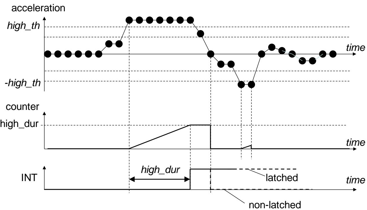
Figure 15: Free-fall detection
2.6.9 Slow-Motion Alert / No-Motion Interrupt (Accel)
This interrupt engine monitors the slopes of each axis. The interrupt is configured in the Register (0x5F-0x62) INT_MOTION. It behaves similar to the any-motion interrupt, but with a different set of the parameters. As the only difference between the slow-motion interrupt and the any-motion interrupt, the slow-motion engine doesn’t store the information which axis has triggered the interrupt and in which direction.
The slow-motion/no-motion interrupt engine can be configured in two modes. It can act as an interrupt very similar to the any-motion interrupt, where the slope on the selected axis is monitored and an interrupt is generated when a slope threshold is exceeded for a programmable number of samples. The figure below illustrates the operation of the slow-motion interrupt engine in terms of relevant signals and timing.
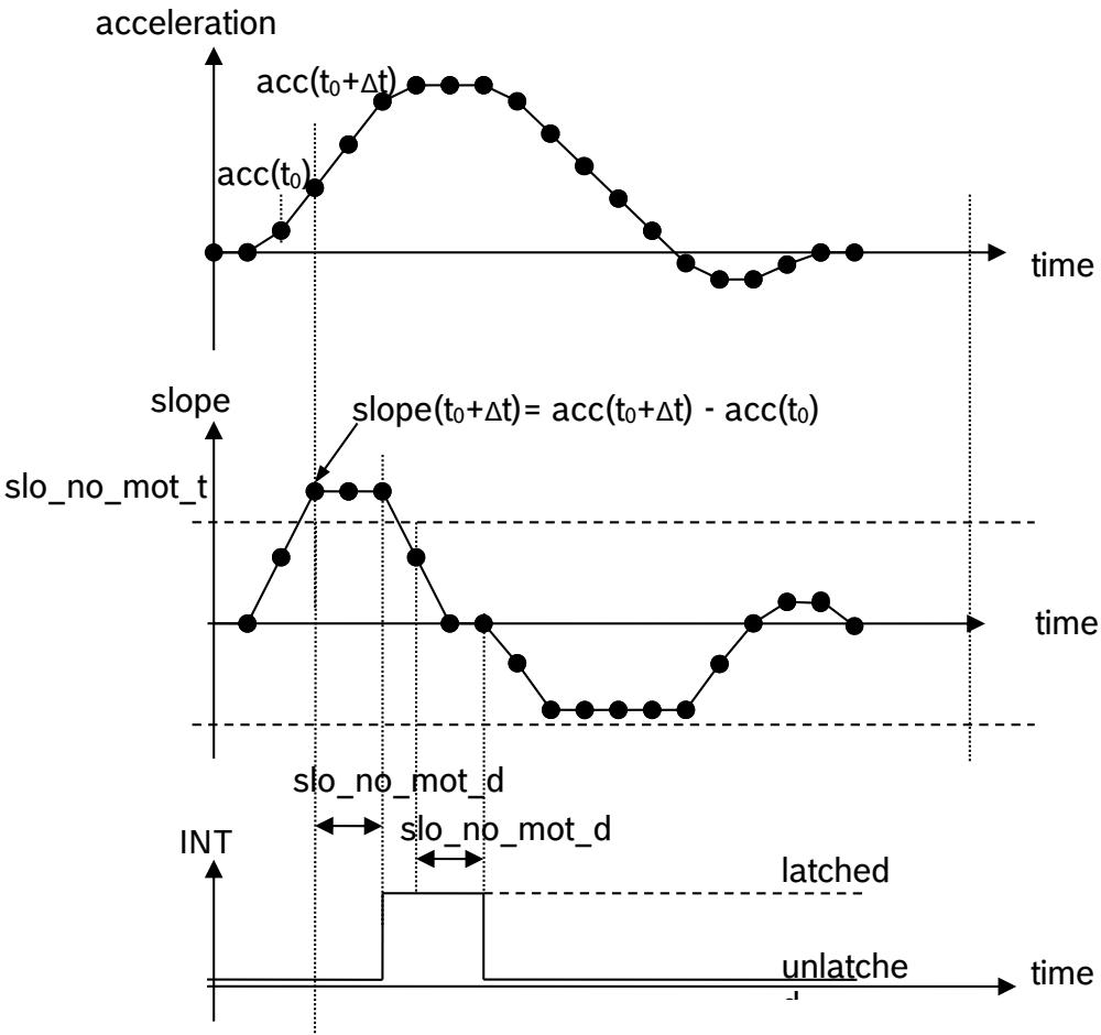
Figure 16: Slow motion, no motion
The interrupt engine can also be configured as a no-motion interrupt, where an interrupt is generated when the slope on all selected axis remains smaller than a programmable threshold for a programmable time. In order to save register space, some configuration registers have different interpretations depending on the selected mode. The signals and timings relevant to the no-motion interrupt functionality are depicted in the figure below.

Figure 17: Signal timings no motion interrupt
The figure below shows the differences in the logic operation between the slow-motion and nomotion interrupt functionality.

Figure 18: Slow motion interrupt modeslo_no_mot_du

Figure 19: No motion interrupt mode
| BOSCH | BMI160Data sheet | Page 43 |
2.6.9.1 Register slo_no_mot_dur
The meaning of register int_slo_no_mot_dur changes depending on the state of the no_mot_sel configuration bit. If int_no_mot_sel =’0’, register int_slo_no_mot_dur defines the number of consecutive slope data points of the selected axis which must exceed the threshold value int_slo_no_mot_th for an interrupt to be asserted. Register (0x5F-0x62) INT_MOTION lists the relationship between the setting of int_slo_no_mot_dur and the number of slope data points filtered prior to asserting the interrupt.
However, if no_mot_sel =’1’, register int_slo_no_mot_dur defines the time no slope data point of any of the selected axis must exceed the threshold value int_slo_no_mot_th for an interrupt to be asserted. The tick times of 1.28s, 5.12s and 10.24s depend on the value programmed into int_slo_no_mot_dur<5:0>. By means of using variable tick times, a no-motion delay between 1s and 430s may be adjusted.
2.6.9.2 Register slo_no_mot_th
The int_slo_no_mot_th register defines the threshold against which the calculated slope values of each axis are compared. The scaling is independent on the selected interrupt mode. The user must scale the int_slo_no_mot_th value according to the adjusted range.
2.6.10 Data Ready Detection (Accel, Gyro and external sensors)
This interrupt fires whenever a new data sample from accel and gyro is complete. This allows a low latency data readout.
The data update detection monitors the data_update signals for all axes and sensors. It generates an interrupt as soon as the values for all axes and sensors which are required for the configured output data rates have been updated.
The interrupt is cleared automatically when the update for the next sample starts or the data is read out from the data register.
2.6.11 PMU Trigger (Gyro)
Whenever a PMU (power management unit) trigger (either wakeup or sleep) is issued, wakeup_int in Register (0x6C) PMU_TRIGGER configures if an interrupt is send to the application processor. If the AP wants to trigger sleeps itself for the gyro, the gyr_wakeup_trigger is configured accordingly and no wakeup triggers are issued.
The PMU trigger interrupt is from the system perspective used in a similar manner as the anymotion and nomotion interrupts. The PMU trigger interrupt follows the Register (0x54) INT_LATCH configuration for resetting the interrupt.
2.6.12 FIFO Interrupts (Accel, Gyro, and external sensors)
The FIFO supports two interrupts, a FIFO full interrupt and a watermark interrupt. The FIFO full interrupt is issued when the FIFO is full and the next full data sample would cause a FIFO overflow, which may lead to samples being deleted. Technically, that means that a FIFO full interrupt is issued, whenever less space than two maximum size frames is left in the FIFO. The FIFO watermark interrupt is fired, when the FIFO fill level in fifo_byte_counter in Register (0x22- 0x23) FIFO_LENGTH is above a pre-configured watermark, defined in fifo_watermark in Register (0x46-0x47) FIFO_CONFIG.
Note: The unit of fifo_watermark is 4 bytes whereas the unit of fifo_byte_counter is single bytes.
| BOSCH | BMI160Data sheet | Page 44 |
2.7 Step Counter
The step counter implements the function required for step counting in Android 4.4 and greater: https://source.android.com/devices/sensors/sensor-types#step\_counter
The step counter accumulates the steps detected by the step detector interrupt. Based on more sophisticated algorithms, the step counter features a higher accuracy and reporting latency than the step detector interrupt described in Chapter 2.6.3.
The step counter is configurable to the following modes through the step detector settings:
Normal mode (default setting, recommended for most applications)
Sensitive mode (can be used for light weighted, small persons)
Robust mode (can be used, if many false positive detections are observed)
In order to read out the step counter values it is recommended to switch to normal mode
The step counter is enabled and reset with step_cnt_en in Register (0x7A-0x7B) STEP_CONF. It shares its configuration with the step detector interrupt in Register (0x7A-0x7B) STEP_CONF.
The step counter can be used in low-power mode. In order to receive the most recent number of counted steps, it is recommended to switch to normal mode prior to reading out the Registe (0x78-0x79) STEP_CNT.
More details can be found in the step counter field test report.
2.8 Device self test
This feature permits to check the sensor functionality via a built-in self-test (BIST). The accelerometer has a comprehensive self test function for the MEMS element, the gyroscope implements a simple self-test/life-test.
2.8.1 Self-test accelerometer
By applying electrostatic forces to the sensor core instead of external accelerations, the entire signal path of the sensor can be tested. Activating the self-test results in a static offset of the acceleration data; any external acceleration or gravitational force applied to the sensor during active self-test will be observed in the output as a superposition of both acceleration and self-test signal. All three axes are activated at the same time.
Before the self-test is enabled the g-range should be set to 8 g. The Register (0x40) ACC_CONF has to be set to value 0x2C (acc_odr=1600Hz; acc_bwp=2; acc_us=0). Otherwise the accelerometer self-test mode will not function correctly.
The self-test is activated by writing the value ´0b01´ to the acc_self_test_enable bits in the Register (0x6D) SELF_TEST. It is possible to control the direction of the deflection of all 3 axes through the bit acc_self_test_sign. The excitations occurs in negative (positive) direction if self_test_sign = ´0b0´ (´0b1´). The amplitude of the deflection has to be set high by writing acc_self_test_amp=´0b1´. After the self-test is enabled, the user should wait 50 ms before interpreting the acceleration data
| BOSCH | BMI160Data sheet | Page 45 |
In order to ensure a proper interpretation of the self-test signal it is recommended to perform the self-test for both (positive and negative) directions and then to calculate the difference of the resulting acceleration values. The table below shows the minimum absolute differences for each axis. The actually measured absolute signal differences can be significantly larger.
Table 23: Accelerometer self test minimum difference values
| x-axis signal | y-axis signal | z-axis signal | |
| Minimum difference signal | 2 g | 2 g | 2 g |
It is recommended to perform a reset of the device after a self-test has been performed. If the reset cannot be performed, the following sequence must be kept to prevent unwanted interrupt generation: disable interrupts, change parameters of interrupts, wait for at least 50ms, enable desired interrupts.
2.8.2 Self-test gyroscope
The gyroscope BIST can be triggered during normal operation mode. It checks the sensors drive amplitude, its frequency and the stability of the drive control loop. Hence, disturbances of the movement by particles, mechanical damage or pressure loss can be detected.
The self-test for the gyroscope will be started by writing a ‘1’ to gyr_self_test_enable in Register (0x6D) SELF_TEST. The result will be in gyr_self_test_ok in Register (0x1B) STATUS.
In addition, any particles or damages can be easily identified in a „Manual Performance Check“. Due to the outstanding offset and noise performance the measured values at zero-rate fit the specified performance.
2.9 Offset Compensation
BMI160 offers fast and manual compensation as well as inline calibration.
Fast offset compensation is performed with pre-filtered data, and the offset is then applied to both, pre-filtered and filtered data. If necessary the result of this computation is saturated to prevent any overflow errors (the smallest or biggest possible value is set, depending on the sign). The public offset compensation Register (0x71-0x77) OFFSET are images of the corresponding registers in the NVM. With each image update (see chapter 2.10 for details) the contents of the NVM registers are written to the public registers. The public registers can be overwritten by the user at any time. Offset compensation needs to be enabled through gyr_off_en and acc_off_en in Register (0x71-0x77) OFFSET.
2.9.1 Fast offset compensation
Fast offset compensation (FOC) is a one-shot process that compensates offset errors of accelerometer and gyro by setting the offset compensation registers to the negated offset error. This is best suited for “end-of-line trimming” with the customers device positioned in a well-defined orientation.
Before triggering, the FOC needs to be configured via the Register (0x69) FOC_CONF. Accelerometer and gyroscope FOC can be separately disabled or enabled. Gyroscope target value is always 0 dps, for the accelerometer the target value has to be defined for each channel (-1g, 0g, +1g) depending on sensor position relative to the earth gravity field.
| BOSCH | BMI160Data sheet | Page 46 |
FOC is triggered by issuing a start_foc command to Register (0x7E) CMD. Once triggered, the status of the fast correction process is reflected in the status bit foc_rdy in Register (0x1B) STATUS. Foc_rdy is ‘0’ while the measurement is in progress. Accelerometer and gyroscope values are measured with preset filter settings. This will take a maximum time of 250 ms.
The negated measured values are written to Register (0x71-0x77) OFFSET automatically (overwriting previous offset register values), cancelling out offset errors if “gyr_off_en” and “acc_off_en” in Register (0x71-0x77) OFFSET are activated.
For the accelerometer offset, the accuracy is 3.9 mg.
Fast compensation should not be used in combination with the low-power mode. In low-power mode the conditions (availability of necessary data) for proper function of fast compensation are not fulfilled.
Fast offset compensation does not clear the data ready bit in Fast offset compensation does not clear the data ready bit in
Register (0x1B) STATUS. It is recommended to read the Register (0x04-0x17) DATA after FOC completes, to remove a stall data ready bit from before the FOC.
2.9.2 Manual offset compensation
The contents of the public compensation Register (0x71-0x77) OFFSET may be set manually via the digital interface. After modifying the Register (0x71-0x77) OFFSET the next data sample is not valid.
Writing to the offset compensation registers is not allowed while the fast compensation procedure is running.
“gyr_off_en” and “acc_off_en” in Register (0x71-0x77) OFFSET need to be activated as well.
2.9.3 Inline calibration
For certain applications, it is often desirable to calibrate the offset once and to store the compensation values permanently. This can be achieved by using fast or manual offset compensation to determine the proper compensation values and then storing these values permanently in the NVM.
Each time the device is reset, the compensation values are loaded from the non-volatile memory into the image registers and used for offset compensation.
2.10 Non-Volatile Memory
The entire memory of the BMI160 consists of volatile and non-volatile registers. Part of it can be both read and written by the user. Access to non-volatile memory is only possible through (volatile) image registers.
We support a maximum number of write cycles equal or less than 14.
| BOSCH | BMI160Data sheet | Page 47 |
The Register (0x70) NV_CONF and Register (0x71-0x77) OFFSET have an NVM backup which is accessible by the user.
The content of the NVM is loaded to the image registers after a reset (either POR or softreset). As long as the image update is in progress, bit nvm_rdy in Register (0x1B) STATUS is ´0´, otherwise it is ´1´.
The image registers can be read and written like any other register.
Writing to the NVM is a three-step procedure:
Write the new contents to the image registers.
Write ´1´ to bit nvm_prog_en in the Register (0x6A) CONF register in order to unlock the NVM. Write prog_nvm (0xA0) to the Register (0x7E) CMD to trigger the write process.
Writing to the NVM always renews the entire NVM contents. It is possible to check the write status by reading bit nvm_rdy. While nvm_rdy = ´0´, the write process is still in progress; if nvm_rdy = ´1´, then writing is completed. As long as the write process is ongoing, no change of power mode and image registers is allowed. An NVM write cycle can only be initiated, when the accelerometer is in normal mode.
2.11 Register Map
This chapter contains register definitions. REG[x]<y> denotes bit y in byte x in register REG. Val(Name) is the value contained in the register interpreted as non-negative binary number. When writing to reserved bits, ‘0’ should be written when not stated different.
| Read/write | read only | write only | reserved | ||||||||
| Register Address | Register Name | Default Value | bit7 | bit6 | bit5 | bit4 | bit3 | bit2 | bit1 | bit0 | |
| 0x7E | CMD | 0x00 | cmd | ||||||||
| 0x7D | - | - | reserved | ||||||||
| 0x7C | - | - | reserved | ||||||||
| 0x7B | STEP_CONF_1 | 0x03 | reserved | step_cnt_en | step_conf_10_8 | ||||||
| 0x7A | STEP_CONF_0 | 0x15 | step_conf_7_0 | ||||||||
| 0x79 | STEP_CNT_1 | 0x00 | step_cnt_15_8 | ||||||||
| 0x78 | STEP_CNT_0 | 0x00 | step_cnt_7_0 | ||||||||
| 0x77 | OFFSET_6 | 0x00 | gyr_off_en | acc_off_en | off_gyr_z_9_8 | off_gyr_y_9_8 | off_gyr_x_9_8 | ||||
| 0x76 | OFFSET_5 | 0x00 | off_gyr_z_7_0 | ||||||||
| 0x75 | OFFSET_4 | 0x00 | off_gyr_y_7_0 | ||||||||
| 0x74 | OFFSET_3 | 0x00 | off_gyr_x_7_0 | ||||||||
| 0x73 | OFFSET_2 | 0x00 | off_acc_z | ||||||||
| 0x72 | OFFSET_1 | 0x00 | off_acc_y | ||||||||
| 0x71 | OFFSET_0 | 0x00 | off_acc_x | ||||||||
| 0x70 | NV_CONF | 0x00 | reserved | u_spare_0 | i2c_wdt_en | i2c_wdt_sel | spi_en | ||||
| 0x6F | - | - | reserved | ||||||||
| 0x6E | - | - | reserved | ||||||||
| 0x6D | SELF_TEST | 0x00 | reserved | gyr_self_test_enable | acc_self_test_amp | acc_self_test_sign | acc_self_test_enable | ||||
| 0x6C | PMU_TRIGGER | 0x00 | reserved | wakeup_int | gyr_sleep_state | gyr_wakeup_trigger | gyr_sleep_trigger | ||||
| 0x6B | IF_CONF | 0x00 | reserved | if_mode | reserved | spi3 | |||||
| 0x6A | CONF | 0x00 | reserved | nvm_prog_en | reserved | ||||||
| 0x69 | FOC_CONF | 0x00 | reserved | foc_gyr_en | foc_acc_x | foc_acc_y | foc_acc_z | ||||
| 0x68 | INT_FLAT_1 | 0x11 | reserved | int_flat_hold | reserved | int_flat_hy | |||||
| 0x67 | INT_FLAT_0 | 0x08 | reserved | int_flat_theta | |||||||
| 0x66 | INT_ORIENTATION_1 | 0x48 | int_orient_axes_ex | int_orient_ud_en | int_orient_theta | ||||||
| 0x65 | INT_ORIENTATION_0 | 0x18 | int_orient_hy | int_orient_blocking | int_orient_mode | ||||||
| 0x64 | INT_TAP_1 | 0x0A | reserved | int_tap_th | |||||||
| 0x63 | INT_TAP_0 | 0x04 | int_tap_quiet | int_tap_shock | reserved | int_tap_dur | |||||
| 0x62 | INT_MOTION_3 | 0x24 | reserved | int_sig_mot_proof | int_sig_mot_skip | int_sig_mot_sel | int_slo_nomo_sel | ||||
| 0x61 | INT_MOTION_2 | 0x14 | int_slo_nomo_th | ||||||||
| 0x60 | INT_MOTION_1 | 0x14 | int_anymo_th | ||||||||
| 0x5F | INT_MOTION_0 | 0x00 | int_slo_nomo_dur | int_anym_dur | |||||||
| 0x5E | INT_LOWHIGH_4 | 0xC0 | int_high_th | ||||||||
| 0x5D | INT_LOWHIGH_3 | 0x0B | int_high_dur | ||||||||
| 0x5C | INT_LOWHIGH_2 | 0x81 | int_high_hy | reserved | int_low_hy | ||||||
| 0x5B | INT_LOWHIGH_1 | 0x30 | int_low_th | ||||||||
| 0x5A | INT_LOWHIGH_0 | 0x07 | int_low_dur | ||||||||
| 0x59 | INT_DATA_1 | 0x00 | int_motion_src | reserved | |||||||
| 0x58 | INT_DATA_0 | 0x00 | int_low_high_src | reserved | int_tap_src | reserved | |||||
| 0x57 | INT_MAP_2 | 0x00 | int2_flat | int2_orient | int2_s_tap | int2_d_tap | int2_nomotion | int2_anymotion | int2_highg | int2_lowg_step | |
| 0x56 | INT_MAP_1 | 0x00 | int1_drdy | int1_fwm | int1_ffull | int1_pmu_trig | int2_drdy | int2_fwm | int2_ffull | int2_pmu_trig | |
| 0x55 | INT_MAP_0 | 0x00 | int1_flat | int1_orient | int1_s_tap | int1_d_tap | int1_nomotion | int1_anymotion | int1_highg | int1_lowg_step | |
| 0x54 | INT_LATCH | 0x00 | reserved | int2_input_en | int1_input_en | int_latch | |||||
| 0x53 | INT_OUT_CTRL | 0x00 | int2_output_en | int2_od | int2_lvll | int2_edge_ctrl | int1_output_en | int1_od | int1_lvll | int1_edge_ctrl | |
| 0x52 | INT_EN_2 | 0x00 | reserved | int_step_det_en | int_nomoz_en | int_nomoy_en | int_nomox_en | ||||
| 0x51 | INT_EN_1 | 0x00 | reserved | int_fwm_en | int_ffull_en | int_drdy_en | int_low_en | int_highg_z_en | int_highg_y_en | int_highg_x_en | |
| 0x50 | INT_EN_0 | 0x00 | int_flat_en | int_orient_en | int_s_tap_en | int_d_tap_en | reserved | int_anymo_z_en | int_anymo_y_en | int_anymo_x_en | |
| 0x4F | MAG_IF_4 | 0x00 | write_data | ||||||||
| 0x4E | MAG_IF_3 | 0x4C | write_addr | ||||||||
| 0x4D | MAG_IF_2 | 0x42 | read_addr | ||||||||
| 0x4C | MAG_IF_1 | 0x80 | mag_manual_en | reserved | mag_offset | mag_rd_burst | |||||
| 0x4B | MAG_IF_0 | 0x20 | i2c_device_addr | reserved | |||||||
| 0x4A | - | - | reserved | ||||||||
| 0x48 | - | - | reserved | ||||||||
| 0x47 | FIFO_CONFIG_1 | 0x10 | fifo_gyr_en | fifo_acc_en | fifo_mag_en | fifo_header_en | fifo_tag_int1_en | fifo_tag_int2_en | fifo_time_en | reserved | |
| 0x46 | FIFO_CONFIG_0 | 0x80 | fifo_water_mark | ||||||||
| 0x45 | FIFO_DOWN | 0x88 | acc_fifo_filt_data | acc_fifo_downs | gyr_fifo_filt_data | gyr_fifo_downs | |||||
| 0x44 | MAG_CONF | 0x0B | reserved | mag_odr | |||||||
| 0x43 | GYR_RANGE | 0x00 | reserved | gyr_range | |||||||
| 0x42 | GYR_CONF | 0x28 | reserved | gyr_bwp | gyr_odr | ||||||
| 0x41 | ACC_RANGE | 0x03 | reserved | acc_range | |||||||
Bosch Sensortec
| 0x40 | ACC_CONF | 0x28 | acc_us | acc_bwp | acc_odr | |||||
| 0x3F | - | - | reserved | |||||||
| 0x25 | - | - | reserved | |||||||
| 0x24 | FIFO_DATA | 0x00 | fifo_data | |||||||
| 0x23 | FIFO_LENGTH_1 | 0x00 | reserved | fifo_byte_counter_10_8 | ||||||
| 0x22 | FIFO_LENGTH_0 | 0x00 | fifo_byte_counter_7_0 | |||||||
| 0x21 | TEMPERATURE_1 | 0x80 | temperature_15_8 | |||||||
| 0x20 | TEMPERATURE_0 | 0x00 | temperature_7_0 | |||||||
| 0x1F | INT_STATUS_3 | 0x00 | flat | orient_2 | orient_1_0 | high_sign | high_first_z | high_first_y | high_first_x | |
| 0x1E | INT_STATUS_2 | 0x00 | tap_sign | tap_first_z | tap_first_y | tap_first_x | anym_sign | anym_first_z | anym_first_y | anym_first_x |
| 0x1D | INT_STATUS_1 | 0x00 | nomo_int | fwm_int | ffull_int | drdy_int | lowg_int | highg_int | reserved | |
| 0x1C | INT_STATUS_0 | 0x00 | flat_int | orient_int | s_tap_int | d_tap_int | pmu_trigger_int | anym_int | sigmot_int | step_int |
| 0x1B | STATUS | 0x01 | drdy_acc | drdy_gyr | drdy_mag | nvm_rdy | foc_rdy | mag_man_op | gyr_self_test_ok | reserved |
| 0x1A | SENSORTIME_2 | 0x00 | sensor_time_23_16 | |||||||
| 0x19 | SENSORTIME_1 | 0x00 | sensor_time_15_8 | |||||||
| 0x18 | SENSORTIME_0 | 0x00 | sensor_time_7_0 | |||||||
| 0x17 | DATA_19 | 0x00 | acc_z_15_8 | |||||||
| 0x16 | DATA_18 | 0x00 | acc_z_7_0 | |||||||
| 0x15 | DATA_17 | 0x00 | acc_y_15_8 | |||||||
| 0x14 | DATA_16 | 0x00 | acc_y_7_0 | |||||||
| 0x13 | DATA_15 | 0x00 | acc_x_15_8 | |||||||
| 0x12 | DATA_14 | 0x00 | acc_x_7_0 | |||||||
| 0x11 | DATA_13 | 0x00 | gyr_z_15_8 | |||||||
| 0x10 | DATA_12 | 0x00 | gyr_z_7_0 | |||||||
| 0x0F | DATA_11 | 0x00 | gyr_y_15_8 | |||||||
| 0x0E | DATA_10 | 0x00 | gyr_y_7_0 | |||||||
| 0x0D | DATA_9 | 0x00 | gyr_x_15_8 | |||||||
| 0x0C | DATA_8 | 0x00 | gyr_x_7_0 | |||||||
| 0x0B | DATA_7 | 0x00 | rhall_15_8 | |||||||
| 0x0A | DATA_6 | 0x00 | rhall_7_0 | |||||||
| 0x09 | DATA_5 | 0x00 | mag_z_15_8 | |||||||
| 0x08 | DATA_4 | 0x00 | mag_z_7_0 | |||||||
| 0x07 | DATA_3 | 0x00 | mag_y_15_8 | |||||||
| 0x06 | DATA_2 | 0x00 | mag_y_7_0 | |||||||
| 0x05 | DATA_1 | 0x00 | mag_x_15_8 | |||||||
| 0x04 | DATA_0 | 0x00 | mag_x_7_0 | |||||||
| 0x03 | PMU_STATUS | 0x00 | reserved | acc_pmu_status | gyr_pmu_status | mag_pmu_status | ||||
| 0x02 | ERR_REG | 0x00 | mag_drdy_err | drop_cmd_err | i2c_fail_err | err_code | fatal_err | |||
| 0x01 | - | - | reserved | |||||||
| 0x00 | CHIP_ID | 0xD1 | chip_id | |||||||
Figure 20: BMI160 register map
| BOSCH | BMI160Data sheet | Page 50 |
2.11.1 Register (0x00) CHIPID
ADDRESS 0x00
RESET na
MODE R
DESCRIPTION The register contains the chip identification code. DEFINITION
| Name | Register (0x00) CHIPID | |||
| Bit | 7 | 6 | 5 | 4 |
| Read/Write | R | R | R | R |
| Reset Value | 1 | 1 | 0 | 1 |
| Content | chip_id<7:4> | |||
| Bit | 3 | 2 | 1 | 0 |
| Read/Write | R | R | R | R |
| Reset Value | 0 | 0 | 0 | 1 |
| Content | chip_id<3:0> | |||
2.11.2 Register (0x02) ERR_REG
ADDRESS 0x02
RESET 0b00000000
MODE RW
DESCRIPTION Reports sensor error flags. Flags are reset when read.
DEFINITION
| Bit | Acronym | Definition |
| 7 | Reserved | |
| 6 | drop_cmd_err | Dropped command to Register |
| 5 | Reserved | |
| 4:1 | error_code | 0000: no error0001: error0010: error0011: low-power mode and interrupt uses pre-filtered data0100: reserved0101: reserved0110: ODRs of enabled sensors in header-less mode do not match0111: pre-filtered data are used in low power mode1000-1111: reservedThe first reported error will be shown in the error code. |
| 0 | fatal_err | Chip not operable |
| BOSCH | BMI160Data sheet | Page 51 |
The register is meant for debug purposes, not for regular verification if an operation completed successfully.
Extensions under consideration:
fatal_err: Error during bootup. Broken hardware (e.g. NVM error, see ASIC spec for details). This flag will not be cleared after reading the register. The only way to clear the flag is a POR.
Acc_conf_err: Accelerometer ODR and BW not compatible
gyr_conf_err: Gyroscope ODR and BW not compatible
Error flags (bits 7:4) store error event until they are reset by reading the register.
2.11.3 Register (0x03) PMU_STATUS
ADDRESS 0x03 RESET 0b0000-0000 MODE R DESCRIPTION Shows the current power mode of the sensor. DEFINITION
| Name | Register (0x03) PMU_STATUS | |||
| Bit | 7 | 6 | 5 | 4 |
| Read/Write | R | R | R | R |
| Reset Value | 1 | 0 | 0 | 0 |
| Content | reserved | acc_pmu_status | ||
| Bit | 3 | 2 | 1 | 0 |
| Read/Write | R | R | R | R |
| Reset Value | 0 | 0 | 0 | 0 |
| Content | gyr_pmu_status | mag_pmu_status | ||
| acc_pmu_status | Accel Mode |
| 0b00 | Suspend |
| 0b01 | Normal |
| 0b10 | Low Power |
| gyr_pmu_status | Gyro Mode |
| 0b00 | Suspend |
| 0b01 | Normal |
| 0b10 | Reserved |
| 0b11 | Fast Start-Up |
| mag_pmu_status | Magnet Mode |
| 0b00 | Suspend |
| 0b01 | Normal |
| 0b10 | Low Power |
| BOSCH | BMI160Data sheet | Page 52 |
The register reflects the current power modes of all sensor configured as soon as they are effective. If a sensor is enabled, the new sensor mode is reported as soon as the MEMS is up and before digital filters have settled. The settling time depends on filter settings. The power modes may be changed through the Register (0x7E) CMD. In addition, for the gyroscope through register events may be defined, which change the gyro power mode.
In low power mode the FIFO is not accessible. For read outs of the FIFO the sensor has to be set to normal mode, after read-out the sensor can be set back to low power mode.
2.11.4 Register (0x04-0x17) DATA
ADDRESS 0x04 (20 byte)
RESET (BYTEWISE) 0b0000-0000
MODE R
DESCRIPTION Register for accelerometer, gyroscope and magnetometer data. DATA[0-19] are treated as atomic update unit with respect to an I2C/SPI operation. A read operation on the Register (0x04-0x17) DATA resets the appropriate *_drdy bits in
Register (0x1B) STATUS. E.g. when only 0 is read, only drdy_gyr is reset. DEFINITION
DATA[0-19] contains the latest data for the x, y, and z axis of magnetometer MAG_[X-Z], gyroscope GYR_[X-Z], and accelerometer ACC_[X-Z]. The rationale for the ordering is the probability for these configurations is decreasing
Readout of accel and sensortime
Readout of gyro, accel, and sensortime
Readout of magnetometer, gyro, accel, and sensortime
Readout of magnetometer, accel, and sensortime
If the secondary interface is in OIS mode, from the OIS interface the OIS data are accessible through Register (0x04-0x17) DATA [8-13].
| REG (0x04 - 0x17) | DATA[X] | Acronym |
| 0x04 | X=0 | MAG_X<7:0> (LSB) |
| 0x05 | X=1 | MAG_X<15:8> (MSB) |
| 0x06 | X=2 | MAG_Y<7:0> (LSB) |
| 0x07 | X=3 | MAG_Y<15:8> (MSB) |
| 0x08 | X=4 | MAG_Z<7:0> (LSB) |
| 0x09 | X=5 | MAG_Z<15:8> (MSB) |
| 0x0A | X=6 | RHALL<7:0> (LSB) |
| 0x0B | X=7 | RHALL<15:8> (MSB) |
| 0x0C | X=8 | GYR_X<7:0> (LSB) |
| 0x0D | X=9 | GYR_X<15:8> (MSB) |
| 0x0E | X=10 | GYR_Y<7:0> (LSB) |
| 0x0F | X=11 | GYR_Y<15:8> (MSB) |
| 0x10 | X=12 | GYR_Z<7:0> (LSB) |
| 0x11 | X=13 | GYR_Z<15:8> (MSB) |
| 0x12 | X=14 | ACC_X<7:0> (LSB) |
| 0x13 | X=15 | ACC_X<15:8> (MSB) |
| 0x14 | X=16 | ACC_Y<7:0> (LSB) |
| BOSCH | BMI160Data sheet | Page 53 |
| 0x15 | X=17 | ACC_Y<15:8> (MSB) |
| 0x16 | X=18 | ACC_Z<7:0> (LSB) |
| 0x17 | X=19 | ACC_Z<15:8> (MSB) |
2.11.5 Register (0x18-0x1A) SENSORTIME
ADDRESS 0x18 (3 byte)
RESET 0x0000
MODE R
DESCRIPTION Sensortime is a 24 bit counter available in suspend, low power, and normal mode. The value of the register is shadowed when it is read in a burst read with the data register at the beginning of the operation and the shadowed value is returned. When the FIFO is read the register is shadowed whenever a new frame is read.
DEFINITION The sensortime increments with 39 µs. The accuracy of the counter is the same as for the output data rate as described in section 2.3. The sensortime is unique for approx. 10 min and 54 seconds. I.e. the register value starts at 0x000000 and wraps after 0xFFFFFF has been reached.
| Name | Register (0x18-0x1A) SENSORTIME [0] | |||
| Bit | 7 | 6 | 5 | 4 |
| Read/Write | W | R/W | R/W | R/W |
| Reset Value | 0 | 0 | 0 | 0 |
| Content | sensor_time<7:4> | |||
| Bit | 3 | 2 | 1 | 0 |
| Read/Write | R/W | R/W | R/W | R/W |
| Reset Value | 0 | 0 | 0 | 0 |
| Content | sensor_time<3:0> | |||
| Name | Register (0x18-0x1A) SENSORTIME [1] | |||
| Bit | 7 | 6 | 5 | 4 |
| Read/Write | W | R/W | R/W | R/W |
| Reset Value | 0 | 0 | 0 | 0 |
| Content | sensor_time<15:11> | |||
| Bit | 3 | 2 | 1 | 0 |
| Read/Write | R/W | R/W | R/W | R/W |
| Reset Value | 0 | 0 | 0 | 0 |
| Content | sensor_time<10:8> | |||
| Name | Register (0x18-0x1A) SENSORTIME [2] | |||
| Bit | 7 | 6 | 5 | 4 |
| Read/Write | W | R/W | R/W | R/W |
| Reset Value | 0 | 0 | 0 | 0 |
| Content | sensor_time<23:19> | |||
| BOSCH | BMI160Data sheet | Page 54 |
| Bit | 3 | 2 | 1 | 0 |
| Read/Write | R/W | R/W | R/W | R/W |
| Reset Value | 0 | 0 | 0 | 0 |
| Content | sensor_time<19:16> | |||
2.11.6 Register (0x1B) STATUS
ADDRESS 0x1B RESET 0b00000000 MODE R DESCRIPTION Reports sensor status flags. DEFINITION
| Bit | Acronym | Definition |
| 7 | drdy_acc | Data ready (DRDY) for accelerometer in register |
| 6 | drdy_gyr | Data ready (DRDY) for gyroscope in register |
| 5 | drdy_mag | Data ready (DRDY) for magnetometer in register |
| 4 | nvm_rdy | NVM controller status |
| 3 | foc_rdy | FOC completed |
| 2 | mag_man_op | ‘0’ indicates no manual magnetometer interface operation‘1’ indicates a manual magnetometer interface operation triggered via MAG_IF[2] or MAG_IF[3] |
| 1 | gyr_self_test_ok | ‘0’ when gyroscope self-test is running or failed.‘1’ when gyroscope self-test completed successfully. |
Drdy_*: gets reset when one byte of the register for sensor * is read.
foc_rdy: Fast offset compensation completed
2.11.7 Register (0x1C-0x1F) INT_STATUS
ADDRESS 0x1C (4 byte)
RESET
MODE R
DESCRIPTION The register contains interrupt status flags.
DEFINITION
Each flag is associated with a specific interrupt function. It is set when the associated interrupt triggers. The setting of Register (0x54) INT_LATCH <3:0> controls if the interrupt signal and hence the respective interrupt flag will be permanently latched, temporarily latched or not latched. The interrupt function associated with a specific status flag must be enabled.
| Register (0x1C-0x1F) INT_STATUS [0] | Acronym | definition |
| 7 | flat_int | Flat interrupt |
| 6 | orient_int | Orientation interrupt |
| 5 | s_tap_int | Single tap interrupt |
| 4 | d_tap_int | Double tap interrupt |
| 3 | pmu_trigger_int | pmu trigger interrupt |
| 2 | anym_int | Anymotion |
| 1 | sigmot_int | Significant motion interrupt |
| 0 | step_int | Step detector interrupt |
‘0’ interrupt inactive, ‘1’ interrupt active.
| Register (0x1C-0x1F) INT_STATUS [1] | definition | |
| 7 | nomo_int | Nomotion |
| 6 | fwm_int | Fifo watermark |
| 5 | ffull_int | Fifo full |
| 4 | drdy_int | Data ready |
| 3 | lowg_int | Low g |
| 2 | highg_z_int | High g |
| 1 | Reserved | |
| 0 | Reserved |
‘0’ interrupt inactive, ‘1’ interrupt active.
| Register (0x1C-0x1F) INT_STATUS [2] | Definition | |
| 7 | tap_sign | sign of single/double tap triggering signal was ‘0’→positive / ‘1’ →negative |
| 6 | tap_first_z | single/double tap interrupt: ‘1’ → triggered by, or ‘0’→not triggered by z-axis |
| 5 | tap_first_y | single/double tap interrupt: ‘1’ → triggered by, or ‘0’→not triggered by y-axis |
| 4 | tap_first_x | single/double tap interrupt: ‘1’ → triggered by, or ‘0’→not triggered by x-axis |
| 3 | anym_sign | slope sign of slope tap triggering signal was ‘0’→positive, or ‘1’ →negative |
| 2 | anym_first_z | Anymotion interrupt: ‘1’ → triggered by, or ‘0’→not triggered by z-axis |
| 1 | anym_first_y | Anymotion interrupt: ‘1’ → triggered by, or ‘0’→not triggered by y-axis |
| 0 | anym_first_x | Anymotion interrupt: ‘1’ → triggered by, or ‘0’→not triggered by z-axis |
| BOSCH | BMI160Data sheet | Page 56 |
| Register (0x1C-0x1F) INT_STATUS [3] | acronym | definition |
| 7 | flat | device is in ‘1’ → flat, or ‘0’→ non flat position; only valid if (0x16) int_flat_en = ‘1’ |
| 6 | orient<2> | Orientation value of z-axis: ‘0’ → upward looking, or ‘1’ → downward looking. The flag always reflect the current orientation status, independent of the setting of <3:0>. The flag is not updated as long as an orientation blocking condition is active. |
| <5:4> | orient<1:0> | orientation value of xx-y-plane: ‘00’→portrait upright; ‘01’→portrait upside down; ‘10’→landscape left; ‘11’→landscape right; The flags always reflect the current orientation status, independent of the setting of <3:0>. The flag is not updated as long as an orientation blocking condition is active. |
| 3 | high_sign | sign of acceleration signal that triggered high-g interrupt was ‘0’→positive, ‘1’ →negative |
| 2 | high_first_z | high-g interrupt: ‘1’ → triggered by, or ‘0’→not triggered by z-axis |
| 1 | high_first_y | high-g interrupt: ‘1’ → triggered by, or ‘0’→not triggered by y-axis |
| 0 | high_first_x | high-g interrupt: ‘1’ → triggered by, or ‘0’→not triggered by x-axis |
The status bits in 2 and 3 are only meaningful if the corresponding interrupt in 0 or 1 is active.
2.11.8 Register (0x20-0x21) TEMPERATURE
ADDRESS 0x20 (2 byte)
RESET na
MODE R
DESCRIPTION Contains the temperature of the sensor
DEFINITION
The temperature is disabled when all sensors are in suspend mode. The output word of the 16- bit temperature sensor is valid if the gyroscope is in normal mode, i.e. gyr_pmu_status=0b01. The resolution is typically $\scriptstyle { { 1 / 2 } } ^ { 9 }$ K/LSB. The absolute accuracy of the temperature is in the order of
| Value | Temperature |
| 0x7FFF | $87 - \frac{1}{2}^{9}$ °C |
| ... | ... |
| 0x0000 | 23 °C |
| ... | ... |
| 0x8001 | $-41 + \frac{1}{2}^{9}$ °C |
| 0x8000 | Invalid |
If the gyroscope is in normal mode (see Register (0x03) PMU_STATUS), the temperature is updated every 10 ms (+-12%). If the gyroscope is in suspend mode or fast-power up mode, the temperature is updated every 1.28 s aligned with bit 15 of the Register (0x20-0x21) TEMPERATURE.
| BOSCH | BMI160Data sheet | Page 57 |
2.11.9 Register (0x22-0x23) FIFO_LENGTH
ADDRESS 0x22 (2 byte) RESET see definition MODE see definition DESCRIPTION FIFO data readout register. DEFINITION The register contains FIFO status flags.
| Name | Register (0x22-0x23) FIFO_LENGTH [0] | |||
| Bit | 7 | 6 | 5 | 4 |
| Read/Write | R | R | R | R |
| Reset Value | n/a | n/a | n/a | n/a |
| Content | fifo_byte_counter<7:4> | |||
| Bit | 3 | 2 | 1 | 0 |
| Read/Write | R | R | R | R |
| Reset Value | n/a | n/a | n/a | n/a |
| Content | fifo_byte_counter<3:0> | |||
| Name | Register (0x22-0x23) FIFO_LENGTH [1] | |||
| Bit | 7 | 6 | 5 | 4 |
| Read/Write | R | R | R | R |
| Reset Value | n/a | n/a | n/a | n/a |
| Content | Reserved | |||
| Bit | 3 | 2 | 1 | 0 |
| Read/Write | R | R | R | R |
| Reset Value | n/a | n/a | n/a | n/a |
| Content | reserved | fifo_byte_counter<10:8> | ||
fifo_byte_counter: Current fill level of FIFO buffer. This includes the skip frame for a full FIFO. An empty FIFO corresponds to 0x000. The byte counter may be reset by reading out all frames from the FIFO buffer or when the FIFO is reset through the Register (0x7E) CMD. The byte counter is updated, when a complete frame is read or written.
| BOSCH | BMI160Data sheet | Page 58 |
2.11.10 Register (0x24) FIFO_DATA
ADDRESS 0x24 RESET see definition MODE see definition DESCRIPTION FIFO data readout register. DEFINITION
The FIFO data are organized in frames as described in chapter 2.5.1. The new data flag is preserved. Read burst access must be used, the address will not increment when the read burst reads at the address of FIFO_DATA. When a frame is only partially read out, it is retransmitted including the header at the next readout.
| Name | Register (0x24) FIFO_DATA | |||
| Bit | 7 | 6 | 5 | 4 |
| Read/Write | R | R | R | R |
| Reset Value | n/a | n/a | n/a | n/a |
| Content | fifo_data<7:4> | |||
| Bit | 3 | 2 | 1 | 0 |
| Read/Write | R | R | R | R |
| Reset Value | n/a | n/a | n/a | n/a |
| Content | fifo_data<3:0> | |||
fifo_data<7:0>: FIFO data readout; data format depends on the setting of Register (0x46-0x47) FIFO_CONFIG.
2.11.11 Register (0x40) ACC_CONF
ADDRESS 0x40
RESET 0b00101000
MODE RW
DESCRIPTION Sets the output data rate, the bandwidth, and the read mode of the acceleration sensor.
DEFINITION
| Name | Register (0x40) ACC_CONF | |||
| Bit | 7 | 6 | 5 | 4 |
| Read/Write | R/W | R/W | R/W | R/W |
| Reset Value | 0 | 0 | 1 | 0 |
| Content | acc_us | acc_bwp | ||
| Bit | 3 | 2 | 1 | 0 |
| Read/Write | R/W | R/W | R/W | R/W |
| Reset Value | 1 | 0 | 0 | 0 |
| Content | acc_odr | |||
| BOSCH | BMI160Data sheet | Page 59 |
acc_us: undersampling parameter. The undersampling parameter is typically used in low power mode
acc_bwp: bandwidth parameter determines filter configuration (acc_us=0) and averaging for undersampling mode (acc_us=1). For details see chapter 2.2.4.
acc_odr: define the output data rate in Hz is given by 100/28-val(acc_odr). The output data rate is independent of the power mode setting for the sensor
| acc_odr | Output data rate in Hz |
| 0b0000 | Reserved |
| 0b0001 | 25/32 |
| 0b0010 | 25/16 |
| ... | |
| 0b1000 | 100 |
| ... | |
| 0b1011 | 800 |
| 0b1100 | 1600 |
| 0b1101-0b1111 | Reserved |
When acc_us is set to ‘0’ and the accelerometer is in low-power mode, it will change to normal mode. If the acc_us is set to ‘0’ and an command to enter low-power mode is send to the Register (0x7E) CMD, this command is ignored.
Configurations without a bandwidth number are illegal settings and will result in an error code in the Register (0x02) ERR_REG.
2.11.12 Register (0x41) ACC_RANGE
ADDRESS 0x41
RESET see definition
MODE see defintion
DESCRIPTION The register allows the selection of the accelerometer g-range. DEFINITION
| Name | Register (0x41) ACC_RANGE | |||
| Bit | 7 | 6 | 5 | 4 |
| Read/Write | R/W | R/W | R/W | R/W |
| Reset Value | 0 | 0 | 0 | 0 |
| Content | Reserved | |||
| 0 | ||||
| Bit | 3 | 2 | 1 | 0 |
| Read/Write | R/W | R/W | R/W | R/W |
| Reset Value | 0 | 0 | 1 | 1 |
| Content | acc_range<3:0> | |||
acc_range<3:0>: Selection of accelerometer g-range: ´0b0011´ ±2g range; ´0b0101´ ±4g range; ´0b1000´ ±8g range;
| BOSCH | BMI160Data sheet | Page 60 |
´0b1100´ ±16g range;
all other settings ±2g range
reserved: write ‘0’
Changing the range of the accelerometer does not clear the data ready bit in the Register (0x1B) STATUS. It is recommended to read the Register (0x04-0x17) DATA after the range change to remove a stall data ready bit from before the range change.
2.11.13 Register (0x42) GYR_CONF
ADDRESS 0x42
RESET 0b00101000
MODE RW
DESCRIPTION Sets the output data rate, the bandwidth, and the read mode of the gyroscope in the sensor. DEFINITION
| Name | Register (0x42) GYR_CONF | |||
| Bit | 7 | 6 | 5 | 4 |
| Read/Write | R/W | R/W | R/W | R/W |
| Reset Value | 0 | 0 | 1 | 0 |
| Content | reserved | gyr_bwp | ||
| Bit | 3 | 2 | 1 | 0 |
| Read/Write | R/W | R/W | R/W | R/W |
| Reset Value | 1 | 0 | 0 | 0 |
| Content | gyr_odr | |||
gyr_odr: defines the output data rate of the gyro in the sensor. This is independent of the power mode setting for the sensor. The output data rate in Hz is given by 8-val(gyr_odr)
| gyr_odr | Output data rate in Hz |
| 0b0110 | 25 |
| ... | |
| 0b1000 | 100 |
| ... | |
| 0b1100 | 1600 |
| 0b1101 | 3200 |
| 0b111x | Reserved |
gyr_bwp: the gyroscope bandwidth coefficient defines the 3 dB cutoff frequency of the low pass filter for the sensor data. For details see Section 2.4.2.
Configurations without a bandwidth number are illegal settings and will result in an error code in the Register (0x02) ERR_REG.
| BOSCH | BMI160Data sheet | Page 61 |
2.11.14 Register (0x43) GYR_RANGE
ADDRESS 0x43
RESET 0b00000000
MODE RW
DESCRIPTION Defines the BMI160 angular rate measurement range DEFINITION
A measurement range is selected by setting the range bits as follows:
| Name | Register (0x43) GYR_RANGE | |||
| Bit | 7 | 6 | 5 | 4 |
| Read/Write | R/W | R/W | R/W | R/W |
| Reset Value | 0 | 0 | 0 | 0 |
| Content | Reserved | |||
| Bit | 3 | 2 | 1 | 0 |
| Read/Write | R/W | R/W | R/W | R/W |
| Reset Value | 0 | 0 | 0 | 0 |
| Content | reserved | gyr_range<2:0> | ||
| range[2:0] | Full Scale | Resolution |
| ‘000’ | ±2000°/s | 16.4 LSB/°/s ⇔ 61.0 m°/s / LSB |
| ‘001’ | ±1000°/s | 32.8 LSB/°/s ⇔ 30.5 m°/s / LSB |
| ‘010’ | ±500°/s | 65.6 LSB/°/s ⇔ 15.3 m°/s / LSB |
| ‘011’ | ±250°/s | 131.2 LSB/°/s ⇔ 7.6 m°/s / LSB |
| ‘100’ | ±125°/s | 262.4 LSB/°/s ⇔ 3.8m°/s / LSB |
| ‘101’, ‘110’, ‘111’ | reserved |
gyr_range<2:0>: Angular Rate Range and Resolution.
reserved: write ‘0’
Changing the range of the gyroscope does not clear the data ready bit in the Register (0x1B) STATUS. It is recommended to read the Register (0x04-0x17) DATA after the range change to remove a stall data ready bit from before the range change.
2.11.15 Register (0x44) MAG_CONF
ADDRESS 0x44 RESET 0b1000-1000 MODE RW
DESCRIPTION Sets the output data rate of the magnetometer interface in the sensor.
| Name | Register (0x44) MAG_CONF | |||
| Bit | 7 | 6 | 5 | 4 |
| Read/Write | R/W | R/W | R/W | R/W |
| Reset Value | 0 | 0 | 0 | 0 |
| Content | Reserved | |||
| BOSCH | BMI160Data sheet | Page 62 |
| Bit | 3 | 2 | 1 | 0 |
| Read/Write | R/W | R/W | R/W | R/W |
| Reset Value | 0 | 0 | 0 | 0 |
| Content | mag_odr <3:0> | |||
DEFINITION
Bits <3:0> define the poll rate for the magnetometer attached to the magnetometer interface. This is independent of the power mode setting for the sensor. The output data rate in Hz is given by 50/27-val(ODR<3:0>). In addition to setting the poll rate, it is required to configure the magnetometer properly using the Register (0x4B-0x4F) MAG_IF.
Bit<3:0>
| mag_odr | Output data rate in Hz |
| 0b0000 | reserved |
| 0b0001 | 25/32 |
| 0b0010 | 25/16 |
| ... | |
| 0b0110 | 25 |
| ... | |
| 0b1000 | 100 |
| ... | |
| 0b1011 | 800 |
| 0b1100 - 0b1111 | reserved |
Bit <7:4> reserved
2.11.16 Register (0x45) FIFO_DOWNS
ADDRESS 0x45 (1 byte)
RESET 0b0000-0000
MODE RW
DESCRIPTION Used to configure the down sampling ratios of the accel and gyro data for FIFO. DEFINITION The downsampling ratio for the gyro data are given by 2Val(gyr_fifo_downs), the downsampling ratio for accel data are given by 2Val(acc_fifo_downs). [acc,gyr]_fifo_filt_data=0 (1) selects pre-filtered (filtered) data for the FIFO for accelerometer and gyroscope, respectively.
| Name | Register (0x45) FIFO_DOWN | |||
| Bit | 7 | 6 | 5 | 4 |
| Read/Write | R/W | R/W | R/W | R/W |
| Reset Value | 1 | 0 | 0 | 0 |
| Content | acc_fifo_filt_data | acc_fifo_downs | ||
| Bit | 3 | 2 | 1 | 0 |
| Read/Write | R/W | R/W | R/W | R/W |
| Reset Value | 1 | 0 | 0 | 0 |
| Content | gyr_fifo_filt_data | gyr_fifo_downs | ||
2.11.17 Register (0x46-0x47) FIFO_CONFIG
ADDRESS 0x46 (2 bytes) RESET see definition MODE see definition
DESCRIPTION The Register (0x46-0x47) FIFO_CONFIG is a read/write register and can be used for reading or setting the current FIFO watermark level. This register can also be used for setting the different modes of operation of the FIFO, e.g. which data is going to be stored in it and which format is going to be used (header or headerless mode).
| Name | Register (0x46-0x47) FIFO_CONFIG [0] | |||
| Bit | 7 | 6 | 5 | 4 |
| Read/Write | R/W | R/W | R/W | R/W |
| Reset Value | 1 | 0 | 0 | 0 |
| Content | fifo_water_mark <7:4> | |||
| Bit | 3 | 2 | 1 | 0 |
| Read/Write | R/W | R/W | R/W | R/W |
| Reset Value | 0 | 0 | 0 | 0 |
| Content | fifo_water_mark <3:0> | |||
fifo_water_mark <7:0>: fifo_water_mark defines the FIFO watermark level. An interrupt will be generated, when the number of entries in the FIFO exceeds fifo_water_mark. The unit of fifo_water_mark are 4 bytes.
| Name | Register (0x46-0x47) FIFO_CONFIG [1] | |||
| Bit | 7 | 6 | 5 | 4 |
| Read/Write | R/W | R/W | R/W | R/W |
| Reset Value | 0 | 0 | 0 | 1 |
| Content | fifo_gyr_en | fifo_acc_en | fifo_mag_en | fifo_header_en |
| Bit | 3 | 2 | 1 | 0 |
| Read/Write | R/W | R/W | R/W | R/W |
| Reset Value | 0 | 0 | 0 | 0 |
| Content | fifo_tag_int1_en | fifo_tag_int2_en | fifo_time_en | reserved |
When all the sensors are disabled, the FIFO is disabled and no headers are written. The sensors can be disabled via fifo_gyr_en, fifo_acc_en and fifo_mag_en, respectively.
fifo_gyr_en: ‘0’ no gyro data are stored in FIFO, ‘1’ gyro data are stored in FIFO (all 3 axes) fifo_acc_en: ‘0’ no acc data are stored in FIFO, ‘1’ acc data are stored in FIFO (all 3 axes) fifo_mag_en: ‘0’ no mag data are stored in FIFO, ‘1’ mag data are stored in FIFO (all 3 axes) fifo_header_en: If ‘1’ each frame contains a header as defined in chapter 2.5. If ‘0’ the frame format will be headerless. In this case, the output data rates of all enabled sensors for the FIFO need to be identical.
fifo_tag_int1_en: 1’ (‘0’) enables (disables) FIFO tag (interrupt)
fifo_time_en: ‘1’(‘0’) returns (does not return) a sensortime frame after the last valid frame when more data are read than valid frames are in the FIFO.
| BOSCH | BMI160Data sheet | Page 64 |
2.11.18 Register (0x4B-0x4F) MAG_IF
ADDRESS 0x4B (5 byte)
RESET
MODE RW
DESCRIPTION Register for indirect addressing of the magnetometer connected to the magnetometer interface. This register allows read and write operations on the magnetometer register map. In addition it is used to setup the read loop for the magnetometer data. Setup and read loop are exclusive to each other, i.e. during the read loop no registers in the magnetometer may be accessed.
DEFINITION
| Register (0x4B-0x4F) MAG_IF [0] bit definition | |
| 7:1 | I2C device address |
| 0 | reserved |
| Register (0x4B-0x4F) MAG_IF [1] bit definition | Acronym | |
| 7 | mag_manual_en | Enable magnetometer register access on MAG_IF[2] (read operations) or MAG_IF[3] (write operations). This implies that the Register (0x04-0x17) DATA are not updated with magnetometer values. Accessing magnetometer requires the magnetometer in normal mode in Register (0x03) PMU_STATUS. |
| 6 | reserved | |
| <5:2> | mag_offset | Trigger-readout offset in units 2.5 ms. If set to zero, the offset is maximum, i.e. after readout a trigger is issued immediately. |
| <1:0> | mag_rd_burst | Data length of read burst operation, which reads out data from magnetometer (0b00=1,0b01=2,0b10=6,0b11=8 byte). |
| Register | Setup mode | Trigger and Readout mode |
| MAG_IF[2] | Address to read | Address to read |
| MAG_IF[3] | Address to write | Address to write |
| MAG_IF[4] | Data to write | Data to write |
2.11.19 Register (0x50-0x52) INT_EN
ADDRESS 0x50 (3 byte)
RESET
0 0b0000-0000
1 0b0000-0000
2 0b0000-0000
MODE RW
DESCRIPTION Controls which interrupt engines are enabled. DEFINITION
| Register (0x50-0x52) INT_EN [0] | Acronym | Definition |
| 7 | int_flat_en | Flat interrupt |
| 6 | int_orient_en | Orientation interrupt |
| 5 | int_s_tap_en | Single tap interrupt |
| 4 | int_d_tap_en | Double tap interrupt |
| 3 | Reserved | |
| 2 | int_anymo_z_en | Anymotion z |
| 1 | int_anymo_y_en | Anymotion y |
| 0 | int_anymo_x_en | Anymotion x |
‘0’ disables the interrupt, ‘1’ enables it.
| Register (0x50-0x52) INT_EN [1] | acronym | definition |
| 7 | Reserved | |
| 6 | int_fwm_en | FIFO watermark |
| 5 | int_ffull_en | FIFO full |
| 4 | int_drdy_en | Data ready |
| 3 | int_low_en | Low g |
| 2 | int_highz_en | High g z |
| 1 | int_highy_en | High g y |
| 0 | int_highx_en | High g x |
‘0’ disables the interrupt, ‘1’ enables the interrupt.
| Register (0x50-0x52) INT_EN [2] | acronym | definition |
| 7 | Reserved | |
| 6 | Reserved | |
| 5 | Reserved | |
| 4 | Reserved | |
| 3 | int_step_det_en | Step detector |
| 2 | int_nomoz_en | No/slow motion z |
| 1 | int_nomoy_en | No/slow motion y |
| 0 | int_nomox_en | No/slow motion x |
‘0’ disables the interrupt, ‘1’ enables the interrupt.
Note: Step_cnt_en and step_cnt_clr enable and clear the step counter (which is not related to interrupts).
2.11.20 Register (0x53) INT_OUT_CTRL
ADDRESS 0x53
RESET 0b0000-0000
MODE RW
DESCRIPTION Contains the behavioral configuration (electrical definition of the interrupt pins. DEFINITION
| Register (0x53)INT_OUT_CTRL | Acronym | definition |
| 7 | int2_output_en | Output enable for INT2 pin, select ‘0’→output disabled, or ‘1’ →output enabled |
| 6 | int2_od | select ‘0’→push-pull, or ‘1’ →open drain behavior for INT2 pin. Only valid if int2_output_en=1. |
| 5 | int2_lvl | ‘0’→active low, or ‘1’→active high level for INT2 pin. If int2_output_en=1 this applies for interrupt outputs, if int2_output_en=0 this applies to trigger PMU configured in Register (0x6C)PMU_TRIGGER. For tagging a frame in FIFO through fifo_tag_int2_en in Register (0x46-0x47)FIFO_CONFIG the setting of int2_lvl is not relevant. |
| 4 | int2_edge_crtl | ‘1’ (‘0’) is edge (level) triggered for INT2 pin. This configuration is only meaningful when the pin is enabled as input. |
| 3 | int1_output_en | Output enable for INT1 pin, select ‘0’→output disabled, or ‘1’ →output enabled |
| 2 | int1_od | select ‘0’→push-pull, or ‘1’ →open drain behavior for INT1 pin. Only valid if int1_output_en=1 |
| 1 | int1_lvl | select ‘0’→active low, or‘1’→active high level for INT1 pin. If int1_output_en=1 this applies for interrupt outputs, if int1_output_en=0 this applies to trigger PMU configured in Register (0x6C)PMU_TRIGGER. For tagging in FIFO through fifo_tag_int2_en in Register (0x46-0x47)FIFO_CONFIG the setting of int2_lvl is not relevant. For tagging a frame in FIFO through fifo_tag_int1_en in Register (0x46-0x47)FIFO_CONFIG the setting of int1_lvl is not relevant. |
| 0 | int1_edge_crtl | ‘1’ (‘0’) is edge (level) triggered for INT1 pin. This configuration is only meaningful when the pin is enabled as input. |
int<x>_edge_crtl is only relevant for int<x>_output_en =’1’
2.11.21 Register (0x54) INT_LATCH
ADDRESS 0x54
RESET 0b0000-0000
MODE RW
DESCRIPTION Contains the interrupt reset bit and the interrupt mode selection.
DEFINITION
Not applied to new data, orientation, and flat interrupt.
| Register (0x54) INT_LATCH | MODE | Definition |
| <7:6> | n/a | Reserved |
| 5 | RW | Input enable for INT2 pin, select ‘0’→input disabled, or ‘1’ →input enabled |
| 4 | RW | Input enable for INT1 pin, select ‘0’→input disabled, or ‘1’ →input enabled |
| <3:0> | RW | Latched/non-latched/temporary interrupt modes |
| <3:0> | Interrupt mode |
| 0b0000 | non-latched |
| 0b0001 | temporary, 312.5μs |
| 0b0010 | temporary, 625μs |
| 0b0011 | temporary, 1.25ms |
| 0b0100 | temporary, 2.5 ms |
| 0b0101 | temporary, 5ms |
| 0b0110 | temporary, 10ms |
| 0b0111 | temporary 20ms |
| 0b1000 | temporary, 40ms |
| 0b1001 | temporary, 80ms |
| 0b1010 | temporary, 160ms |
| 0b1011 | temporary, 320ms |
| 0b1100 | temporary, 640ms |
| 0b1101 | temporary, 1.28s |
| 0b1110 | temporary, 2.56s |
| 0b1111 | latched |
The times for the temporary modes have been selected to be 50% of the pre-filtered data rate and then power of two increments.
2.11.22 Register (0x55-0x57) INT_MAP
ADDRESS 0x55 (3 bytes)
RESET
0 0b0000-0000
1 0b0000-0000
2 0b0000-0000
MODE RW
DESCRIPTION Controls which interrupt signals are mapped to the INT1 and INT2 pin. DEFINITION
The tables show bit number of a register and meaning of the interrupt pin.
The times for the temporary modes have been selected to be 50% of the pre-filtered data rate and then power of two increments.
| Register (0x55-0x57) INT_MAP [0] | Interrupt mapped to pin INT1 |
| 7 | Flat |
| 6 | Orientation |
| 5 | Single tap |
| 4 | Double tap |
| 3 | No motion |
| 2 | Anymotion / Significant motion |
| 1 | High-g |
| 0 | Low-g / Step detection |
| Register (0x55-0x57) INT_MAP [1]<7:4> | Interrupt mapped to pin INT1 |
| 7 | Data ready |
| 6 | FIFO watermark |
| 5 | FIFO full |
| 4 | PMU trigger |
| Register (0x55-0x57) INT_MAP [1]<3:0> | Interrupt mapped to pin INT2 |
| 3 | Data ready |
| 2 | FIFO watermark |
| 1 | FIFO full |
| 0 | PMU trigger |
| Register (0x55-0x57) INT_MAP [2] | Interrupt mapped to pin INT2 |
| 7 | Flat |
| 6 | Orientation |
| 5 | Single tap |
| 4 | Double tap |
| 3 | No motion |
| 2 | Anymotion / Significant motion |
| 1 | High-g |
| 0 | Low-g / Step detection |
‘1’ means mapping is active, ‘0’ means mapping is inactive.
When the external interrupt is mapped to an interrupt pin, all other interrupt mappings are disabled for this interrupt. When an external interrupt is mapped to an interrupt pin, no other interrupts may b bl d
Application Note: There are two interrupt types defined in BMI160: Data driven interrupts (fifo_watermark, fifo_full, data ready) and physical interrupts (all others). If edge triggered interrupts are used and the user relies on a new edge if after servicing the interrupt the interrupt condition still holds, only one type of interrupt should be mapped to an interrupt pin, if edge triggered interrupts are needed.
int_lowhighg_src:
| BOSCH | BMI160Data sheet | Page 69 |
2.11.23 Register (0x58-0x59) INT_DATA
ADDRESS 0x58 (2 byte)
RESET
0 0b0000-0000
1 0b0000-0000
MODE RW
DESCRIPTION Contains the data source definition for the two interrupt groups. DEFINITION
| Name | Register (0x58-0x59) INT_DATA [0] | |||
| Bit | 7 | 6 | 5 | 4 |
| Read/Write | R/W | R/W | R/W | R/W |
| Reset Value | 0 | 0 | 0 | 0 |
| Content | int_lowhigh_src | Reserved | ||
| Bit | 3 | 2 | 1 | 0 |
| Read/Write | R/W | R/W | R/W | R/W |
| Reset Value | 0 | 0 | 0 | 0 |
| Content | int_tap_src | Reserved | ||
| Name | Register (0x58-0x59) INT_DATA [1] | |||
| Bit | 7 | 6 | 5 | 4 |
| Read/Write | R/W | R/W | R/W | R/W |
| Reset Value | 0 | 0 | 0 | 0 |
| Content | int_motion_src | Reserved | ||
| Bit | 3 | 2 | 1 | 0 |
| Read/Write | R/W | R/W | R/W | R/W |
| Reset Value | 0 | 0 | 0 | 0 |
| Content | Reserved | |||
‘0’ (‘1’) selects filtered (pre-filtered) data for the interrupt engine for the low and high g interrupts. Pre-filtered data are not supported in low-power mode.
int_tap_src: ‘0’ (‘1’) selects filtered (pre-filtered) data for the interrupt engine for the single and double tap interrupts. Pre-filtered data are not supported in low power mode.
int_motion_src: ‘0’ (‘1’) selects filtered (pre-filtered) data for the interrupt engine for the nomotion and anymotion interrupts. Pre-filtered data are not supported in low-power mode.
| BOSCH | BMI160Data sheet | Page 70 |
2.11.24 Register (0x5A-0x5E) INT_LOWHIGH
ADDRESS 0x5A (5 bytes)
RESET see definition
MODE see definition
DESCRIPTION Contains the configuration for the low g interrupt
Register (0x5A-0x5E) INT_LOWHIGH0 contains the delay time definition for the low-g interrupt.
| Name | Register (0x5A-0x5E) INT_LOWHIGH [0] | |||
| Bit | 7 | 6 | 5 | 4 |
| Read/Write | W | R/W | R/W | R/W |
| Reset Value | 0 | 0 | 0 | 0 |
| Content | int_low_dur<7:4> | |||
| Bit | 3 | 2 | 1 | 0 |
| Read/Write | R/W | R/W | R/W | R/W |
| Reset Value | 0 | 1 | 1 | 1 |
| Content | int_low_dur<3:0> | |||
int_low_dur<7:0>: low-g interrupt trigger delay according to [int_low_dur<7:0> + 1] • 2.5 ms in a range from 2.5 ms to 640 ms; the default corresponds to a delay of 20 ms. If Register (0x58-0x59) INT_DATA configures that this interrupt uses pre-filtered data, the sensor must not be in low power mode.
Register (0x5A-0x5E) INT_LOWHIGH1 contains the threshold definition for the low-g interrupt.
| Name | Register (0x5A-0x5E) INT_LOWHIGH [1] | |||
| Bit | 7 | 6 | 5 | 4 |
| Read/Write | W | R/W | R/W | R/W |
| Reset Value | 0 | 0 | 1 | 1 |
| Content | int_low_th<7:4> | |||
| Bit | 3 | 2 | 1 | 0 |
| Read/Write | R/W | R/W | R/W | R/W |
| Reset Value | 0 | 0 | 0 | 0 |
| Content | int_low_th<3:0> | |||
int_low_th<7:0>: low-g interrupt trigger threshold according to Val(int_low_th<7:0>) • 7.81 mg for Val(int_low_th<7:0>)>0 and 3.91 mg for Val(int_low_th<7:0>)=0. The range of the threshold is from 3.91 mg to 2.000 g; the default value corresponds to an acceleration of 375 mg
| BOSCH | BMI160Data sheet | Page 71 |
Register (0x5A-0x5E) INT_LOWHIGH2 contains the low-g interrupt mode selection, the low-g interrupt hysteresis setting, and the high-g interrupt hysteresis setting.
| Name | Register (0x5A-0x5E) INT_LOWHIGH [2] | |||
| Bit | 7 | 6 | 5 | 4 |
| Read/Write | R/W | R/W | R/W | R/W |
| Reset Value | 1 | 0 | 0 | 0 |
| Content | int_high_hy<1:0> | Reserved | ||
| Bit | 3 | 2 | 1 | 0 |
| Read/Write | R/W | R/W | R/W | R/W |
| Reset Value | 0 | 0 | 0 | 1 |
| Content | reserved | int_low_hy<1:0> | ||
int_high_hy<1:0>: hysteresis of high-g interrupt according to Val(int_high_hy<1:0>) · 125 mg (2- g range), Val(int_high_hy<1:0>) · 250 mg (4-g range), Val(int_high_hy<1:0>) · 500 mg (8-g range), or Val(int_high_hy<1:0>) · 1000 mg (16-g range)
int_low_hy<1:0>: hysteresis of low-g interrupt according to int_low_hy<1:0> · 125 mg independent of the selected accelerometer g-range
Register (0x5A-0x5E) INT_LOWHIGH3 contains the delay time definition for the high-g interrupt.
| Name | Register (0x5A-0x5E) INT_LOWHIGH [3] | |||
| Bit | 7 | 6 | 5 | 4 |
| Read/Write | R/W | R/W | R/W | R/W |
| Reset Value | 0 | 0 | 0 | 0 |
| Content | int_high_dur<7:4> | |||
| Bit | 3 | 2 | 1 | 0 |
| Read/Write | R/W | R/W | R/W | R/W |
| Reset Value | 1 | 0 | 1 | 1 |
| Content | int_high_dur<3:0> | |||
int_high_dur<7:0>:high-g interrupt trigger delay according to [int_high_dur<7:0> + 1] • 2.5 ms in a range from 2.5 ms to 640 ms; the default corresponds to a delay of 30 ms. If Register (0x58-0x59) INT_DATA configures that this interrupt uses prefiltered data, the sensor is not entering low-power mode.
Register (0x5A-0x5E) INT_LOWHIGH4 contains the threshold definition for the high-g interrupt.
| Name | Register (0x5A-0x5E) INT_LOWHIGH[4] | |||
| Bit | 7 | 6 | 5 | 4 |
| Read/Write | R/W | R/W | R/W | R/W |
| Reset Value | 1 | 1 | 0 | 0 |
| Content | high_th<7:4> | |||
| Bit | 3 | 2 | 1 | 0 |
| Read/Write | R/W | R/W | R/W | R/W |
| Reset Value | 0 | 0 | 0 | 0 |
| Content | high_th<3:0> | |||
int_high_th<7:0>: threshold of high-g interrupt according to Val(int_high_th<7:0>) · 7.81 mg (2g range), Val(int_high_th<7:0>) · 15.63 mg (4g range), Val(int_high_th<7:0>) 31.25 mg (8g range), or Val(int_high_th<7:0>) · 62.5 mg (16g range).
For Val(int_high_th<7:0>)=0, the thresholds are defined by 3.91 mg (2g range), 7.81 mg (4g range), 15.63 mg (8g range), 31.25 mg (16g range)
2.11.25 Register (0x5F-0x62) INT_MOTION
ADDRESS 0x5F (4 byte)
RESET
0 0000-0000
1 0001-0100
2 0001-0100
3 0001-0100
MODE see definition
DESCRIPTION Contains the configuration for the anymotion and nomotion interrupts DEFINITION
Register (0x5F-0x62) INT_MOTION0 contains the definition of the number of samples to be evaluated for the anymotion interrupt and the slow/no-motion interrupt trigger delay.
| Name | Register (0x5F-0x62) INT_MOTION [0] | |||
| Bit | 7 | 6 | 5 | 4 |
| Read/Write | R/W | R/W | R/W | R/W |
| Reset Value | 0 | 0 | 0 | 0 |
| Content | int_slo_no_mot_dur<5:2> | |||
| Bit | 3 | 2 | 1 | 0 |
| Read/Write | R/W | R/W | R/W | R/W |
| Reset Value | 0 | 0 | 0 | 0 |
| Content | int_slo_no_mot_dur<1:0> | int_anym_dur<1:0> | ||
int_slo_no_mot_dur<5:0>: Function depends on whether the slow-motion or no-motion interrupt function has been selected. If the slow-motion interrupt function has been enabled (int_no_mot_sel = ‘0’) then [int_slo_no_mot_dur<1:0>+1] consecutive slope data points must be above the slow/no-motion threshold (int_slo_no_mot_th) for the slow-/no-motion interrupt to trigger. If the nomotion interrupt function has been enabled (int_no_mot_sel = ‘1’) then int_slo_no_motion_dur<5:0> defines the time for which no slope data points must exceed the slow/no-motion threshold (int_slo_no_mot_th) for the slow/no-motion interrupt to trigger. The maximum delay time in seconds may be calculated according with the following equation:
| BOSCH | BMI160Data sheet | Page 73 |
int_slo_no_mot_dur<5:4>=’b00’ [int_slo_no_mot_dur<3:0> + 1] · 1.28 s -> [1.28 – 20.48] s int_slo_no_mot_dur<5:4>=’b01’ [int_slo_no_mot_dur<3:0> + 5] 5.12 s-> [25.6 – 102.4] s int_slo_no_mot_dur<5>=’1’ [int_slo_no_mot_dur<4:0> + 11] · 10.24 s-> [112.64 – 430.08] s
The minimum delay time is given by
int_slo_no_mot_dur<5:4>=’b00’ [int_slo_no_mot_dur<3:0>] · 1.28 s -> [0 – 19.20] s int_slo_no_mot_dur<5:4>=’b01’ [int_slo_no_mot_dur<3:0>] 5.12 s-> [0 – 76.8] s int_slo_no_mot_dur<5>=’1’ [int_slo_no_mot_dur<4:0> + 10] · 10.24 s-> [102.40 – 419.84] s
int_anym_dur<1:0>: slope interrupt triggers if [int_anym_dur<1:0>+1] consecutive slope data points are above the slope interrupt threshold int_anym_th<7:0>
Register (0x5F-0x62) INT_MOTION1 contains the threshold definition for the any-motion interrupt.
| Name | Register (0x5F-0x62) INT_MOTION [1] | |||
| Bit | 7 | 6 | 5 | 4 |
| Read/Write | R/W | R/W | R/W | R/W |
| Reset Value | 0 | 0 | 0 | 1 |
| Content | int_anym_th<7:4> | |||
| Bit | 3 | 2 | 1 | 0 |
| Read/Write | R/W | R/W | R/W | R/W |
| Reset Value | 0 | 1 | 0 | 0 |
| Content | int_anym_th<3:0> | |||
Int_anymo_th<7:0>: Threshold of the any-motion interrupt. It is range-dependent and defined as
| a | sample-to-sample | difference | according | to | |
| int_anym_th<7:0> | 3.91 mg | (2-g | range) | / | |
| int_anym_th<7:0> | 7.81 mg | (4-g | range) | / | |
| int_anym_th<7:0> | 15.63 mg | (8-g | range) | / | |
| int_anym_th<7:0> · 31.25 mg (16-g range) | |||||
For int_anym_th<7:0>=0x00 the threshold is
1.95 mg (2g range) / 3.91 mg (4g range) /
7.81 mg (8g range) / 15.63 mg (16g range)
Register (0x5F-0x62) INT_MOTION2 contains the threshold definition for the slow/no-motion interrupt.
| Name | Register (0x5F-0x62) INT_MOTION [2] | |||
| Bit | 7 | 6 | 5 | 4 |
| Read/Write | R/W | R/W | R/W | R/W |
| Reset Value | 0 | 0 | 0 | 1 |
| Content | int_slo_no_mot_th<7:4> | |||
| BOSCH | BMI160Data sheet | Page 74 |
| Bit | 3 | 2 | 1 | 0 |
| Read/Write | R/W | R/W | R/W | R/W |
| Reset Value | 0 | 1 | 0 | 0 |
| Content | int_slo_no_mot_th<3:0> | |||
| int_slo_no_mot_th<7:0>: Threshold of slow/no-motion interrupt. It is range-dependent and defined as a sample-to-sample difference according to int_slo_no_mot_th<7:0> · 3.91 mg (2-g range), int_slo_no_mot_th<7:0> · 7.81 mg (4-g range), int_slo_no_mot_th<7:0> · 15.63 mg (8-g range), int_slo_no_mot_th<7:0> · 31.25 mg (16-g range) |
For int_slo_no_mot_th<7:0>=0x00 the threshold is 1.95 mg (2g range) / 3.91 mg (4g range) / 7.81 mg (8g range) / 15.63 mg (16g range)
Register (0x5F-0x62) INT_MOTION3 contains slow / no motion configuration
| Name | Register (0x5F-0x62) INT_MOTION [3] | |||
| Bit | 7 | 6 | 5 | 4 |
| Read/Write | R/W | R/W | R/W | R/W |
| Reset Value | 0 | 0 | 0 | 1 |
| Content | reserved | int_sig_mot_proof<1:0> | ||
| Bit | 3 | 2 | 1 | 0 |
| Read/Write | R/W | R/W | R/W | R/W |
| Reset Value | 0 | 1 | 0 | 0 |
| Content | int_sig_mot_skip <1:0> | int_sig_mot_sel | int_no_mot_sel | |
int_no_mot_sel: ‘1’ (‘0’) selects no-motion (slow-motion) interrupt function
int_sig_mot_sel: ‘1’ (‘0’) selects significant (anymotion) interrupt function
int_sig_mot_skip: set the skip time of the significant motion interrupt: 0=1.5s, 1=3s, 2=6s, 3=12s int_sig_mot_proof: set the proof time of the significant motion interrupt: 0=0.25s, 1=0.5s, 2=1s, 3=2s
2.11.26 Register (0x63-0x64) INT_TAP
ADDRESS 0x63 (2 byte)
RESET see definition
MODE see definition
DESCRIPTION Contains the configuration for the tap interrupts
DEFINITION
Register (0x63-0x64) INT_TAP0 contains the timing definitions for the single tap and double tap interrupts.
| Name | Register (0x63-0x64) INT_TAP [0] | |||
| Bit | 7 | 6 | 5 | 4 |
| Read/Write | R/W | R/W | R/W | R/W |
| Reset Value | 0 | 0 | 0 | 0 |
| Content | int_tap_quiet | int_tap_shock | reserved | reserved |
| Bit | 3 | 2 | 1 | 0 |
| Read/Write | R/W | R/W | R/W | R/W |
| Reset Value | 0 | 1 | 0 | 0 |
| Content | reserved | int_tap_dur<2:0> | ||
int_tap_quiet: selects a tap quiet duration of ‘0’ 30 ms, ‘1’ 20 ms
int_tap_shock: selects a tap shock duration of ‘0’ 50 ms, ‘1’75 ms
reserved: write ‘0’
int_tap_dur<2:0>: selects the length of the time window for the second shock event for double tap detection according to '0b000′→ 50 ms, '0b001′→ 100 ms, '0b010'→ 150 ms, ′0b011′ → 200 ms, '0b100′→ 250 ms, ′0b101′→ 375 ms, '0b110 → 500 ms, '0b111′→ 700 ms.
If Register (0x58-0x59) INT_DATA configures that this interrupt uses pre-filtered data, the sensor is not entering low-power mode.
Register (0x63-0x64) INT_TAP1 defines the threshold definition for the single and double tap interrupts.
| Name | Register (0x63-0x64) INT_TAP [1] | |||
| Bit | 7 | 6 | 5 | 4 |
| Read/Write | R/W | R/W | R/W | R/W |
| Reset Value | 0 | 0 | 0 | 0 |
| Content | reserved | int_tap_th<4> | ||
| Bit | 3 | 2 | 1 | 0 |
| Read/Write | R/W | R/W | R/W | R/W |
| Reset Value | 1 | 0 | 1 | 0 |
| Content | int_tap_th<3:0> | |||
reserved: write ‘0’
int_tap_th<3:0>: threshold of the single/double-tap interrupt corresponding to an acceleration difference of val(int_tap_th<3:0>) · 62.5mg (2g-range), val(int_tap_th<3:0>) · 125mg (4g-range), val(int_tap_th<3:0>) · 250mg (8g-range), and val(int_tap_th<3:0>) · 500mg (16g-range). Int_tap_th<3:0>=0b0000, val(int_tap_th<3:0>)=0.5 is used in the above formulas, e.g. int_tap_th<3:0>=0b0000 means 31.25mg in 2g-range.
2.11.27 Register (0x65-0x66) INT_ORIENT
ADDRESS 0x65 (2 byte)
RESET see definition
MODE see definition
DESCRIPTION Contains the configuration for the orientation interrupt
Register (0x65-0x66) INT_ORIENT0 contains the definition of hysteresis, blocking, and mode for the orientation interrupt
| Name | Register (0x65-0x66) INT_ORIENTATION [0] |
| BOSCH | BMI160Data sheet | Page 76 |
| Bit | 7 | 6 | 5 | 4 |
| Read/Write | R/W | R/W | R/W | R/W |
| Reset Value | 0 | 0 | 0 | 1 |
| Content | int_orient_hyst<3:0> | |||
| Bit | 3 | 2 | 1 | 0 |
| Read/Write | R/W | R/W | R/W | R/W |
| Reset Value | 1 | 0 | 0 | 0 |
| Content | int_orient_blocking<1:0> | int_orient_mode<1:0> | ||
reserved: write $\bullet _ { 0 } \bullet _ { \mathbf { \phi } }$ int_orient_hyst<3:0>: sets the hysteresis of the orientation interrupt; 1 LSB corresponds to 62.5 mg irrespective of the selected g-range
int_orient_blocking<1:0>: selects the blocking mode that is used for the generation of the orientation interrupt. The following blocking modes are available: $' 0 6 0 0 ^ { \prime } $ no blocking, ´0b01´ theta blocking or acceleration in any axis > 1.5g, $\prime 0 { \mathsf { 0 } } 1 0 ^ { \prime } \to$ ,theta blocking or acceleration slope in any axis > 0.2 g or acceleration in any axis > 1.5g ´0b11´ theta blocking or acceleration slope in any axis > 0.4 g or acceleration in any axis > 1.5g and value of orient is not stable for at least 100ms
int_orient_mode<1:0>: sets the thresholds for switching between the different orientations. The settings: ´0b00´ symmetrical, ´0b01´ high-asymmetrical, ´0b10´ low-asymmetrical, ´0b11´ symmetrical.
Register (0x65-0x66) INT_ORIENT1 contains the definition of the axis orientation, up/down masking, and the theta blocking angle for the orientation interrupt.
| Name | Register (0x65-0x66) INT_ORIENTATION [1] | |||
| Bit | 7 | 6 | 5 | 4 |
| Read/Write | R/W | R/W | R/W | R/W |
| Reset Value | n/a | 1 | 0 | 0 |
| Content | int_axes_ex | int_orient_ud_en | int_orient_theta<5:4> | |
| Bit | 3 | 2 | 1 | 0 |
| Read/Write | R/W | R/W | R/W | R/W |
| Reset Value | 1 | 0 | 0 | 0 |
| Content | int_orient_theta<3:0> | |||
int_axes_ex: axes remapping of x-, y- and z-axis value=0: xreg=xsensor, yreg=ysensor, zreg=zsensor value=1: Xreg←Ysensor, Yreg←Zsensor, Zreg←Xsensor int_orient_ud_en: change of up/down-bit $\cdot _ { 1 } \cdot _ { }$ generates an orientation interrupt, $\ ' 0 $ is ignored and will not generate an orientation interrupt
| BOSCH | BMI160Data sheet | Page 77 |
int_orient_theta<5:0>:defines a blocking angle between $0 ^ { \circ }$ and $4 4 . 8 ^ { \circ }$
2.11.28 Register (0x67-0x68) INT_FLAT
ADDRESS 0x67 (2 byte)
RESET see definition
MODE see definition
DESCRIPTION Contains the configuration for the flat interrupt
Register (0x67-0x68) INT_FLAT0 contains the definition of the flat threshold angle for the flat interrupt.
| Name | Register (0x67-0x68) INT_FLAT[0] | |||
| Bit | 7 | 6 | 5 | 4 |
| Read/Write | R/W | R/W | R/W | R/W |
| Reset Value | n/a | n/a | 0 | 0 |
| Content | reserved | int_flat_theta<5:4> | ||
| Bit | 3 | 2 | 1 | 0 |
| Read/Write | R/W | R/W | R/W | R/W |
| Reset Value | 1 | 0 | 0 | 0 |
| Content | int_flat_theta<3:0> | |||
reserved: write $\bullet _ { 0 } \bullet _ { \mathbf { \phi } }$
int_flat_theta<5:0>: defines threshold for detection of flat position in range from $0 ^ { \circ }$ to 44.8°.
Register (0x67-0x68) INT_FLAT1 contains the definition of the flat interrupt hold time and flat interrupt hysteresis.
| Name | Register (0x67-0x68) INT_FLAT [1] | |||
| Bit | 7 | 6 | 5 | 4 |
| Read/Write | R/W | R/W | R/W | R/W |
| Reset Value | 0 | 0 | 0 | 1 |
| Content | reserved | int_flat_hold_time<1:0> | ||
| Bit | 3 | 2 | 1 | 0 |
| Read/Write | R/W | R/W | R/W | R/W |
| Reset Value | 0 | 0 | 0 | 1 |
| Content | reserved | int_flat_hy<2:0> | ||
reserved: write $\bullet _ { 0 } \bullet _ { \mathbf { \phi } }$
int_flat_hold_time<1:0>: delay time for which the flat value must remain stable for the flat interrupt to be generated: '0b00′→ 0 ms, '0b01′→ 640 ms, '0b10′→ 1280 ms, ´0b11´ 2560 ms int_flat_hy<2:0>: defines flat interrupt hysteresis.
2.11.29 Register (0x69) FOC_CONF
ADDRESS 0x69
RESET 0b00000000
MODE RW
DESCRIPTION Contains configuration settings for the fast offset compensation for the accelerometer and the gyroscope
DEFINITION
| Name | Register (0x69) FOC_CONF | |||
| Bit | 7 | 6 | 5 | 4 |
| Read/Write | R/W | R/W | R/W | R/W |
| Reset Value | 0 | 0 | 0 | 0 |
| Content | Reserved | foc_gyr_en | foc_acc_x<1:0> | |
| Bit | 3 | 2 | 1 | 0 |
| Read/Write | R/W | R/W | R/W | R/W |
| Reset Value | 0 | 0 | 0 | 0 |
| Content | foc_acc_y<1:0> | foc_acc_z<1:0> | ||
reserved: write ‘0’
foc_gyr_en: enables fast offset compensation for all three axis of the gyro.
foc_acc_x: offset compensation target value for x-axis is ´0b00´ disabled, ´0b01´ +1 g, ′0b10′ → -1 g, or ′0b11′ → 0 g
foc_acc_y: offset compensation target value for y-axis is ´0b00´ disabled, ´0b01´ +1 g, ′0b10′ → -1 g, or ′0b11′ → 0 g
foc_acc_z: offset compensation target value for z-axis is ´0b00´ disabled, ´0b01´ +1 g, '0b10′ → -1 g, or ′0b11′ → 0 g.
2.11.30 Register (0x6A) CONF
ADDRESS 0x6A
RESET 0b00000000
MODE RW
DESCRIPTION Configuration of the sensor
DEFINITION
| Register (0x6A) CONF Bit | Acronym | Definition |
| 7 | reserved | |
| 6 | reserved | |
| 5 | reserved | |
| 4 | reserved | |
| 3 | reserved | |
| 2 | reserved | |
| 1 | nvm_prog_en | Enable NVM programming |
| 0 | reserved |
nvm_prog_en: ‘1’(‘0’) enables (disables) that the NVM may be programmed
| BOSCH | BMI160Data sheet | Page 79 |
2.11.31 Register (0x6B) IF_CONF
ADDRESS 0x6B
RESET see definition
MODE RW
DESCRIPTION Contains settings for the digital interface.
DEFINITION
| Name | Register (0x6B) IF_CONF | |||
| Bit | 7 | 6 | 5 | 4 |
| Read/Write | R/W | R/W | R/W | R/W |
| Reset Value | 0 | 0 | 0 | 0 |
| Content | reserved | if_mode<1:0> | ||
| Bit | 3 | 2 | 1 | 0 |
| Read/Write | R/W | R/W | R/W | R/W |
| Reset Value | 0 | 0 | 0 | 0 |
| Content | reserved | spi3 | ||
reserved: write ‘0’
if_mode: 00: primary interface: autoconfig / secondary interface: off
01: Primary interface:I2C / secondary interface:OIS
02: Primary interface: autoconfig / secondary interface: Magnetometer
11: reserved
2.11.32 Register (0x6C) PMU_TRIGGER
ADDRESS 0x6C
RESET 0b0000-0000
MODE RW
DESCRIPTION Used to set the trigger conditions to change the gyro power modes DEFINITION
The pmu_gyr_mode in Register (0x03) PMU_STATUS is updated with each transition triggered.
| Name | Register (0x6C) PMU_TRIGGER | |||
| Bit | 7 | 6 | 5 | 4 |
| Read/Write | RW | RW | RW | RW |
| Reset Value | 0 | 0 | 0 | 0 |
| Content | Reserved | wakeup_int | gyr_sleep_state | gyr_wakeup_trigger<1> |
| Bit | 3 | 2 | 1 | 0 |
| Read/Write | RW | RW | RW | RW |
| Reset Value | 0 | 0 | 0 | 0 |
| Content | gyr_wakeup_trigger<0> | gyr_sleep_trigger <2:0> | ||
| BOSCH | BMI160Data sheet | Page 80 | ||
gyr_wakeup_trigger: when both trigger conditions are enabled, both conditions must be active to trigger the transition.
| gyr_wakeup_trigger | anymotion | INT1 pin |
| 0b00 | no | no |
| 0b01 | no | yes |
| 0b10 | yes | no |
| 0b11 | yes | yes |
gyr_sleep_trigger: when more than one trigger condition is enabled, one is sufficient to trigger the transition.
| gyr_sleep_trigger | nomotion | Not INT1 pin | INT2 pin |
| 0b000 | no | no | no |
| 0b001 | no | no | yes |
| 0b010 | no | yes | no |
| 0b011 | no | Yes | yes |
| 0b100 | yes | no | no |
| 0b101 | yes | no | yes |
| 0b110 | yes | yes | no |
| 0b111 | Yes | yes | yes |
If gyr_sleep_trigger and gyr_wakeup_trigger are active at the same time, the gyr_wakeup_trigger wins.
The INTx pin takes into account the edge/level triggered setting in the Register (0x53) INT_OUT_CTRL.
gyr_sleep_state: ‘1’(‘0’) transitions to suspend (fast start-up) state
wakeup_int: ‘1’(‘0’) triggers an interrupt, when a gyro wakeup is triggered
2.11.33 Register (0x6D) SELF_TEST
ADDRESS 0x6D
RESET 0b0000-0000
DESCRIPTION Contains the settings for the sensor self-test configuration and trigger. DEFINITION
| Name | Register (0x6D) SELF_TEST | |||
| Bit | 7 | 6 | 5 | 4 |
| Read/Write | R/W | R/W | R/W | R/W |
| Reset Value | 0 | 0 | 0 | 0 |
| Content | reserved | gyr_self_test_enable | ||
| Bit | 3 | 2 | 1 | 0 |
BST-BMI160-DS000-09 | Revision 1.0 | November 2020
| BOSCH | BMI160Data sheet | Page 81 |
| Read/Write | R/W | R/W | R/W | R/W |
| Reset Value | 0 | 0 | 0 | 0 |
| Content | acc_self_test_amp | acc_self_test_sign | acc_self_test-enable<1:0> | |
reserved: write ‘0x0’
gyr_self_test_enable: starts self-test of the gyroscope. The result can be obtained from Register (0x1B) STATUS.
acc_self_test_amp; select amplitude of the selftest deflection ´1´ high,
default value is low (´0´),
acc_self_test_sign: select sign of self-test excitation as ´1´ positive, or ´0´ negative
acc_self_test_enable: starts self-test of the accel: ´0b00´ self-test disabled, ´0b01´ self-test enabled. After the self-test has been enabled a delay of a least 50 ms is necessary for the read-out value to settle The result can be obtained from
Register (0x1B) STATUS.
In addition, for the accel self test the Register (0x40) ACC_CONF has to be set to value 0x2C (acc_odr=1600Hz; acc_bwp=2; acc_us=0), otherwise the accelerometer selftest will not function correctly. It is enabled for all 3 axis at the same time.
2.11.34 Register (0x70) NV_CONF
ADDRESS 0x70
RESET see definition
MODE RW
DESCRIPTION Contains settings for the digital interface.
DEFINITION
This register is backed by NVM and loaded from NVM during bootup.
| Name | Register (0x70) NV_CONF | |||
| Bit | 7 | 6 | 5 | 4 |
| Read/Write | R/W | R/W | R/W | R/W |
| Reset Value | 0 | 0 | 0 | 0 |
| Content | reserved | |||
| Bit | 3 | 2 | 1 | 0 |
| Read/Write | R/W | R/W | R/W | R/W |
| Reset Value | 0 | 0 | 0 | 0 |
| Content | reserved | i2c_wdt_en | i2c_wdt_sel | spi_en |
reserved: write ‘0’
i2c_wdt_en: if I²C interface mode is selected then ‘1´ enable, or ‘0’ disables the watchdog at the SDI pin (= SDA for I²C)
i2c_wdt_sel: select an I²C watchdog timer period of ‘0’ 1 ms, or ‘1’ 50 ms
spi_en: disable the I2C and only enable SPI for the primary interface, when it is in autoconfig if_mode.
2.11.35 Register (0x71-0x77) OFFSET
ADDRESS 0x71 (7 byte)
RESET Reads from NVM
MODE RW
DESCRIPTION Contains the offset compensation values for accelerometer and gyroscope DEFINITION
Offset values, which are added to the internal filtered and pre-filtered data for gyroscope and accelerometer if the function is enabled with gyr_off_en and acc_off_en in the register; the offset values are represented with two’s complement notation; the content of the register may be written to the NVM; it is automatically restored from the NVM after each power-on or soft reset; offset values may be written directly by the user; it is generated automatically after triggering the fast offset compensation procedure.
| [0] | acc_off_x<7:0> |
| [1] | acc_off_y<7:0> |
| [2] | acc_off_z<7:0> |
| [3] | off_gyr_x<7:0> |
| [4] | off_gyr_y<7:0> |
| [5] | off_gyr_z<7:0> |
| Name | Register (0x71-0x77) OFFSET [6] | |||
| Bit | 7 | 6 | 5 | 4 |
| Read/Write | R/W | R/W | R/W | R/W |
| Reset Value | 0 | 0 | 0 | 0 |
| Content | gyr_off_en | acc_off_en | off_gyr_z<9:8> | |
| Bit | 3 | 2 | 1 | 0 |
| Read/Write | R/W | R/W | R/W | R/W |
| Reset Value | 0 | 0 | 0 | 0 |
| Content | off_gyr_y<9:8> | off_gyr_x<9:8> | ||
The offset of the accelerometer off_acc_[xyz] is a 8 bit two-complement number in units of 3.9 mg independent of the range selected for the accelerometer.
The offset of the gyroscope off_gyr_[xyz] is a 10 bit two-complement number in units of 0.061 °/s. Therefore a maximum range that can be compensated is -31.25 °/s to +31.25 °/s. The configuration is done in the Register (0x70) NV_CONF.
The MSBs for the gyro offset setting are also contained in OFFSET[6]. Aside from this, the register also contains the two bits gyr_off_en and acc_off_en, which can be set to 1 in order to enable gyro and accel offset compensation, respectively.
2.11.36 Register (0x78-0x79) STEP_CNT
ADDRESS 0x78 (2 byte) RESET 0 0b0000-0000 1 0b0000-0000 MODE R DESCRIPTION Contains the number of steps. DEFINITION
| Name | Register (0x78-0x79) STEP_CNT [1] | |||
| Bit | 7 | 6 | 5 | 4 |
| Read/Write | R | R | R | R |
| Reset Value | 0 | 0 | 0 | 0 |
| Content | step_cnt<15:12> | |||
| Bit | 3 | 2 | 1 | 0 |
| Read/Write | R | R | R | R |
| Reset Value | 0 | 0 | 0 | 0 |
| Content | step_cnt<11:8> | |||
| Name | Register (0x78-0x79) STEP_CNT [0] | |||
| Bit | 7 | 6 | 5 | 4 |
| Read/Write | R | R | R | R |
| Reset Value | 0 | 0 | 0 | 0 |
| Content | step_cnt<7:4> | |||
| Bit | 3 | 2 | 1 | 0 |
| Read/Write | R | R | R | R |
| Reset Value | 0 | 0 | 0 | 0 |
| Content | step_cnt<3:0> | |||
step_cnt: number of steps counted since last POR or step counter reset
2.11.37 Register (0x7A-0x7B) STEP_CONF
ADDRESS 0x7A (2 byte)
RESET na
MODE R
DESCRIPTION Contains configuration of the step detector DEFINITION
| Name | Register (0x7A-0x7B) STEP_CONF [0] | |||
| Bit | 7 | 6 | 5 | 4 |
| Read/Write | W | R/W | R/W | R/W |
| Reset Value | 0 | 0 | 0 | 0 |
| Content | step_conf<7:4> | |||
| Bit | 3 | 2 | 1 | 0 |
| Read/Write | R/W | R/W | R/W | R/W |
| Reset Value | 0 | 0 | 0 | 0 |
| Content | step_conf<3:0> | |||
| Name | Register (0x7A-0x7B) STEP_CONF [1] | |||
| Bit | 7 | 6 | 5 | 4 |
| Read/Write | W | R/W | R/W | R/W |
| Reset Value | 0 | 0 | 0 | 0 |
| Content | reserved | |||
| BOSCH | BMI160Data sheet | Page 84 |
| Bit | 3 | 2 | 1 | 0 |
| Read/Write | R/W | R/W | R/W | R/W |
| Reset Value | 0 | 0 | 0 | 0 |
| Content | step_cnt_en | step_conf<10:8> | ||
| BOSCH | BMI160Data sheet | Page 85 | ||
There are three settings to balance between sensitivity (false negatives) and robustness (false positives):
Normal mode:
Recommended for most applications. Well balanced between false positives and false negatives. STEP_CONF0: 0x15 (0b0001 0101) STEP_CONF1: 0x03 (0b0000 0011) (the step_cnt_en bit is set to 0)
Sensitive mode:
Recommended for light weighted persons. Will give few false negatives but eventually more false positives.
STEP_CONF0: 0x2D (0b0010 1101)
STEP_CONF1: 0x00 (0b0000 0000) (the step_cnt_en bit is set to 0)
Robust mode:
Will give few false positives but eventually more false negatives. STEP_CONF0: 0x1D (0b0001 1101) STEP_CONF1: 0x07 (0b0000 0111) (the step_cnt_en bit is set to 0)
The step counter register can be read out at Register (0x78-0x79) STEP_CNT. The step counter can be reset by sending the command 0xB2 to the Register (0x7E) CMD.
2.11.38 Register (0x7E) CMD
Register (0x7E) CMD ADDRESS 0x7E RESET na MODE R
DESCRIPTION Command register triggers operations like softreset, NVM programming, etc. DEFINITION
| Name | Register (0x7E) CMD | |||
| Bit | 7 | 6 | 5 | 4 |
| Read/Write | W | W | W | W |
| Reset Value | 0 | 0 | 0 | 0 |
| Content | cmd<7:4> | |||
| Bit | 3 | 2 | 1 | 0 |
| Read/Write | W | W | W | W |
| Reset Value | 0 | 0 | 0 | 0 |
| Content | cmd<3:0> | |||
During the time a command is executed, it occupies the Register (0x7E) CMD. All new writes to this register are dropped during this time with the exception of the softreset command. If a write to the Register (0x7E) CMD is dropped, drop_cmd_err in Register (0x02) ERR_REG is set.
| BOSCH | BMI160Data sheet | Page 86 |
Table 24: Typical and max. execution times for which the CMD register is occupied
| Description | Command code | Typ. time3 in ms | Max. time4 in ms |
| Set PMU mode of accelerometer to normal or low power | 0x11-0x12 | 3.2 | 3.8 |
| Set PMU mode of gyroscope to normal or fast start-up from suspend mode | 0x15; 0x17 | 55 | 80 |
| Set PMU mode of magnetometer interface to suspend, normal, or low-power | 0x18-0x1B | 0.35 | 0.5 |
The time it takes to perform a soft reset in conjunction with re-starting a sensor is essentially given by the corresponding PMU command execution time in Table 24 (to be more exact, a system start-up time of 300 µs has to be added to the times given for PMU switching).
cmd:
start_foc: 0x03
Starts Fast Offset Calibration for the accel and gyro as configured in Register (0x69) FOC_CONF and stores the result into the Register (0x71-0x77) OFFSET register.
acc_set_pmu_mode: 0b0001 00nn
Sets the PMU mode for the accelerometer. The encoding for ‘nn’ is identical to acc_pmu_status in Register (0x03) PMU_STATUS.
gyr_set_pmu_mode: 0b0001 01nn
Sets the PMU mode for the gyroscope. The encoding for ‘nn’ is identical to gyr_pmu_status in Register (0x03) PMU_STATUS
mag_set_pmu_mode: 0b0001 10nn
Sets the PMU mode for the mag interface. The encoding for ‘nn’ is identical to mag_pmu_status in Register (0x03) PMU_STATUS.
prog_nvm: 0xA0
Writes the NVM backed registers into NVM.
fifo_flush: 0xB0
clears all data in the FIFO, does not change the Register (0x46-0x47) FIFO_CONFIG and Register (0x45) FIFO_DOWNS registers.
| BOSCH | BMI160Data sheet | Page 87 |
int_reset: 0xB1
resets the interrupt engine, the Register (0x1C-0x1F) INT_STATUS and the interrupt pin.
softreset: 0xB6
triggers a reset including a reboot. Other values are ignored. Following a delay, all user configuration settings are overwritten with their default state or the setting stored in the NVM, wherever applicable. This register is functional in all operation modes.
step_cnt_clr: 0xB2
triggers a reset of the step counter. This register is functional in all operation modes.
| BOSCH | BMI160Data sheet | Page 88 |
3. Digital interfaces
3.1 Interfaces
Beside the standard primary interface $( | ^ { 2 } \mathsf { C }$ and SPI configurable), where sensor acts as a slave to the application processor, BMI160 supports a secondary interface. The secondary interface can be configured either as MAG-Interface $( | ^ { 2 } \mathsf { C } )$ or as a OIS-Interface (SPI). See picture below.
If the secondary interface is configured as MAG-Interface, the BMI160 can be connected to an external sensor (e.g. a magnetometer) in order to build a 9-DoF solution. Then the BMI160 will act as a master to the external sensor, reading the sensor data automatically and providing it to the application processor via the primary interface.
Alternatively, the secondary interface can be used as an OIS-Interface to be connected to an external OIS-Control unit, where the OIS controller will act as a master and the BMI160 as a slave.

Figure 21: Examples for secondary interface usage
3.2 Primary Interface
By default, the BMI160 operates in I2C mode. The BMI160 interface can also be configured to operate in a SPI 4-wire configuration. It can be re-configured by software to work in 3-wire mode instead of 4-wire mode.
All 3 possible digital interfaces share partly the same pins (see Chapter 4). The mapping for the primary interface of the BMI160 is given in the following table:
| BOSCH | BMI160Data sheet | Page 89 |
Table 25: Mapping of the primary interface pins
| Pin# | Name | I/O Type | Description | Connect to (Primary IF) | ||
| in SPI4W | in SPI3 W | in I2C | ||||
| 1 | SDO | Digital I/O | Serial data output in SPI Address select in I2C mode | MISO | DNC (float) | SA0 (GND for default addr.) |
| 4 | INT1 | Digital I/O | Interrupt pin 1 *) | INT1 | INT1 | INT1 |
| 9 | INT2 | Digital I/O | Interrupt pin 2 *) | INT2 | INT2 | INT2 |
| 12 | CSB | Digital in | Chip select for SPI mode / Protocol selection pin | CSB | CSB | VDDIO |
| 13 | SCx | Digital in | SCK for SPI serial clock SCL for I2C serial clock | SCK | SCK | SCL |
| 14 | SDx | Digital I/O | SDA serial data I/O in I2C SDI serial data input in SPI 4W SDA serial data I/O in SPI 3W | MOSI | SISO | SDA |
The following table shows the electrical specifications of the interface pins:
Table 26: Electrical specification of the interface pins
| Parameter | Symbol | Condition | Min | Typ | Max | Units |
| Pull-up Resistance, CSB pin | $R_{up}$ | Internal Pull-up Resistance to VDDIO | 75 | 100 | 150 | kΩ |
| Input Capacitance | $C_{in}$ | 5 | pF | |||
| I2C Bus Load Capacitance (max. drive capability) | $C_{I2C\_Load}$ | 400 | pF |
3.2.1 Primary Interface I2C/SPI Protocol Selection
The protocol is automatically selected based on the chip select CSB pin behavior after power-up.
At reset / power-up, BMI160 is in I2C mode. If CSB is connected to V during power-up and not changed the sensor interface works in I2C mode. For using I2C, it is recommended to hardwire the CSB line to V . Since power-on-reset is only executed when, both V and V are established, there is no risk of incorrect protocol detection due to power-up sequence.
If CSB sees a rising edge after power-up, the BMI160 interface switches to SPI until a reset or the next power-up occurs. Therefore, a CSB rising edge is needed before starting the SPI communication. Hence, it is recommended to perform a SPI single read access to the ADDRESS 0x7F before the actual communication in order to use the SPI interface.
| BOSCH | BMI160Data sheet | Page 90 |
If toggling of the CSB bit is not possible without data communication, there is in addition the spi_en bit in Register (0x70) NV_CONF, which can be used to permanently set the primary interface to SPI without the need to toggle the CSB pin at every power-up or reset.
3.2.2 Primary SPI Interface
The timing specification for SPI of the BMI160 is given in the following table:
Table 27: SPI timing, valid at VDDIO ≥ 1.71V
| Parameter | Symbol | Condition | Min | Max | Units |
| Clock Frequency | $f_{SPI}$ | Max. Load on SDI or SDO = 25pF, $V_{DDIO} \geq 1.71 V$ | 10 | MHz | |
| $V_{DDIO} < 1.71V$ | 7.5 | MHz | |||
| SCK Low Pulse | $t_{SCKL}$ | 48 | ns | ||
| SCK High Pulse | $t_{SCKH}$ | 48 | ns | ||
| SDI Setup Time | $t_{SDI\_setup}$ | 20 | ns | ||
| SDI Hold Time | $t_{SDI\_hold}$ | 20 | ns | ||
| SDO Output Delay | $t_{SDO\_OD}$ | Load = 30pF, $V_{DDIO} \geq 1.62V$ | 30 | ns | |
| CSB Setup Time | $t_{CSB\_setup}$ | 20 | ns | ||
| CSB Hold Time | $t_{CSB\_hold}$ | 40 | ns | ||
| Idle time between write accesses, suspend mode, low-power mode 1 | $t_{IDLE\_wacc\_sum}$ | 450 | μs |
| BOSCH | BMI160Data sheet | Page 91 |
The following figure shows the definition of the SPI timings:

Figure 22: SPI timing diagram
The SPI interface of the BMI160 is compatible with two modes, $\mathsf { \Lambda } ^ { \prime } 0 0 ^ { \prime } \left[ \mathsf { C P O L } = \mathsf { \Lambda } ^ { \prime } 0 ^ { \prime } \right.$ and $\mathsf { C P H A } = ^ { \prime } 0 ^ { \prime } ]$ and $\mathbf { 1 1 ^ { \prime } } \mathsf { I C P O L } = \mathbf { \Phi ^ { \prime } 1 ^ { \prime } }$ and $\mathsf { C P H A } = \mathsf { \dot { \Omega } } ^ { 1 } ]$ . The automatic selection between ´00´ and ´11´ is controlled based on the value of SCK after a falling edge of CSB.
Two configurations of the SPI interface are supported by the BMI160: 4-wire and 3-wire. The same protocol is used by both configurations. The device operates in 4-wire configuration by default. It can be switched to 3-wire configuration by writing ´1´ to Register (0x6B) IF_CONF spi3. Pin SDI is used as the common data pin in 3-wire configuration.
For single byte read as well as write operations, 16-bit protocols are used. The BMI160 also supports multiple-byte read and write operations.
In SPI 4-wire configuration CSB (chip select low active), SCK (serial clock), SDI (serial data input), and SDO (serial data output) pins are used. The communication starts when the CSB is pulled low by the SPI master and stops when CSB is pulled high. SCK is also controlled by SPI master. SDI and SDO are driven at the falling edge of SCK and should be captured at the rising edge of SCK.
The basic write operation waveform for 4-wire configuration is depicted in the following figure. During the entire write cycle SDO remains in high-impedance state.

Figure 23: 4-wire basic SPI write sequence (mode ´11´)
The basic read operation waveform for 4-wire configuration is depicted in the figure below:
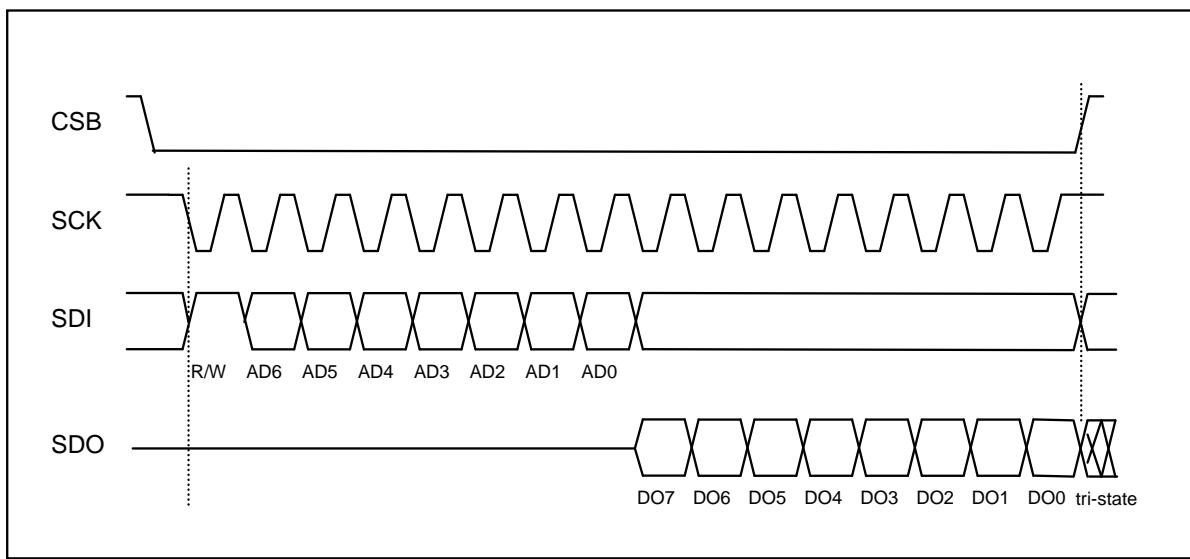
Figure 24: 4-wire basic SPI read sequence (mode ´11´)
The data bits are used as follows:
Bit0: Read/Write bit. When 0, the data SDI is written into the chip. When 1, the data SDO from the chip is read.
Bit1-7: Address AD(6:0).
| BOSCH | BMI160Data sheet | Page 93 |
Bit8-15: when in write mode, these are the data SDI, which will be written into the address. When in read mode, these are the data SDO, which are read from the address.
Multiple read operations are possible by keeping CSB low and continuing the data transfer. Only the first register address has to be written. Addresses are automatically incremented after each read access as long as CSB stays active low.
The principle of multiple read is shown in figure below:
| Control byte | Data byte | Data byte | Data byte | ||||||||||||||||||||||||||||||
| Start | RW | Register adress (02h) | Data register - adress 02h | Data register - adress 03h | Data register - adress 04h | Stop | |||||||||||||||||||||||||||
| CSB = 0 | 1 | 0 | 0 | 0 | 0 | 0 | 1 | 0 | X | X | X | X | X | X | X | X | X | X | X | X | X | X | X | X | X | X | X | X | X | X | X | X | CSB = 1 |
Figure 25: SPI multiple read
In SPI 3-wire configuration CSB (chip select low active), SCK (serial clock), and SDI (serial data input and output) pins are used. While SCK is high, the communication starts when the CSB is pulled low by the SPI master and stops when CSB is pulled high. SCK is also controlled by SPI master. SDI is driven (when used as input of the device) at the falling edge of SCK and should be captured (when used as the output of the device) at the rising edge of SCK.
The protocol as such is the same in 3-wire configuration as it is in 4-wire configuration. The basic operation wave-form (read or write access) for 3-wire configuration is depicted in the figure below:

Figure 26: 3-wire basic SPI read or write sequence (mode ´11´)
3.2.3 Primary I2C Interface
The I²C bus uses SCL (= SCx pin, serial clock) and SDA (= SDx pin, serial data input and output) signal lines. Both lines are connected to VDDIO externally via pull-up resistors so that they are pulled high when the bus is free.
The I²C addresses are identical to BMG160. The default I²C address of the device is 0b1101000 (0x68). It is used if the SDO pin is pulled to ´GND´. The alternative address 0b1101001 (0x69) is selected by pulling the SDO pin to ´VDDIO´.
| BOSCH | BMI160Data sheet | Page 94 |
The I²C interface of the BMI160 is compatible with the I²C Specification UM10204 Rev. 03 (19 June 2007), available at http://www.nxp.com. The BMI160 supports I²C standard mode and fast mode, only 7-bit address mode is supported. For $\mathsf { V } _ { \mathsf { D D I O } } = 1 . 2 \dot { \mathsf { V } }$ to 1.62 V the guaranteed voltage output levels are slightly relaxed as described in Table 1 of the electrical specification section.
BMI160 also supports an extended I²C mode that allows using clock frequencies up to 1 MHz. In this mode all timings of the fast mode apply and it additionally supports clock frequencies up to 1MHz.
The timing specification for I²C of the BMI160 is given in the following table:
Table 28: Primary I²C timings
| Parameter | Symbol | Condition | Min | Max | Units |
| Clock Frequency | $f_{SCL}$ | 1000 | kHz | ||
| SCL Low Period | $t_{LOW}$ | 1.3 | μs | ||
| SCL High Period | $t_{HIGH}$ | 0.6 | |||
| SDA Setup Time | $t_{SUDAT}$ | 0.1 | |||
| SDA Hold Time | $t_{HDDAT}$ | 0.0 | |||
| Setup Time for a repeated Start Condition | $t_{SUSTA}$ | 0.6 | |||
| Hold Time for a Start Condition | $t_{HDSTA}$ | 0.6 | |||
| Setup Time for a Stop Condition | $t_{SUSTO}$ | 0.6 | |||
| Time before a new Transmission can start | $t_{BUF}$ | low power mode | 400 | ||
| normal mode | 1.3 | ||||
| Idle time between write accesses, normal mode, standby mode, low-power mode | $t_{IDLE\_wacc\_n}$ m | low power mode | 400 | ||
| normal mode | 1.3 | ||||
| Idle time between write accesses, suspend mode, low-power mode | $t_{IDLE\_wacc\_s}$ um | 400 |
| BOSCH | BMI160Data sheet | Page 95 |
The figure below shows the definition of the I²C timings given in Table 28:
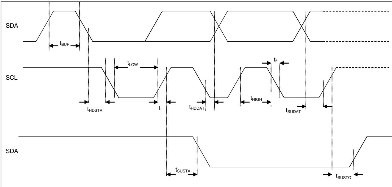
Figure 27: I²C timing diagram
The I²C protocol works as follows:
START: Data transmission on the bus begins with a high to low transition on the SDA line while SCL is held high (start condition (S) indicated by I²C bus master). Once the START signal is transferred by the master, the bus is considered busy.
STOP: Each data transfer should be terminated by a Stop signal (P) generated by master. The STOP condition is a low to HIGH transition on SDA line while SCL is held high.
ACKS: Each byte of data transferred must be acknowledged. It is indicated by an acknowledge bit sent by the receiver. The transmitter must release the SDA line (no pull down) during the acknowledge pulse while the receiver must then pull the SDA line low so that it remains stable low during the high period of the acknowledge clock cycle.
In the following diagrams these abbreviations are used:
| S | Start |
| P | Stop |
| ACKS | Acknowledge by slave |
| ACKM | Acknowledge by master |
| NACKM | Not acknowledge by master |
| RW | Read / Write |
A START immediately followed by a STOP (without SCL toggling from ´VDDIO´ to ´GND´) is not supported. If such a combination occurs, the STOP is not recognized by the device.
| BOSCH | BMI160Data sheet | Page 96 |
I²C write access:
I²C write access can be used to write a data byte in one sequence.
The sequence begins with start condition generated by the master, followed by 7 bits slave address and a write bit (RW = 0). The slave sends an acknowledge bit (ACKS = 0) and releases the bus. Then the master sends the one byte register address. The slave again acknowledges the transmission and waits for the 8 bits of data which shall be written to the specified register address. After the slave acknowledges the data byte, the master generates a stop signal and terminates the writing protocol.
Example of an I²C write access:
| Control byte | Data byte | |||||||||||||||||||||||||||
| Start | Slave Adress | RW | ACKS | Register adress (0x10) | ACKS | Data (0x09) | ACKS | Stop | ||||||||||||||||||||
| S | 1 | 1 | 0 | 1 | 0 | 0 | 0 | 0 | 0 | 1 | 1 | 1 | 0 | 0 | 0 | 0 | 1 | 1 | 0 | 1 | 0 | 1 | 0 | 1 | P | |||
Figure 28: I²C write
I²C read access:
I²C read access also can be used to read one or multiple data bytes in one sequence.
A read sequence consists of a one-byte I²C write phase followed by the I²C read phase. The two parts of the transmission must be separated by a repeated start condition (S). The I²C write phase addresses the slave and sends the register address to be read. After slave acknowledges the transmission, the master generates again a start condition and sends the slave address together with a read bit (RW = 1). Then the master releases the bus and waits for the data bytes to be read out from slave. After each data byte the master has to generate an acknowledge bit (ACKS = 0) to enable further data transfer. A NACKM (ACKS = 1) from the master stops the data being transferred from the slave. The slave releases the bus so that the master can generate a STOP condition and terminate the transmission.
The register address is automatically incremented and, therefore, more than one byte can be sequentially read out. Once a new data read transmission starts, the start address will be set to the register address specified since the latest I²C write command. By default the start address is set at 0x00. In this way repetitive multi-bytes reads from the same starting address are possible.
In order to prevent the I²C slave of the device to lock-up the I²C bus, a watchdog timer (WDT) is implemented. The WDT observes internal I²C signals and resets the I²C interface if the bus is locked-up by the BMI160. The activity and the timer period of the WDT can be configured through the bits i2c_wdt_en and i2c_wdt_sel at Register (0x70) NV_CONF.
Writing ´1´ (´0´) to Register (0x70) NV_CONF i2c_wdt_en activates (de-activates) the WDT. Writing ´0´ (´1´) to Register (0x70) NV_CONF i2c_wdt_en selects a timer period of 1 ms (50 ms).
| BOSCH | BMI160Data sheet | Page 97 |
Example of an I²C read access (reading gyro data):
| Control byte | ||||||||||||||||||
| Start | Slave Adress | RW | ACKS | dummy | Register adress (0x02) | ACKS | ||||||||||||
| S | 1 | 1 | 0 | 1 | 0 | 0 | 0 | 0 | X | 0 | 0 | 0 | 1 | 1 | 0 | 0 | ||
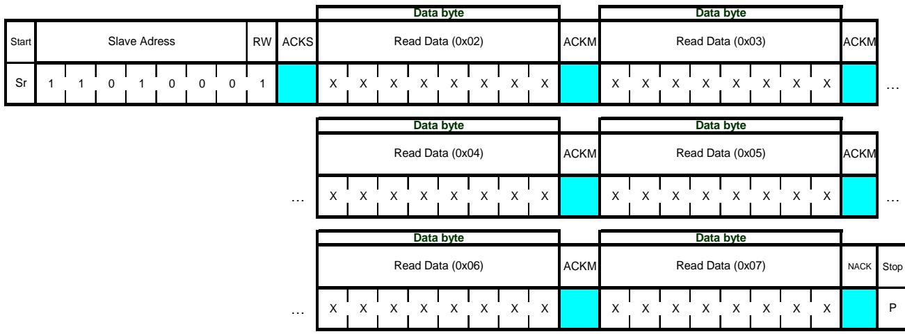
Figure 29: I²C multiple read
3.2.4 SPI and I²C Access Restrictions
In order to allow for the correct internal synchronization of data written to the BMI160, certain access restrictions apply for consecutive write accesses or a write/read sequence through the SPI as well as I2C interface. The required waiting period depends on whether the device is operating in normal mode or other modes.
As illustrated in the figure below, an interface idle time of at least 2 µs is required following a write operation when the device operates in normal mode. In suspend mode an interface idle time of least 450 µs is required5.

Figure 30: Post-Write Access Timing Constraints
| BOSCH | BMI160Data sheet | Page 98 |
3.3 Secondary Interface
The secondary interface can be used in two different classes of use cases:
Magnetometer Interface (I2C) for connecting to a MAG-sensor
In this case the secondary interface is used as a two-wire interface where an external sensor (MAG-sensor) would be connected as a slave to BMI160. The typical application is connecting a Bosch Sensortec geomagnetic sensor (BMM150).
In this case the secondary interface is used as a SPI interface where an external control unit is connected as a master to BMI160. External control unit can be e.g. OIS controllers.
The mapping for the secondary interface of the BMI160 is given in the following table:
Table 29: Mapping of the secondary interface pins
| Pin# | Name | I/O Type | Description | Connect to (secondary IF) | ||
| in SPI4W | in SPI3W | in I2C | ||||
| 2 | ASDx | Digital I/O | Secondary Magnetometer interface | MOSI | SISO | SDA |
| 3 | ASCx | Digital I/O | Secondary Magnetometer interface | SCK | SCK | SCL |
| 10 | OCSB | Digital in | Secondary OIS interface | CSB | CSB | DNC |
| 11 | OSDO | Digital out | Secondary OIS interface | MISO | DNC | DNC |
3.3.1 Magnetometer connected to secondary interface
The BMI160 allows attaching an external sensor (MAG-sensor) to a BMI160 via the secondary interface (magnetometer interface), as shown in Figure 21. The connection diagrams for the magnetometer interface are depicted in the chapter 4. The timings of the secondary I2C interface are the same as for the primary I2C interface, see chapter 3.2.3.
BMI160 acts as a master of the secondary interface, controls the data acquisition of the MAGsensor (slave of the secondary interface) and presents the data to the application processor (AP) in the user registers of the BMI160 through the primary interface. External pull-up resistors need to be connected and no additional I2C master or slave devices must be attached to the magnetometer interfaces.
The BMI160 autonomously reads out the sensor data from BMM150 without intervention of the AP and stores the data in its data registers (per default) and FIFO (see Register (0x46-0x47) FIFO_CONFIG). The initial setup of the BMM150 after power-on is done through indirect addressing in the BMI160. From a system perspective the initialization for BMM150 when attached to BMI160 should be possible within 100ms.
The main benefits of the magnetometer interface are:
to synchronize sensor data from the magnetometer and the IMU; this improves the quality of sensor data fusion
to use the IMU-FIFO for storing the magnetometer data; this can be important for monitoring applications.
| BOSCH | BMI160Data sheet | Page 99 |
3.3.1.1 Configuration options of the secondary interface as magnetometer interface
The secondary interface configured as a magnetometer interface is a I2C master interface supporting Fast-Mode I²C communication.
In this mode the ASCx pad is output only, since both master and slave don’t support clock stretching and only master can drive the clock. ASCx is configured as push-pull output when magnetometer interface is enabled. The ASDx pad is used for data transfer between master and slave devices and is bidirectional.
There are two basis configurations of the magnetometer interface that can be configured using the Register (0x4B-0x4F) MAG_IF: Setup mode and Data mode.
- Setup mode (also manual mode): In this mode, the application processor can access every f h h d h d f h h d dd h mode is usually used to configure the MAG-sensor and the way the secondary interface reads the data. The Setup mode has to be executed after each POR (power on reset) previous to the first data acquisition in Data mode (see below).
The Setup mode is enabled by setting the MAG_IF1<7> = 1. The magnetometer may be accessed through the primary interface using indirect addressing. The data for the I2C write to magnetometer is stored in MAG_IF4. MAG_IF2 defines the first address of the register to read (MAG_IF3 define the address for write access) in the magnetometer register map and triggers the operation itself, when the magnetometer interface is in normal mode.
For reads, the number of data bytes defined in mag_rd_burst in register MAG_IF1<0:1> are read from the magnetometer and written into the MAG_[X-Z] and RHALL fields of the register DATA. For write accesses, no burst write is supported, independent of the settings in mag_rd_burst in Register (0x4B-0x4F) MAG_IF.
When a read or write operation is triggered by writing to MAG_IF2 or MAG_IF3, a bit indicator mag_man_op in
Register (0x1B) STATUS is set and when the operation is completed it is automatically reset. In case a measurement trigger is necessary (i.e. BMM150), the MAG-sensor register address and data should be specified by writing the appropriate value (i.e. 0x06) in the required external sensor register address (i.e. 0x44) through the last indirect write access in setup mode before changing to Data mode.
The time delay between triggering a magnetometer measurement and reading the measured data is specified in mag_offset in MAG_IF1.
The data rate used for the autonomous reading of the MAG-sensor data in Data mode should be first specified by configuring the mag_odr in Register (0x44) MAG_CONF<0:3>.
- Data mode: When collecting sensor data in Data mode, the BMI160 autonomously triggers the measurement of the magnetometer, reads the data from the magnetometer and copies it into the BMI160 user register. Once the data mode is running, the application processor can access the data of the secondary sensor simply by reading from the BMI160 user Register (0x04-0x17) DATA_0 Register (0x04-0x17) DATA_7 0x0b. In case of BMM150, the data read is the magnetometer data MAG_[X-Z] and Hall resistance RHALL. The data mode mode is enabled by setting the MAG_IF_1<7> = 0.
MAG_IF2 defines the lowest address of the register data bytes to read from the MAG-sensor and the data will be stored in the BMI160 register MAG-DATA. The data ready status is set via drdy_mag in
| BOSCH | BMI160Data sheet | Page 100 |
Register (0x1B) STATUS, but this operation never clears drdy_mag, it is typically cleared through reading the Register (0x04-0x17) DATA. If DRDY is not active the error bit mag_drdy_err in Register (0x02) ERR_REG is set. MAG_IF3 defines the register address of the magnetometer to start a measurement in forced mode in the magnetometer register map. Reading of the data is done in a single I2C read operation with a burst length of 8 bytes.
3.3.2 Camera module connected to secondary interface for OIS
BMI160 supports specific optical image stabilization (OIS) applications with a dedicated interface. This interface is used for direct access to pre-filtered gyroscope data with minimum latency. Pre filtered gyroscope data is available at output data rate (ODR) of 6.4 kHz and can be read out via OIS fast mode SPI interface at 10MHz maximum speed.
The OIS SPI interface supports 3-wire SPI as well as 4-wire SPI.
The timings of the secondary SPI interface are the same as for the primary SPI interface, see chapter 3.2.2. The connection diagrams are depicted in chapter 4.3.
4. Pin-out and Connection diagrams
4.1 Pin-out
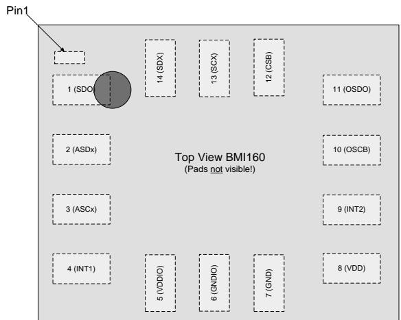
Figure 31: Pin-out top view

Figure 32: Pin-out bottom view
Table 30: BMI160 Pin-out and pin connections are described in the table below
| Pin# | Name | I/O Type | Interface | Description |
| 1 | SDO | Digital I/O | Primary | Serial data output in SPIAddress select in I2C mode |
| 2 | ASDx | Digital I/O | Secondary | Magnetometer interface**) |
| 3 | ASCx | Digital I/O | Secondary | Magnetometer interface**) |
| 4 | INT1 | Digital I/O | Primary | Interrupt pin 1 *) |
| 5 | VDDIO | Supply | - | Digital I/O supply voltage(1.2 ... 3.6V) |
| 6 | GNDIO | Ground | - | Ground for I/O |
| 7 | GND | Ground | - | Ground for digital & analog |
| 8 | VDD | Supply | - | Power supply analog & digital domain (1.71V – 3.6V) |
| 9 | INT2 | Digital I/O | Primary | Interrupt pin 2 *) |
| 10 | OCSB | Digital in | Secondary | OIS interface**) |
| 11 | OSDO | Digital out | Secondary | OIS interface**) |
| 12 | CSB | Digital in | Primary | Chip select for SPI mode / Protocol selection pin |
| 13 | SCx | Digital in | Primary | SCK for SPI serial clockSCL for I2C serial clock |
| 14 | SDx | Digital I/O | Primary | SDA serial data I/O in I2CMOSI serial data input in SPI 4WSISO serial data I/O in SPI 3W |
*) If INT1 and/or INT2 are not used, please do not connect them (DNC)
**) If pins ASDX, ASCX, OCSB, OSDO are not used, they will be high impedance status
| BOSCH | BMI160Data sheet | Page 102 |
4.2 Connection diagrams to use primary interface only 4.2.1 I2C as primary interface

Figure 33: Only I2C as primary interface
4.2.2 SPI 3-wire as primary interface

Figure 34: Only SPI 3-wire as primary interface
4.2.3 SPI 4-wire as primary interface
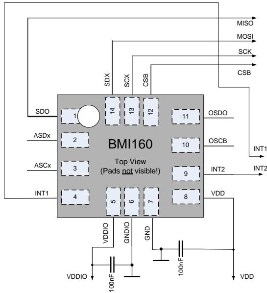
Figure 35: Only SPI 4-wire as primary interface
4.3 Connection diagrams to use additional secondary interface 4.3.1 Primary SPI 4-wire and secondary magnetometer interface (I2C)
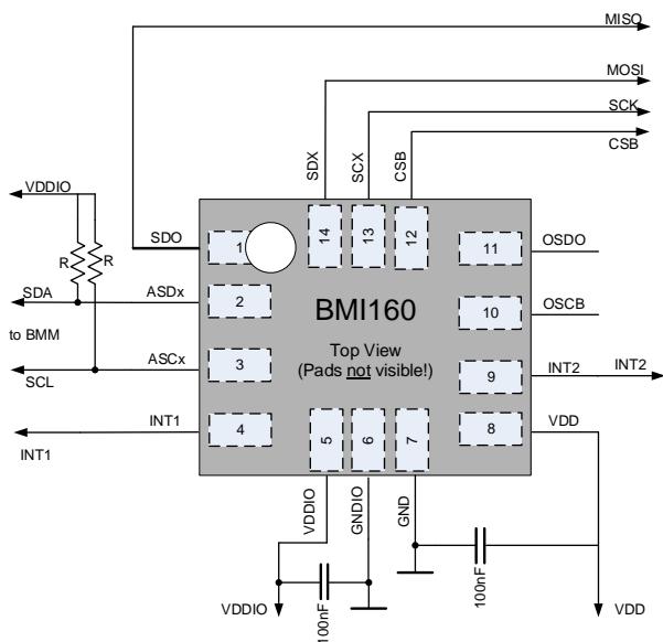
Figure 36: Using SPI 4-wire and the magnetometer interface
4.3.2 Primary SPI 3-wire and secondary magnetometer interface $( \mathbf { \boldsymbol { l } } ^ { 2 } \mathbf { \boldsymbol { C } } )$
Figure 37: Using SPI 3-wire and the magnetometer interface
4.3.3 Primary I2C and secondary magnetometer interface $( \mathbf { l } ^ { 2 } \mathbf { C } )$

Figure 38: Using ${ \mathsf { I } } ^ { 2 } { \mathsf { C } }$ and the magnetometer interface
| BOSCH | BMI160Data sheet | Page 105 |
4.3.4 Primary I2C and secondary 4-wire SPI as OIS interface
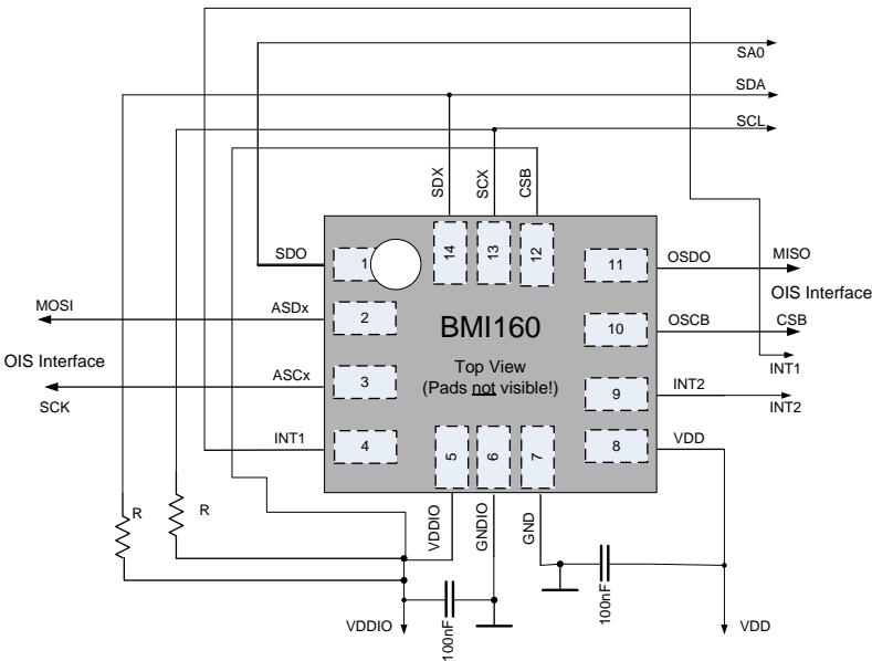
Figure 39: Using I2C and 4-wire SPI as OIS interface
4.3.5 Primary I2C and secondary 3-wire SPI as OIS interface

Figure 40: Using I2C and 3-wire SPI as OIS interface
| BOSCH | BMI160Data sheet | Page 106 |
5. Package
5.1 Outline Dimensions
The package dimension is LGA 2.5mm x 3.0mm x 0.83mm.
Unit of the following drawing is mm. Note: Unless otherwise specified tolerance = decimal ±0.05 mm.

Figure 41: Packaging outline dimensions
Note: Pin1 marker is internally connected to Pin1. It must not be connected to a different signal than Pin1.
| BOSCH | BMI160Data sheet | Page 107 |
5.2 Sensing axes orientation
If the sensor is accelerated and/or rotated in the indicated directions, the corresponding channels of the device will deliver a positive acceleration and/or yaw rate signal (dynamic acceleration). If the sensor is at rest without any rotation and the force of gravity is acting contrary to the indicated directions, the output of the corresponding acceleration channel will be positive and the corresponding gyroscope channel will be “zero” (static acceleration).
Example: If the sensor is at rest or at uniform motion in a gravity field according to the figure given below, the output signals are:
± 0g for the $\tt X A C C$ channel
± 0g for the $\textsf { Y A C C }$ channel
$\mathsf { a n d } \pm 0 ^ { \circ } /$ sec for the $\Omega \times$ GYR channel
+ 1g for the $Z \mathsf { A C C }$ channel
$\mathsf { a n d } \pm 0 ^ { \circ } /$ /sec for the $\Omega \gamma$ GYR channel
$\mathtt { a n d } \pm 0 % \mathtt { e c }$ for the $\Omega _ { Z }$ GYR channel

Figure 42: definition of sensing axes orientation
For reference the figure below shows the Android device orientation with an integrated BMI160.

Figure 43: Android axis definition with BMI160
| BOSCH | BMI160Data sheet | Page 108 |
5.3 Landing pattern recommendation
The following landing pad recommendation is given for maximum stability of the solder connections.

Figure 44: Landing pattern recommendation for BMI160
Note: Pin1 marker is internally connected to Pin1. It must not be connected to a different signal than Pin1.
The size of the landing pads may be further reduced in order to minimize solder-stress induced effects if sufficient control over the soldering process is given. Please contact your sales representative for further details.
| BOSCH | BMI160Data sheet | Page 109 |
5.4 Marking
5.4.1 Mass production marking
Table 31: Marking of mass samples
| Labeling | Name | Symbol | Remark |
| Counter ID | CCC | 3 alphanumeric digits, variable to generate trace-code | |
| <img src="./images/406919b69befcd23caf56795d37f86fc37a9ad705c982ae91849dbdd81c5eba6.jpg"/> | First letter of second row | V | Product identifier V = “T” denoting BMI160 |
| Second letter of second row | L | Internal use | |
| Pin 1 identifier | ● | -- |
5.4.2 Engineering samples
Table 32: Marking of engineering samples
| Labeling | Name | Symbol | Remark |
| <img src="./images/865dabbad9872842aef16db0244f7521e5458e16ac56b60293cabc0348c53077.jpg"/> | Internal ID | VLE | Product identifier V = “T” denoting BMI160 and “E” denotes engineering statusL – internal use |
| Second row | CC | -C - internal revision ID | |
| Pin 1 identifier | ● | -- | |
| BOSCH | BMI160Data sheet | Page 110 |
5.5 Soldering guidelines
The moisture sensitivity level of the BMI160 sensors corresponds to JEDEC Level 1, see also
IPC/JEDEC J-STD-020E “Joint Industry Standard: Moisture/Reflow Sensitivity Classification for non-hermetic Solid State Surface Mount Devices”
IPC/JEDEC J-STD-033D “Joint Industry Standard: Handling, Packing, Shipping and Use of Moisture/Reflow Sensitive Surface Mount Devices”
The sensor fulfils the lead-free soldering requirements of the above-mentioned IPC/JEDEC standard, i.e. reflow soldering with a peak temperature up to 260°C.
| Profile Feature | Pb-Free Assembly | |
| Average Ramp-Up Rate( $Ts_{max}$ to $Tp$ ) | 3°C/second max. | |
| Preheat- Temperature Min ( $Ts_{min}$ )- Temperature Max ( $Ts_{max}$ )- Time ( $ts_{min}$ to $ts_{max}$ ) | 150 °C200 °C60-180 seconds | |
| Time maintained above:- Temperature ( $T_L$ )- Time ( $t_L$ ) | 217 °C60-150 seconds | |
| Peak/Classification Temperature (Tp) | 260 °C | |
| Time within 5 °C of actual PeakTemperature (tp) | 20-40 seconds | |
| Ramp-Down Rate | 6 °C/second max. | |
| Time 25 °C to Peak Temperature | 8 minutes max. |
Note 1: All temperatures refer to topside of the package, measured on the package body surface

Figure 45: Soldering profile
| BOSCH | BMI160Data sheet | Page 111 |
5.6 Handling instructions
Micromechanical sensors are designed to sense acceleration with high accuracy even at low amplitudes and contain highly sensitive structures inside the sensor element. The MEMS sensor can tolerate mechanical shocks up to several thousand g’s. However, these limits might be exceeded in conditions with extreme shock loads such as e.g. hammer blow on or next to the sensor, dropping of the sensor onto hard surfaces etc.
We recommend to avoid g-forces beyond the specified limits during transport, handling and mounting of the sensors in a defined and qualified installation process.
This device has built-in protections against high electrostatic discharges or electric fields (e.g. 2kV HBM); however, anti-static precautions should be taken as for any other CMOS component. Unless otherwise specified, proper operation can only occur when all terminal voltages are kept within the supply voltage range. Unused inputs must always be tied to a defined logic voltage level.
5.7 Tape and reel specification
The BMI160 is shipped in a standard cardboard box.
The box dimension for 1 reel is: L × W × H = 35 cm × 35 cm × 6 cm.
BMI160 quantity: 5,000pcs per reel, please handle with care.

$$
\mathrm{A} _ {0} = 3. 3 0, \mathrm{B} _ {0} = 2. 8 0, \mathrm{K} _ {0} = 1. 1 0
$$
Note:
Tolerances unless noted: ±0.1
Sprocket hole pitch cumulative tolerance ±0.1
• Camber in compliance with ElA481
Pocket position relative to sprocket hole measured as true position of pocket, not pocket hole
A0 and B0 are calculated on a plane at a distance “R” above the bottom of the pocket
Figure 46: Tape and reel dimensions in mm
5.7.1 Orientation within the reel
→ Processing direction →

Figure 47: Orientation of the BMI160 devices relative to the tape
5.8 Environmental safety
The BMI160 sensor meets the requirements of the EC restriction of hazardous substances (RoHS) directive, see also:
RoHS – Directive 2011/65/EU and its amendments, including the amendment 2015/863/EU on the restriction of the use of certain hazardous substances in electrical and electronic equipment.
5.8.1 Halogen content
The BMI160 is halogen-free. For more details on the analysis results please contact your Bosch Sensortec representative.
5.8.2 Multiple sourcing
Within the scope of Bosch Sensortec’s ambition to improve its products and secure the mass product supply, Bosch Sensortec employs multiple sources in the supply chain.
While Bosch Sensortec takes care that all of technical parameters are described above are 100% identical for all sources, there can be differences in device marking and bar code labeling.
However, as secured by the extensive product qualification process of Bosch Sensortec, this has no impact to the usage or to the quality of the product.
| BOSCH | BMI160Data sheet | Page 113 |
6. Legal disclaimer
6.1 Engineering samples
Engineering Samples are marked with an asterisk (*), (E) or (e). Samples may vary from the valid technical specifications of the product series contained in this data sheet. They are therefore not intended or fit for resale to third parties or for use in end products. Their sole purpose is internal client testing. The testing of an engineering sample may in no way replace the testing of a product series. Bosch Sensortec assumes no liability for the use of engineering samples. The Purchaser shall indemnify Bosch Sensortec from all claims arising from the use of engineering samples.
6.2 Product use
Bosch Sensortec products are developed for the consumer goods industry. They may only be used within the parameters of this product data sheet. They are not fit for use in life-sustaining or safety-critical systems. Safety-critical systems are those for which a malfunction is expected to lead to bodily harm, death or severe property damage. In addition, they shall not be used directly or indirectly for military purposes (including but not limited to nuclear, chemical or biological proliferation of weapons or development of missile technology), nuclear power, deep sea or space applications (including but not limited to satellite technology).
Bosch Sensortec products are released on the basis of the legal and normative requirements relevant to the Bosch Sensortec product for use in the following geographical target market: BE, BG, DK, DE, EE, FI, FR, GR, IE, IT, HR, LV, LT, LU, MT, NL, AT, PL, PT, RO, SE, SK, SI, ES, CZ, HU, CY, US, CN, JP, KR, TW. If you need further information or have further requirements, please contact your local sales contact.
The resale and/or use of Bosch Sensortec products are at the purchaser’s own risk and his own responsibility. The examination of fitness for the intended use is the sole responsibility of the purchaser.
The purchaser shall indemnify Bosch Sensortec from all third party claims arising from any product use not covered by the parameters of this product data sheet or not approved by Bosch Sensortec and reimburse Bosch Sensortec for all costs in connection with such claims.
The purchaser accepts the responsibility to monitor the market for the purchased products, particularly with regard to product safety, and to inform Bosch Sensortec without delay of all safety-critical incidents.
6.3 Application examples and hints
With respect to any examples or hints given herein, any typical values stated herein and/or any information regarding the application of the device, Bosch Sensortec hereby disclaims any and all warranties and liabilities of any kind, including without limitation warranties of non-infringement of intellectual property rights or copyrights of any third party. The information given in this document shall in no event be regarded as a guarantee of conditions or characteristics. They are provided for illustrative purposes only and no evaluation regarding infringement of intellectual property rights or copyrights or regarding functionality, performance or error has been made.
| BOSCH | BMI160Data sheet | Page 114 |
7. Document history and modifications
| Rev. No | Chapter | Description of modification/changes | Date |
| 0.9 | 2.2.4 | Table 8 updated | $16^{th}$ Oct 2018 |
| 2.5.1.52.5.2.4 | Explanation updated how to configure external interrupt tags, Description of FIFO config frame updated | ||
| 2.7 | Description of Step Counter updatedUpdated hyperlink | ||
| 2.112.11.37 | Register description updated | ||
| 2.5.1.5 | Description updated | ||
| 2.4.1 | Table 13 updated | ||
| 2.6.2 | Flow diagram updated | ||
| 3.2.2 | SDO output delay time added | ||
| 3.3.2 | Max. speed of OIS I/F updated | ||
| 2.2.4 | Current consumption in Table 8 corrected | ||
| 1.1 | Current consumption in Table 1 corrected | ||
| Current consumption in General Description corrected | |||
| 3.3.13.3.1.1 | External pull-up resistors need to be connectedUpdated content | ||
| 2.11.15 | Updated ODR formula | ||
| 4.3.14.3.24.3.3 | Updated pull-ups in the recommended connection diagrams | ||
| 5.3 | Updated landing pattern | ||
| 2.6.72.11.24 | Updated low-g feature descriptionUpdated register description | ||
| 4.1 | Updated comments in Table 30 | ||
| 1.0 | 1, 2.2, 2.42.11.253.3, 4.15.5, 5.86 | Updated Table 1, 9 and 13Updated descriptionUpdated typos in tables 29 and 30Updated referencesDisclaimer update | $25^{th}$ Nov 2020 |
Bosch Sensortec GmbH
Gerhard-Kindler-Strasse 8
72770 Reutlingen / Germany
Modifications reserved | Printed in Germany
Subject to change without notice
Document number: BST-BMI160-DS000-09
Revision_1.0_112020
Figures and diagrams from the PDF
Preview the extracted datasheet assets and open any image in a separate tab for closer inspection.


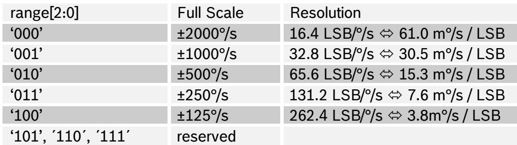
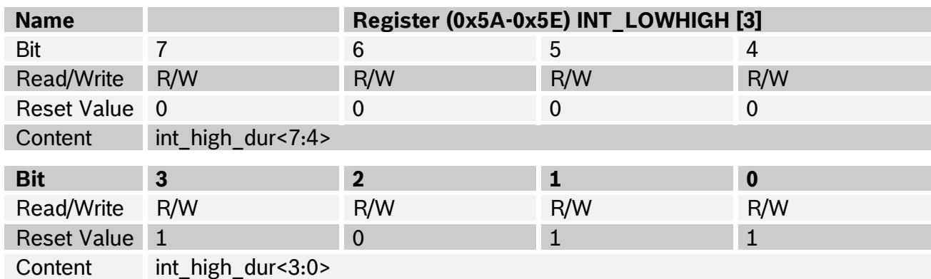
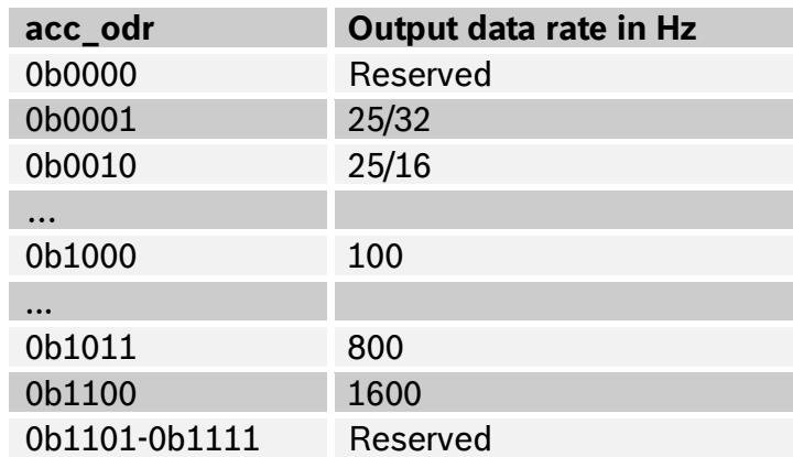

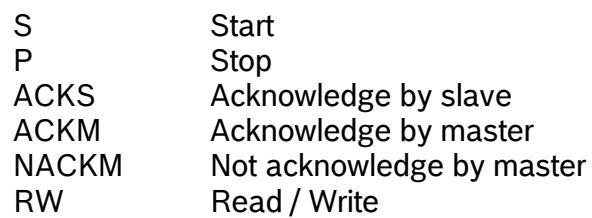
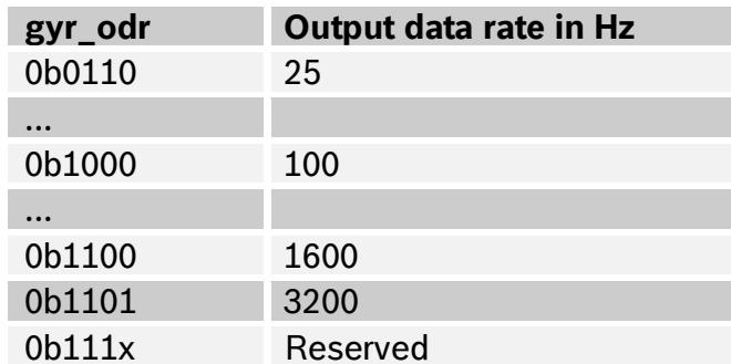








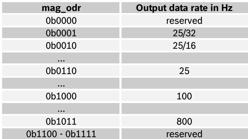
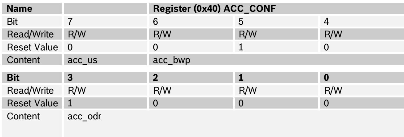
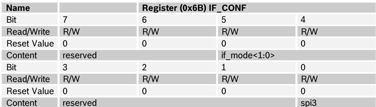


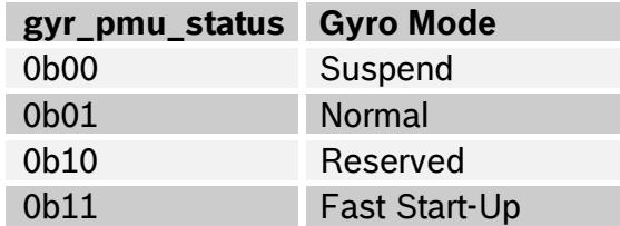

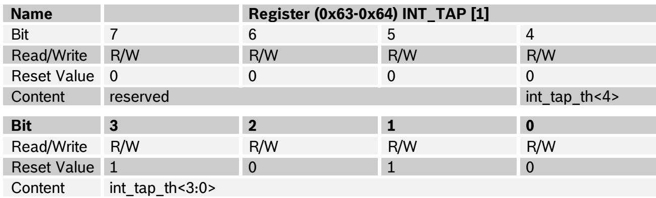

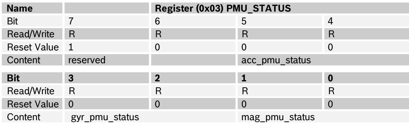
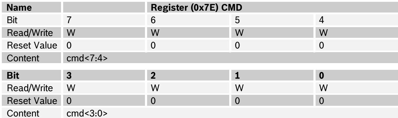
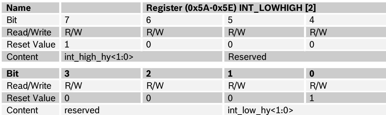
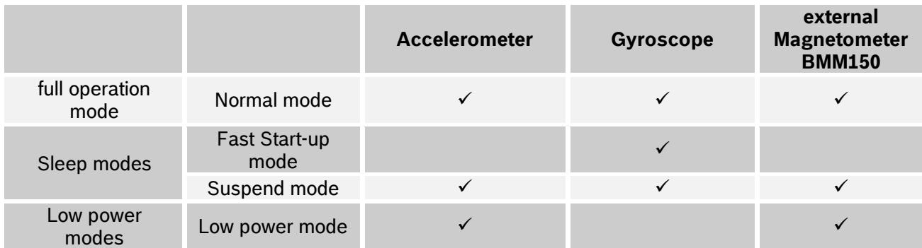

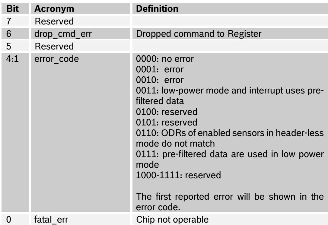


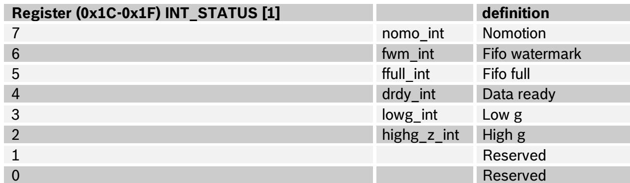



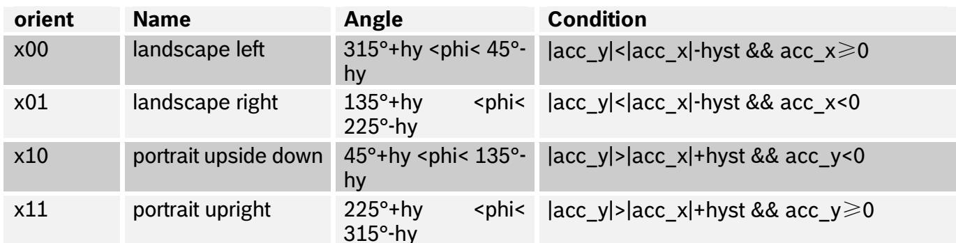

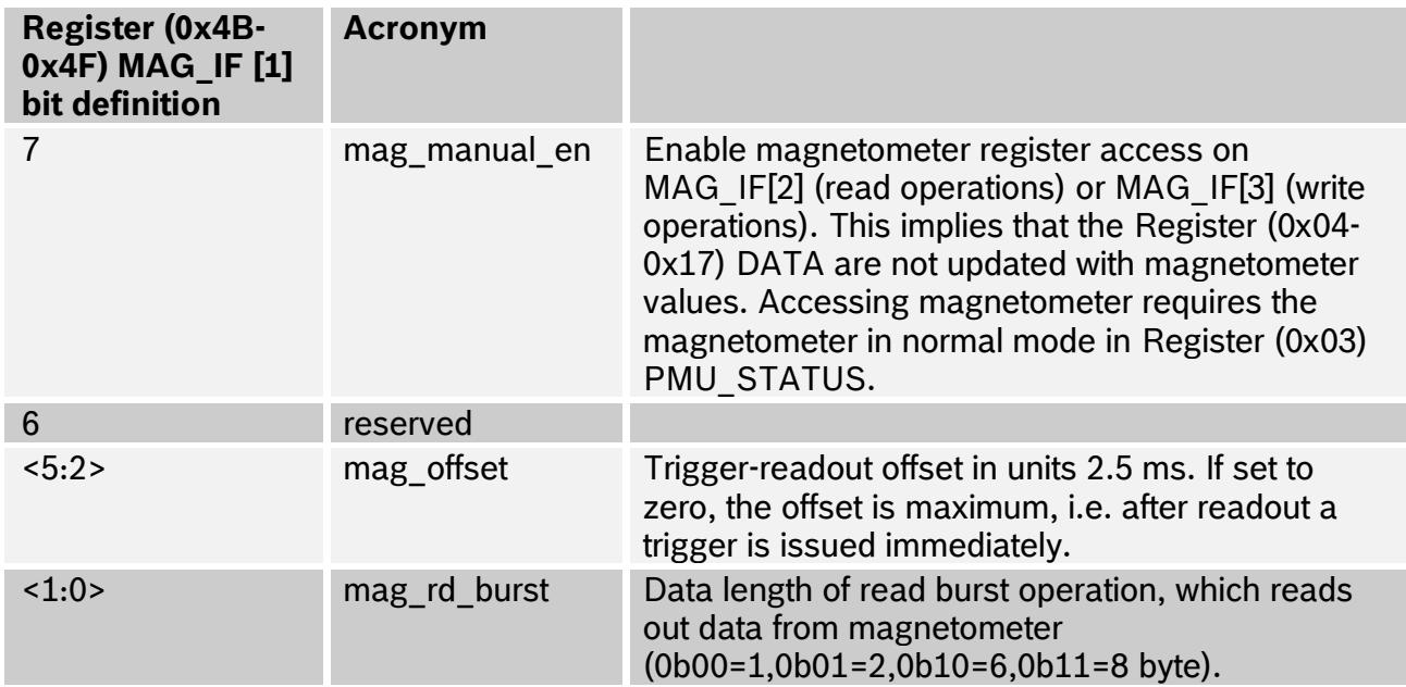



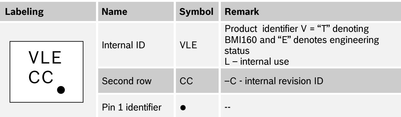

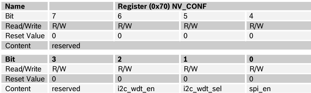
Use this datasheet from any agent
Send the page, markdown, chunks, or search endpoint to ChatGPT, Claude, embedr-app, or your own tooling.