
Analog Devices MAX98357AETE+T I2S Class-D Audio Amplifier
MAX98357AETE+T is a 16-TQFN I2S/TDM-input mono filterless Class-D speaker amplifier IC with integrated DAC, 2.5 V to 5.5 V supply operation, and no MCLK requirement.
General Description
The MAX98357A/MAX98357B is an easy-to-use, low-cost, digital pulse-code modulation (PCM) input Class D amplifier that provides industry-leading Class AB audio performance with Class D efficiency. The digital audio interface automatically recognizes up to 35 different PCM and TDM clocking schemes which eliminates the need for I2C programming. Operation is further simplified by eliminating the need for an external MCLK signal that is typically used for PCM communication. Simply supply power, LRCLK, BCLK, and digital audio to generate audio! Furthermore, a novel pinout allows customers to use the cost-effective WLP package with no need for expensive vias (refer to Application Note 6643: Optimize Cost, Size, and Performance with MAX98357 WLP for more information).
The digital audio interface is highly flexible with the MAX98357A supporting I2S data and the MAX98357B supporting left-justified data. Both ICs support 8 channe time division multiplexed (TDM) data. The digital audio interface accepts specified sample rates between 8kHz and 96kHz for all supported data formats. The ICs can be configured to produce a left channel, right channel, or (left/2 + right/2) output from the stereo input data. The ICs operate using 16/24/32-bit data for I2S and left-justified modes as well as 16-bit or 32-bit data using TDM mode. The ICs eliminate the need for the external MCLK signal that is typically used for PCM communication. This reduces EMI and possible board coupling issues in addition to reducing the size and pin count of the ICs.
The ICs also feature a very high wideband jitter tolerance (12ns typ) on BCLK and LRCLK to provide robust operation.
Active emissions-limiting, edge-rate limiting, and overshoot control circuitry greatly reduce EMI. A filterless spread-spectrum modulation scheme eliminates the need for output filtering found in traditional Class D devices and reduces the component count of the solution.
The ICs are available in 9-pin WLP (1.345mm x 1.435mm x 0.64mm) and 16-pin TQFN (3mm x 3mm x 0.75mm) packages and are specified over the -40°C to +85°C temperature range.
Ordering Information appears at end of data sheet.
Functional Diagram appears at end of data sheet.
Features
● Single-Supply Operation (2.5V to 5.5V)
● 3.2W Output Power into 4Ω at 5V
● 2.4mA Quiescent Current
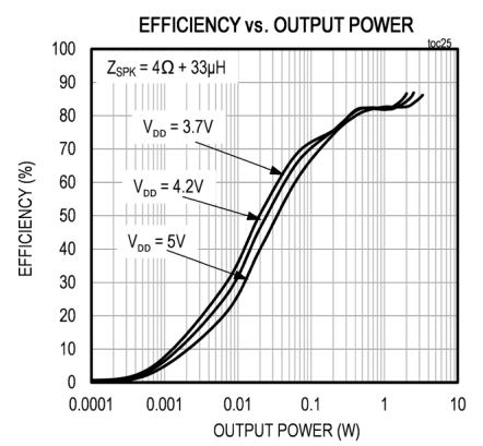
● 92% Efficiency $( \mathsf { R } _ { \mathsf { L } } = 8 \Omega , \mathsf { P } _ { \mathsf { O U T } } = 1 \mathsf { W } )$
● 22.8μVRMS Output Noise (AV = 15dB)
● Low 0.013% THD+N at 1kHz
● No MCLK Required
● Sample Rates of 8kHz to 96kHz
● Supports Left, Right, or (Left/2 + Right/2) Output
Sophisticated Edge Rate Control Enables Filterless Class D Outputs
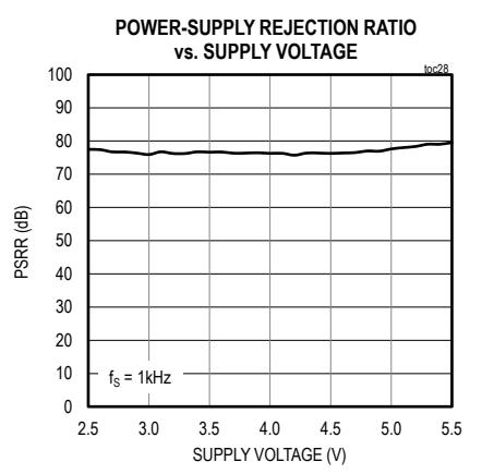
● 77dB PSRR at 1kHz
● Low RF Susceptibility Rejects TDMA Noise from GSM Radios
● Extensive Click-and-Pop Reduction Circuitry
● Robust Short-Circuit and Thermal Protection
● Available in Space-Saving Packages: 1.345mm x 1.435mm WLP (0.4mm Pitch) and 3mm x 3mm TQFN
● Solution Size with Single Bypass Capacitor is 4.32mm2
Applications
● Single Li-ion Cell/5V Devices
● Smart Speakers
● Notebook Computers
● IoT Devices
● Gaming Devices (Audio and Haptics)
● Smartphones
● Tablets
● Cameras
Simplified Block Diagram
19-6779; Rev 16; 2/26
TABLE OF CONTENTS
General Description....1
Features....1
Applications....1
Simplified Block Diagram....1
Absolute Maximum Ratings....4
Package Thermal Characteristics....4
Electrical Characteristics....4
Typical Operating Characteristics....9
Pin Configurations....15
Pin Description....15
Detailed Description....16
Digital Audio Interface Modes....16
MCLK Elimination....16
BCLK Jitter Tolerance....16
BCLK Polarity....16
LRCLK Polarity....16
Standby Mode....16
DAC Digital Filters....17
SD_MODE and Shutdown Operation....17
Startup....18
I2S and Left Justified Mode....19
TDM Mode....19
Class D Speaker Amplifier....28
Ultra-Low EMI Filterless Output Stage....28
Speaker Current Limit....28
Gain Selection....28
Click-and-Pop Suppression....28
Applications Information....29
Filterless Class D Operation....33
Power-Supply Input....33
Layout and Grounding....33
Functional Diagram....33
WLP Applications Information....34
Ordering Information....34
Package Information....35
Revision History....38
LIST OF FIGURES
Figure 1. I²S Audio Interface Timing Diagram (MAX98357A)....8
Figure 2. Left-Justified Audio Interface Timing Diagram (MAX98357B)....8
Figure 3. TDM Audio Interface Timing Diagram....8
Figure 4. SDMODE Resistor Connected Using Open-Drain Driver....18
Figure 5. SDMODE Resistor Connected Using Push-Pull Driver....18
Figure 6. Required startup sequence when using BCLK = 256kHz....19
Figure 7. MAX98357A I²S Digital Audio Interface Timing, 16-Bit Resolution....20
Figure 8. MAX98357A I²S Digital Audio Interface Timing, 32-Bit Resolution....21
Figure 9. MAX98357B Left-Justified Digital Audio Interface Timing, 16-Bit Resolution....22
Figure 10. MAX98357B Left-Justified Digital Audio Interface Timing, 32-Bit Resolution....23
Figure 11. MAX98357A TDM 16-Bit DAI Timing....24
Figure 12. MAX98357A TDM 32-Bit DAI Timing....25
Figure 13. MAX98357B TDM 16-Bit DAI Timing....26
Figure 14. MAX98357B TDM 32-Bit DAI Timing....27
Figure 15. EMI with 12in of Speaker Cable and No Output Filtering....28
Figure 16. Left-Channel PCM Operation with 6dB Gain....29
Figure 17. Left-Channel PCM Operation with 12dB Gain....29
Figure 18. Right-Channel PCM Operation with 6dB Gain....30
Figure 19. (Left/2 + Right/2) PCM Operation with 6dB Gain....30
Figure 20. Stereo PCM Operation Using Two ICs....31
Figure 21. Channel TDM Operation (Gain Fixed at 12dB)....32
Figure 22. WLP Pin Connect for set 12dB Gain Without Via....34
Figure 23. Example Layout Configured for Left-Channel Audio and Gain of 12dB....34
Figure 24. MAX98357A/MAX98357B WLP Ball Dimensions....34
LIST OF TABLES
Table 1. RMS Jitter Tolerance ..... 16
Table 2. BCLK Polarity..... 16
Table 3. LRCLK Polarity..... 16
Table 4. Digital Filter Settings ..... 17
Table 5. SD_MODE Control ..... 17
Table 6. Examples of SD_MODE Pullup Resistor Values..... 17
Table 7. TDM Mode Channel Selection ..... 20
Table 8. Gain Selection ..... 28
Tiny, Low-Cost, PCM Class D Amplifier with Class AB Performance
Absolute Maximum Ratings
VDD, LRCLK, BCLK, and DIN to GND....................-0.3V to +6V All Other Pins to GND .... ... -0.3V to $( \mathsf { V } _ { \mathsf { D D } } + 0 . 3 \mathsf { V } )$ Continuous Current In/Out of VDD/GND/OUT_.. ..±1.6A Continuous Input Current (all other pins) ....... ..±20mA Duration of OUT_ Short Circuit to GND or V …....Continuous Duration of OUTP Short to OUTN.... ...Continuous
Continuous Power Dissipation $( { \mathsf { T } } _ { \mathsf { A } } = + 7 0 ^ { \circ } { \mathsf { C } } )$ WLP (derate 13.7mW/°C above +70°C). .1096mW TQFN (derate 20.8mW/°C above +70°C).. .1666mW Junction Temperature.. ..+150°C Operating Temperature Range.. . -40°C to +85°C Storage Temperature Range.. . -65°C to +150°C Soldering Temperature (reflow)... ..+260°C Lead Temperature (soldering, 10s, TQFN) ..... ..+300°C
Stresses beyond those listed under “Absolute Maximum Ratings” may cause permanent damage to the device. These are stress ratings only, and functional operation of the device at these or any other conditions beyond those indicated in the operational sections of the specifications is not implied. Exposure to absolute maximum rating conditions for extended periods may affect device reliability.
(Note 1)Package Thermal Characteristics
WLP NLF
Junction-to-Ambient Thermal Resistance $( \Theta _ { \mathrm { J A } } ) \dots \dots \dots 7 3 ^ { \circ } \mathsf { C } N$ Junction-to-Case Thermal Resistance $( \Theta _ { \mathsf { J C } } )$ .....50°C/W
TQFN Junction-to-Ambient Thermal Resistance $( \Theta _ { \mathsf { J A } } )$ .....48°C/W Junction-to-Case Thermal Resistance $( \Theta _ { \mathsf { J C } } )$ ..7°C/W
Note 1: Package thermal resistances were obtained using the method described in JEDEC specification JESD51-7, using a four-laye board. For detailed information on package thermal considerations, refer to www.analog.com/thermal-tutorial.
Electrical Characteristics
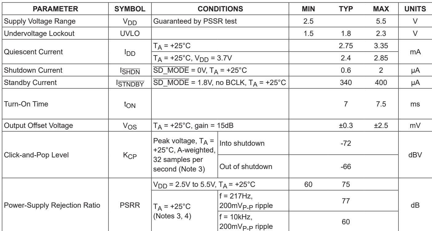
(VDD = 5V, VGND = 0V, GAIN_SLOT = VDD. BCLK = 3.072MHz, LRCLK = 48kHz, speaker loads $( Z _ { \mathsf { S P K } } )$ connected between OUTP and OUTN, ZSPK = ∞, $\mathsf { T } _ { \mathsf { A } } = \mathsf { T } _ { \mathsf { M I N } }$ to TMAX, unless otherwise noted. Typical values are at $\mathsf { T } _ { \mathsf { A } } = + 2 5 ^ { \circ } \mathsf { C } . )$ (Note 2)
| PARAMETER | SYMBOL | CONDITIONS | MIN | TYP | MAX | UNITS | |
| Supply Voltage Range | $V_{DD}$ | Guaranteed by PSSR test | 2.5 | 5.5 | V | ||
| Undervoltage Lockout | UVLO | 1.5 | 1.8 | 2.3 | V | ||
| Quiescent Current | $I_{DD}$ | $T_A = +25°C$ | 2.75 | 3.35 | mA | ||
| $T_A = +25°C, V_{DD} = 3.7V$ | 2.4 | 2.85 | |||||
| Shutdown Current | $I_{SHDN}$ | $\overline{SD\_MODE} = 0V, T_A = +25°C$ | 0.6 | 2 | μA | ||
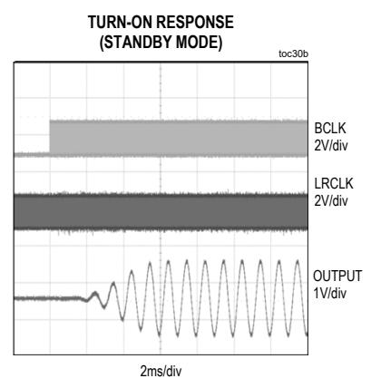
| Standby Current | $I_{STNDBY}$ | $\overline{SD\_MODE} = 1.8V, no BCLK, T_A = +25°C$ | 340 | 400 | μA | ||
| Turn-On Time | $t_{ON}$ | 7 | 7.5 | ms | |||
| Output Offset Voltage | $V_{OS}$ | $T_A = +25°C, gain = 15dB$ | ±0.3 | ±2.5 | mV | ||
| Click-and-Pop Level | $K_{CP}$ | Peak voltage, $T_A = +25°C, A-weighted, 32 samples per second (Note 3)$ | Into shutdown | -72 | dBV | ||
| Out of shutdown | -66 | ||||||
| Power-Supply Rejection Ratio | PSRR | $V_{DD} = 2.5V to 5.5V, T_A = +25°C$ | 60 | 75 | dB | ||
| $T_A = +25°C (Notes 3, 4)$ | f = 217Hz, 200mVP-P ripple | 77 | |||||
| f = 10kHz, 200mVP-P ripple | 60 | ||||||
Tiny, Low-Cost, PCM Class D Amplifier with Class AB Performance
Electrical Characteristics (continued)
(VDD = 5V, VGND = 0V, GAIN_SLOT = VDD. BCLK = 3.072MHz, LRCLK = 48kHz, speaker loads (ZSPK) connected between OUTP and $\mathsf { O U T N } , Z _ { \mathsf { S P K } } = \infty , \mathsf { T } _ { \mathsf { A } } = \mathsf { T } _ { \mathsf { M I N } }$ to TMAX, unless otherwise noted. Typical values are at $\mathsf { T } _ { \mathsf { A } } = + 2 5 ^ { \circ } \mathsf { C } . _ { \cdot }$ (Note 2)
| PARAMETER | SYMBOL | CONDITIONS | MIN | TYP | MAX | UNITS | |
| Output Power (Note 3) | POUT | THD+N 10%, gain = 12dB | ZSPK=4Ω+33μH | 3.2 | W | ||
| ZSPK=8Ω+68μH | 1.8 | ||||||
| ZSPK=8Ω+68μH, VDD=3.7V | 0.93 | ||||||
| THD+N = 1%, gain = 12dB | ZSPK=4Ω+33μH | 2.5 | |||||
| ZSPK=8Ω+68μH | 1.4 | ||||||
| ZSPK=8Ω+68μH, VDD=3.7V | 0.77 | ||||||
| Total Harmonic Distortion + Noise | THD+N | f = 1kHz, POUT=1W, TA=+25°C, ZSPK=4Ω+33μH, WLP | 0.02 | 0.06 | % | ||
| f = 1kHz, POUT=1W, TA=+25°C, ZSPK=4Ω+33μH, TQFN | 0.02 | ||||||
| f = 1kHz, POUT=0.5W, TA=+25°C, ZSPK=8Ω+68μH | 0.013 | ||||||
| Dynamic Range | DR | A-weighted, ZSPK=8Ω+33μH, VRMS=3.40V, 24- or 32-bit data | 103.5 | dB | |||
| Output Noise | VN | A-weighted, 24- or 32-bit data (Note 4) | 22.8 | μVRMS | |||
| Gain (Relative to a 2.1dBV Reference Level) | AV | GAIN_SLOT=GND through 100kΩ | 14.4 | 15 | 15.6 | dB | |
| GAIN_SLOT=GND | 11.4 | 12 | 12.6 | ||||
| GAIN_SLOT=unconnected | 8.4 | 9 | 9.6 | ||||
| GAIN_SLOT=VDD | 5.4 | 6 | 6.6 | ||||
| GAIN_SLOT=VDD through 100kΩ | 2.4 | 3 | 3.6 | ||||
| Current Limit | ILIM | 2.8 | A | ||||
| Efficiency | ε | ZSPK=8Ω+68μH, THD+N=10%, f=1kHz, gain=12dB | 92 | % | |||
| DAC Gain Error | 1 | % | |||||
| Frequency Response | -0.2 | +0.2 | dB | ||||
| Class D Switching Frequency | fOSC | 300 | kHz | ||||
| Spread-Spectrum Bandwidth | ±20 | kHz | |||||
| DAC DIGITAL FILTERS | |||||||
| VOICE MODE IIR LOWPASS FILTER (LRCLK < 30kHz) | |||||||
| Passband Cutoff | fPLP | Ripple limit cutoff | 0.443x fs | Hz | |||
| -3dB cutoff | 0.446x fs | ||||||
| Stopband Cutoff | fSLP | 0.464x fs | Hz | ||||
| Stopband Attenuation | f>fSLP | 75 | dB | ||||
Tiny, Low-Cost, PCM Class D Amplifier with Class AB Performance
Electrical Characteristics (continued)
(VDD = 5V, VGND = 0V, GAIN_SLOT = VDD. BCLK = 3.072MHz, LRCLK = 48kHz, speaker loads (ZSPK) connected between OUTP and OUTN, ZSPK = ∞, $\mathsf { T } _ { \mathsf { A } } = \mathsf { T } _ { \mathsf { M I N } }$ to TMAX, unless otherwise noted. Typical values are at $\mathsf { T } _ { \mathsf { A } } = + 2 5 ^ { \circ } \mathsf { C } .$ ) (Note 2)
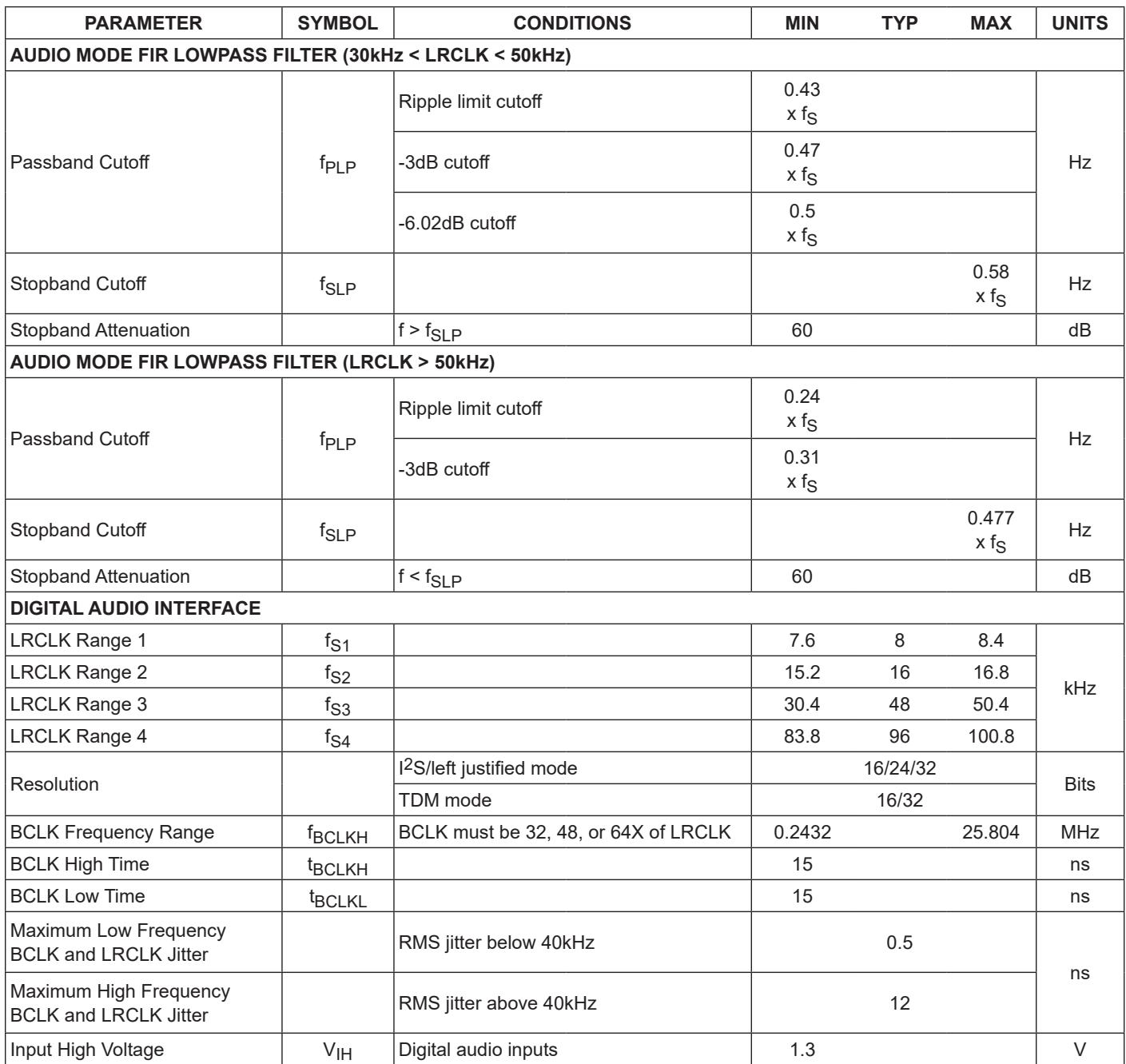
| PARAMETER | SYMBOL | CONDITIONS | MIN | TYP | MAX | UNITS |
| AUDIO MODE FIR LOWPASS FILTER (30kHz < LRCLK < 50kHz) | ||||||
| Passband Cutoff | $f_{PLP}$ | Ripple limit cutoff | 0.43x $f_S$ | Hz | ||
| -3dB cutoff | 0.47x $f_S$ | |||||
| -6.02dB cutoff | 0.5x $f_S$ | |||||
| Stopband Cutoff | $f_{SLP}$ | 0.58x $f_S$ | Hz | |||
| Stopband Attenuation | f > $f_{SLP}$ | 60 | dB | |||
| AUDIO MODE FIR LOWPASS FILTER (LRCLK > 50kHz) | ||||||
| Passband Cutoff | $f_{PLP}$ | Ripple limit cutoff | 0.24x $f_S$ | Hz | ||
| -3dB cutoff | 0.31x $f_S$ | |||||
| Stopband Cutoff | $f_{SLP}$ | 0.477x $f_S$ | Hz | |||
| Stopband Attenuation | f < $f_{SLP}$ | 60 | dB | |||
| DIGITAL AUDIO INTERFACE | ||||||
| LRCLK Range 1 | $f_{S1}$ | 7.6 | 8 | 8.4 | kHz | |
| LRCLK Range 2 | $f_{S2}$ | 15.2 | 16 | 16.8 | ||
| LRCLK Range 3 | $f_{S3}$ | 30.4 | 48 | 50.4 | ||
| LRCLK Range 4 | $f_{S4}$ | 83.8 | 96 | 100.8 | ||
| Resolution | I2S/left justified mode | 16/24/32 | Bits | |||
| TDM mode | 16/32 | |||||
| BCLK Frequency Range | $f_{BCLKH}$ | BCLK must be 32, 48, or 64X of LRCLK | 0.2432 | 25.804 | MHz | |
| BCLK High Time | $t_{BCLKH}$ | 15 | ns | |||
| BCLK Low Time | $t_{BCLKL}$ | 15 | ns | |||
| Maximum Low Frequency BCLK and LRCLK Jitter | RMS jitter below 40kHz | 0.5 | ns | |||
| Maximum High Frequency BCLK and LRCLK Jitter | RMS jitter above 40kHz | 12 | ||||
| Input High Voltage | $V_{IH}$ | Digital audio inputs | 1.3 | V | ||
Tiny, Low-Cost, PCM Class D Amplifier with Class AB Performance
Electrical Characteristics (continued)
$( \mathsf { V } _ { \mathsf { D D } } = 5 \mathsf { V } , \mathsf { V } _ { \mathsf { G N D } } = 0 \mathsf { V } ,$ GAIN_S $_ \mathsf { O T } = \mathsf { V } _ { \mathsf { D D } }$ . BCLK = 3.072MHz, LRCLK = 48kHz, speaker loads $( \mathsf { Z } \mathsf { s p } \mathsf { \kappa } )$ connected between OUTP and $\mathsf { O U T N } , Z _ { \mathsf { S P K } } = \infty , \mathsf { T } _ { \mathsf { A } } = \mathsf { T } _ { \mathsf { M I N } }$ to ${ \mathsf { T } } _ { { \mathsf { M A X } } } ,$ unless otherwise noted. Typical values are at $\mathsf { T } _ { \mathsf { A } } = + 2 5 ^ { \circ } \mathsf { C } . _ { \cdot }$ (Note 2)
| PARAMETER | SYMBOL | CONDITIONS | MIN | TYP | MAX | UNITS |
| Input Low Voltage | $V_{IL}$ | Digital audio inputs | 0.6 | V | ||
| Input Leakage Current | $I_{IH}, I_{IL}$ | $V_{IN} = 0V, V_{DD} = 5.5V, T_A = +25°C$ | -1 | +1 | μA | |
| Input Capacitance | $C_{IN}$ | 3 | pF | |||
| DIN to BCLK Setup Time | $t_{SETUP}$ | 10 | ns | |||
| LRCLK to BCLK Setup Time | $t_{SYNCSET}$ | 10 | ns | |||
| DIN to BCLK Hold Time | $t_{HOLD}$ | 10 | ns | |||
| LRCLK to BCLK Hold Time | $t_{SYNCHOLD}$ | 10 | ns | |||
| SD_MODE COMPARATOR TRIP POINTS | ||||||
| B0 | See SD_MODE and shutdown operation for details | 0.08 | 0.16 | 0.355 | V | |
| B1 | 0.65 | 0.77 | 0.825 | |||
| B2 | 1.245 | 1.4 | 1.5 | |||
| SD_MODE Pulldown Resistor | $R_{PD}$ | 92 | 100 | 108 | kΩ | |
| GAIN COMPARATOR TRIP POINTS | ||||||
| V_GAIN_SLOT | $A_V = 3dB gain$ | 0.65 x $V_{DD}$ | 0.85 x $V_{DD}$ | V | ||
| $A_V = 6dB gain$ | 0.9 x $V_{DD}$ | $V_{DD}$ | ||||
| $A_V = 9dB gain$ | 0.4 x $V_{DD}$ | 0.6 x $V_{DD}$ | ||||
| $A_V = 12dB gain$ | 0 | 0.1 x $V_{DD}$ | ||||
| $A_V = 15dB gain$ | 0.15 x $V_{DD}$ | 0.35 x $V_{DD}$ | ||||
Note 2: 100% production tested at $\mathsf { T } _ { \mathsf { A } } = + 2 5 ^ { \circ } \mathsf { C }$ . Specifications over temperature limits are guaranteed by design.
Note 3: Class D amplifier testing performed with a resistive load in series with an inductor to simulate an actual speaker load. For $\mathsf { R } _ { \mathsf { L } } = 8 \Omega , \mathsf { L } _ { \mathsf { L } } = 6 8 \mu \mathsf { H } . \mathsf { F o r } \mathsf { R } _ { \mathsf { L } } = 4 \Omega , \mathsf { L } _ { \mathsf { L } } = 3 3 \mu \mathsf { H } .$
Note 4: Digital silence used for input signal.
Note 5: Dynamic range measured using the EIAJ method. -60dBFS 1kHz output signal, A-weighted, and normalized to 0dBFS. f = 20Hz to 20kHz.

Figure 1. I2S Audio Interface Timing Diagram (MAX98357A)
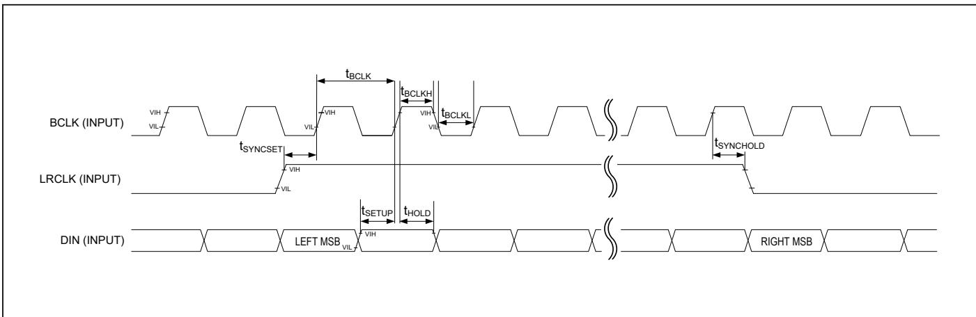
Figure 2. Left-Justified Audio Interface Timing Diagram (MAX98357B)
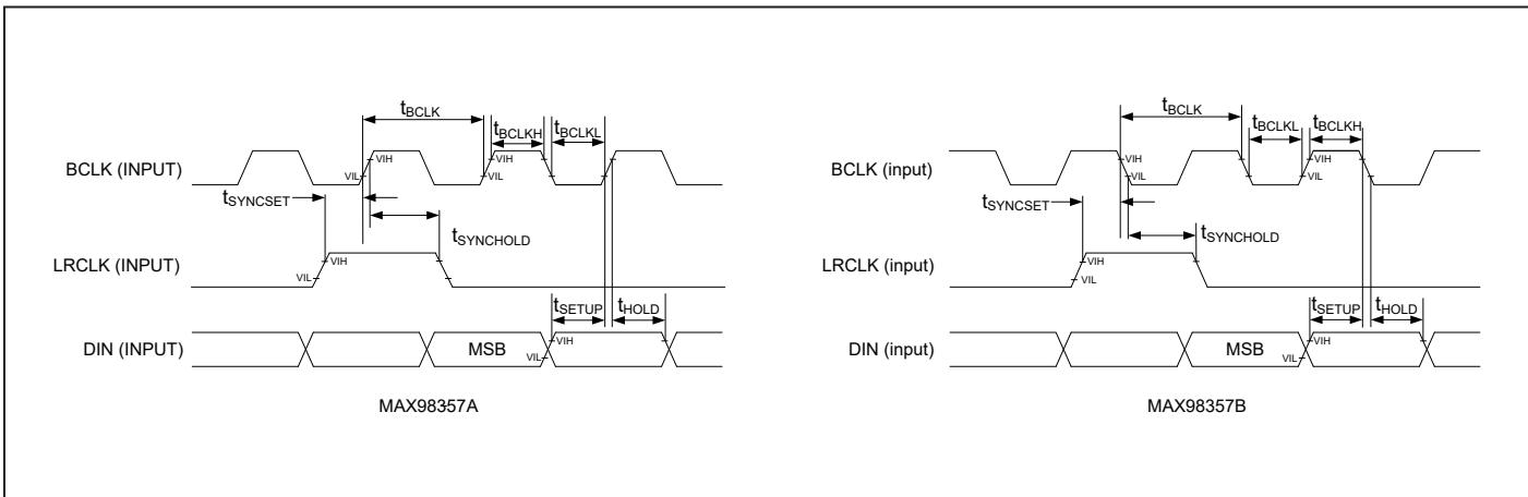
Figure 3. TDM Audio Interface Timing Diagram
Tiny, Low-Cost, PCM Class D Amplifier with Class AB Performance
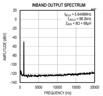
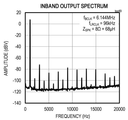
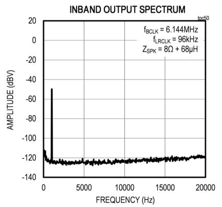
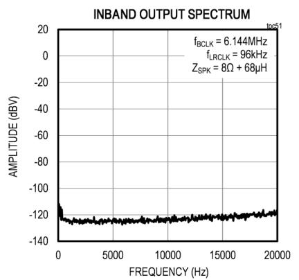
Typical Operating Characteristics
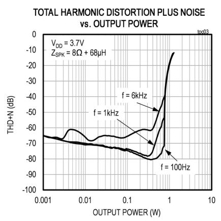
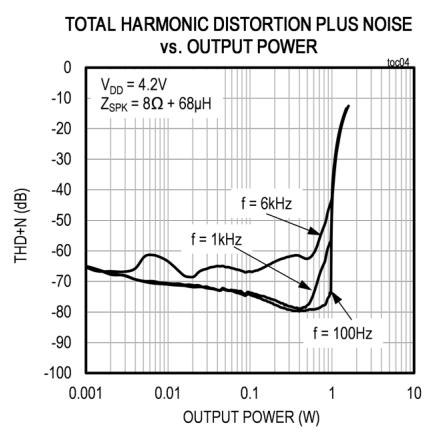
$( \mathsf { V } _ { \mathsf { D D } } = 5 \mathsf { V } , \mathsf { V } _ { \mathsf { G N D } } = 0 \mathsf { V } ,$ GAIN_SLOT = GND (+12dB). BCLK = 3.072MHz, LRCLK = 48kHz, speaker loads (ZSPK) connected between OUTP and OUTN, ${ \sf T } _ { \sf A } = { \sf T } _ { \sf M I N } { \sf t o } { \sf T } _ { \sf M A X } ,$ unless otherwise noted. Typical values are at $\bar { \mathsf { T } } _ { \mathsf { A } } = + 2 \bar { 5 } ^ { \circ } { \mathsf { C } } . )$


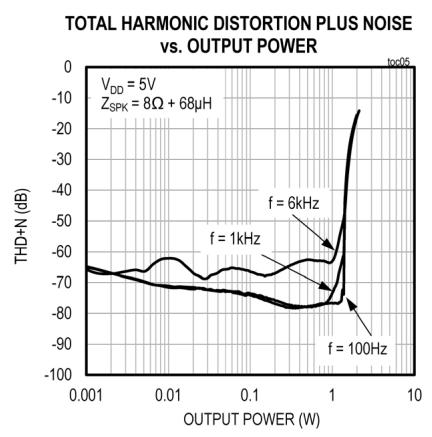


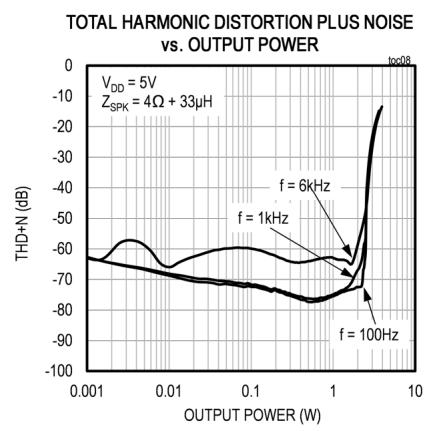
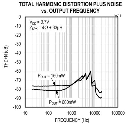
TOTAL HARMONIC DISTORTION PLUS NOISE vs. OUTPUT FREQUENCY
TOTAL HARMONIC DISTORTION PLUS NOISE vs. OUTPUT FREQUENCY
Tiny, Low-Cost, PCM Class D Amplifier with Class AB Performance
Typical Operating Characteristics (continued)
$( \mathsf { V } _ { \mathsf { D D } } = 5 \mathsf { V } , \mathsf { V } _ { \mathsf { G N D } } = 0 \mathsf { V } ,$ GAIN_SLOT = GND (+12dB). BCLK = 3.072MHz, LRCLK = 48kHz, speaker loads (ZSPK) connected between OUTP and OUTN, ${ \sf T } _ { \sf A } = { \sf T } _ { \sf M I N } { \sf t o } { \sf T } _ { \sf M A X } ,$ unless otherwise noted. Typical values are at $\mathsf { T } _ { \mathsf { A } } = + 2 5 ^ { \circ } \mathsf { C } .$ )
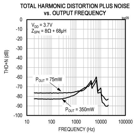

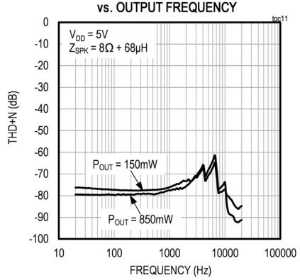


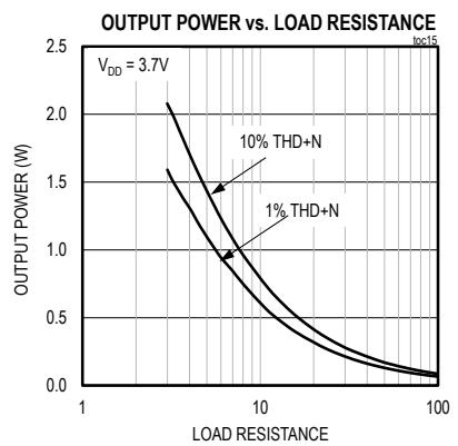
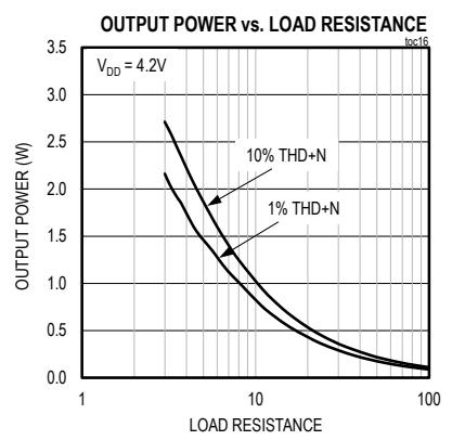

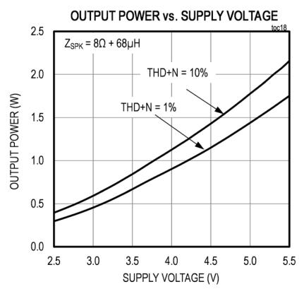
Tiny, Low-Cost, PCM Class D Amplifier with Class AB Performance
Typical Operating Characteristics (continued)
$( \mathsf { V } _ { \mathsf { D D } } = 5 \mathsf { V } , \mathsf { V } _ { \mathsf { G N D } } = 0 \mathsf { V } ,$ GAIN_SLOT = GND (+12dB). BCLK = 3.072MHz, LRCLK = 48kHz, speaker loads (ZSPK) connected between OUTP and OUTN, ${ \sf T } _ { \sf A } = { \sf T } _ { \sf M I N } { \sf t o } { \sf T } _ { \sf M A X } ,$ unless otherwise noted. Typical values are at $\mathsf { T } _ { \mathsf { A } } = + 2 5 ^ { \circ } \mathsf { C } .$ )


Tiny, Low-Cost, PCM Class D Amplifier with Class AB Performance
Typical Operating Characteristics (continued)
$( \mathsf { V } _ { \mathsf { D D } } = 5 \mathsf { V } , \mathsf { V } _ { \mathsf { G N D } } = 0 \mathsf { V } ,$ GAIN_SLOT = GND (+12dB). BCLK = 3.072MHz, LRCLK = 48kHz, speaker loads (ZSPK) connected between OUTP and OUTN, ${ \sf T } _ { \sf A } = { \sf T } _ { \sf M I N } { \sf t o } { \sf T } _ { \sf M A X } ,$ unless otherwise noted. Typical values are at $\mathsf { T } _ { \mathsf { A } } = + 2 5 ^ { \circ } \mathsf { C } .$ )





Tiny, Low-Cost, PCM Class D Amplifier with Class AB Performance
Typical Operating Characteristics (continued)
$( \mathsf { V } _ { \mathsf { D D } } = 5 \mathsf { V } , \mathsf { V } _ { \mathsf { G N D } } = 0 \mathsf { V } ,$ GAIN_SLOT = GND (+12dB). BCLK = 3.072MHz, LRCLK = 48kHz, speaker loads (ZSPK) connected between OUTP and OUTN, ${ \sf T } _ { \sf A } = { \sf T } _ { \sf M I N } { \sf t o } { \sf T } _ { \sf M A X } ,$ unless otherwise noted. Typical values are at $\mathsf { T } _ { \mathsf { A } } = + 2 5 ^ { \circ } \mathsf { C } .$ )




Tiny, Low-Cost, PCM Class D Amplifier with Class AB Performance
Typical Operating Characteristics (continued)
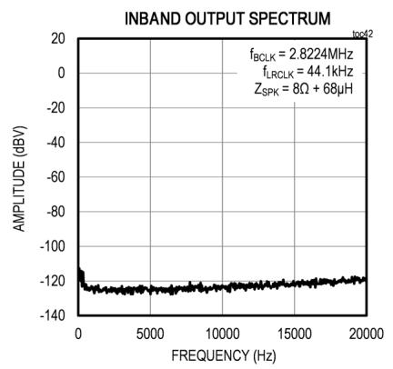
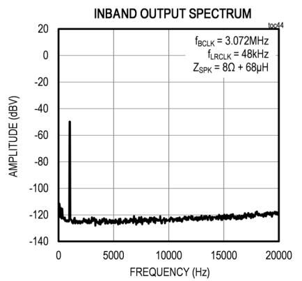
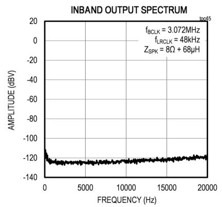
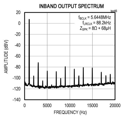
$( \mathsf { V } _ { \mathsf { D D } } = 5 \mathsf { V } , \mathsf { V } _ { \mathsf { G N D } } = 0 \mathsf { V } ,$ GAIN_SLOT = GND (+12dB). BCLK = 3.072MHz, LRCLK = 48kHz, speaker loads (ZSPK) connected between OUTP and OUTN, ${ \sf T } _ { \sf A } = { \sf T } _ { \sf M I N } { \sf t o } { \sf T } _ { \sf M A X } ,$ unless otherwise noted. Typical values are at $\bar { \mathsf { T } } _ { \mathsf { A } } = + 2 \bar { 5 } ^ { \circ } { \mathsf { C } } . )$


Pin Configurations
WLP

Pin Description
| PIN | NAME | FUNCTION | |
| WLP | TQFN | ||
| A1 | 4 | SD_MODE | Shutdown and Channel Select. Pull SD_MODE low to place the device in shutdown. In I2S or LJ mode, SD_MODE selects the data channel (Table 5). In TDM mode, SD_MODE and GAIN_SLOT are both used for channel selection (Table 7). |
| A2 | 7,8 | V_DD | Power-Supply Input |
| A3 | 9 | OUTP | Positive Speaker Amplifier Output |
| B1 | 1 | DIN | Digital Input Signal |
| B2 | 2 | GAIN_SLOT | Gain and Channel Selection. In I2S and LJ mode determines amplifier output gain (Table 8) In TDM mode, used for channel selection with SD_MODE (Table 7). In TDM mode, gain is fixed at 12dB. |
| B3 | 10 | OUTN | Negative Speaker Amplifier Output |
| C1 | 16 | BCLK | Bit Clock Input |
| C2 | 3,11,15 | GND | Ground |
| C3 | 14 | LRCLK | Frame Clock. Left/right clock for I2S and LJ mode. Sync clock for TDM mode. |
| — | 5,6,12,13 | N.C. | No Connection |
| — | — | EP | Exposed Pad. The exposed pad is not internally connected. Connect the exposed page to a solid ground plane for thermal dissipation. |
Tiny, Low-Cost, PCM Class D Amplifier with Class AB Performance
Detailed Description
The MAX98357A/MAX98357B are digital PCM input Class D power amplifiers. The MAX98357A accepts standard I2S data through DIN, BCLK, and LRCLK while the MAX98357B accepts left-justified data through the same inputs. Both versions also accept 16-bit or 32-bit TDM data with up to eight slots. The digital audio interface eliminates the need for an external MCLK signal that is typically required for I2S data transmission.
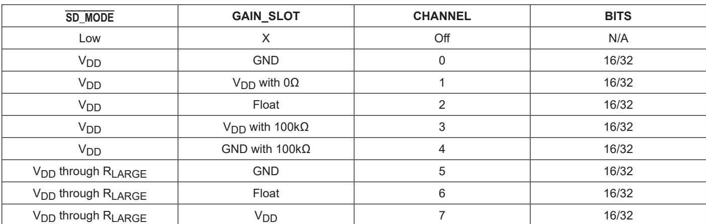
SD_MODE selects which data word is output by the amplifier and is used to put the ICs into shutdown. These devices offer five gain settings in I2S/left-justified mode and a fixed 12dB gain in TDM mode. Channel selection in TDM mode is set with the combination of SD_MODE and GAIN_SLOT (Table 7).
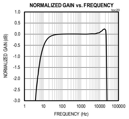
The MAX98357A/MAX98357B DAI includes a DC blocker with a -3dB cutoff at 3.7Hz.
The MAX98357A/MAX98357B feature low-quiescent current, comprehensive click-and-pop suppression, and excellent RF immunity. The ICs offer Class AB audio performance with Class D efficiency in a minimal boardspace solution. The Class D amplifier features spreadspectrum modulation with edge-rate and overshoot control circuitry that offers significant improvements in switchmode amplifier radiated emissions. The amplifier features click-and-pop suppression that reduces audible transients on startup and shutdown. The amplifier includes thermaloverload and short-circuit protection.
Digital Audio Interface Modes
The input stage of the digital audio interface is highly flexible, supporting 8kHz–96kHz sampling rates with 16/24/32- bit resolution for I2S/left justified data as well as up to a 8-slot, 16-bit or 32-bit time division multiplexed (TDM) format. When LRCLK has a 50% duty cycle the data format is determined by the part number selection (MAX98357A/MAX98357B). When a frame sync pulse is used for the LRCLK the data format is automatically configured in TDM mode. The frame sync pulse indicates the beginning of the first time slot.
MCLK Elimination
The ICs eliminate the need for the external MCLK signal that is typically used for PCM communication. This reduces EMI and possible board coupling issues in addition to reducing the size and pin-count of the ICs.
BCLK Jitter Tolerance
The ICs feature a BCLK jitter tolerance of 0.5ns for RMS jitter below 40kHz and 12ns for wideband RMS jitter while maintaining a dynamic range greater than 98dB (Table 1).
BCLK Polarity
When operating in I2S/left-justified mode, incoming serial data is always clocked-in on the rising edge of BCLK. In TDM mode, the MAX98357A clocks-in serial data on the rising edge of BCLK while the MAX98357B clocks in serial data on the falling edge of BCLK (Table 2).
LRCLK Polarity
LRCLK specifies whether left-channel data or rightchannel data is currently being read by the digital audio interface. The MAX98357A indicates the left channel word when LRCLK is low, and the MAX98357B indicates the left channel word when LRCLK is high (Table 3).
LRCLK ONLY supports 8kHz, 16kHz, 32kHz, 44.1kHz, 48kHz, 88.2kHz and 96kHz frequencies. LRCLK clocks at 11.025kHz, 12kHz, 22.05kHz and 24kHz are NOT supported. Do not remove LRCLK while BCLK is present. Removing LRCLK while BCLK is present can cause unexpected output behavior including a large DC output voltage.
Standby Mode
The ICs automatically enter standby mode when BCLK is removed. If BCLK stops toggling, the ICs automatically
Table 1. RMS Jitter Tolerance
| FREQUENCY | RMS JITTER TOLERANCE (ns) |
| < 40kHz | 0.5 |
| 40kHz–BCLK | 12 |
Table 2. BCLK Polarity
| MODE | PART NUMBER | BCLK POLARITY |
| $I^{2}S$ | MAX98357A | Rising edge |
| Left-justified | MAX98357B | Rising edge |
| TDM | MAX98357A | Rising edge |
| MAX98357B | Falling edge |
Table 3. LRCLK Polarity
| PART NUMBER | LRCLK POLARITY (LEFT CHANNEL) |
| MAX98357A | Low |
| MAX98357B | High |
Tiny, Low-Cost, PCM Class D Amplifier with Class AB Performance
enter standby mode. In standby mode, the Class D speaker is turned off and the outputs go into a high-impedance state, ensuring that unwanted current is not transferred to the load during this condition. Standby mode has reduced power consumption from normal operation (340µA), but does not reach as low as full shutdown (0.6µA). Standby mode can be used to reduce power consumption when no GPIO us available to pull SD_MODE low.
DAC Digital Filters
The DAC features a digital lowpass filter that is automatically configured for voice playback or music playback based on the sample rate that is used. This filter eliminates the effect of aliasing and any other high-frequency noise that might otherwise be present. Table 4 shows the digital filter settings that are automatically selected.
SD_MODE and Shutdown Operation
The ICs feature a low-power shutdown mode, drawing less than 0.6µA (typ) of supply current. During shutdown, all internal blocks are turned off, including setting the output stage to a high-impedance state. Drive SD_MODE low to put the ICs into shutdown.
The state of SD_MODE determines the audio channel that is sent to the amplifier output (Table 5).
Drive SD_MODE high to select the left word of the stereo input data. Drive SD_MODE high through a sufficiently small resistor to select the right word of the stereo input data. Drive SD_MODE high through a sufficiently large resistor to select both the left and right words of the stereo input data (left/2 + right/2). RLARGE and RSMALL are determined by the VDDIO voltage (logic voltage from control interface) that is driving SD_MODE according to the following two equations:
$$
R _ {S M A L L} (k \Omega) = 9 4. 0 \times V _ {D D I O} - 1 0 0
$$
$$
R _ {L A R G E} (k \Omega) = 2 2 2. 2 \times V _ {D D I O} - 1 0 0
$$
When the devices are configured in left-channel mode (SD_MODE is directly driven to logic-high by the control interface), take care to avoid violating the Absolute Maximum Ratings limits for SD_MODE. Ensuring that VDD is always greater than VDDIO is one way to prevent SD_MODE from violating the Absolute Maximum Ratings limits. If this is not possible in the application (e.g., if VDD < 3.0V and $\mathsf { V } _ { \mathsf { D D I O } } = 3 . 3 \mathsf { V } )$ , then it is necessary to add a small resistance (~2kΩ) in series with SD_MODE to limit the current into the SD_MODE pin. This is not a concern when using the right channel or (left/2 + right/2) modes.
Figure 4 and Figure 5 show how to connect an external resistor to SD_MODE when using an open-drain driver or a push-pull driver.
Table 4. Digital Filter Settings
| LRCLK FREQUENCY | -3dB CUTOFF FREQUENCY | RIPPLE LIMIT CUTOFF FREQUENCY | STOPBAND CUTOFF FREQUENCY | STOPBAND ATTENUATION (dB) |
| $f_{LRCLK} < 30kHz$ | $0.446 \times f_{LRCLK}$ | $0.443 \times f_{LRCLK}$ | $0.464 \times f_{LRCLK}$ | 75 |
| $30kHz < f_{LRCLK} < 50kHz$ | $0.47 \times f_{LRCLK}$ | $0.43 \times f_{LRCLK}$ | $0.58 \times f_{LRCLK}$ | 60 |
| $f_{LRCLK} > 50kHz$ | $0.31 \times f_{LRCLK}$ | $0.24 \times f_{LRCLK}$ | $0.477 \times f_{LRCLK}$ | 60 |
Table 5. SD_MODE Control
| SD_MODE STATUS | SELECTED CHANNEL | |
| High | $V_{SD\_MODE} > B2$ trip point | Left |
| Pullup through $R_{SMALL}$ | B2 trip point $> V_{SD\_MODE} > B1$ trip point | Right |
| Pullup through $R_{LARGE}$ | B1 trip point $> V_{SD\_MODE} > B0$ trip point | (Left/2 + right/2) |
| Low | B0 trip point $> V_{SD\_MODE}$ | Shutdown |
Table 6. Examples of SD_MODE Pullup Resistor Values
| LOGIC VOLTAGE LEVEL (VDDIO) (V) | RSMALL (kΩ) | RLARGE (kΩ) |
| 1.8 | 69.8 | 300 |
| 3.3 | 210.2 | 634 |
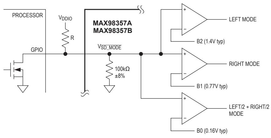
Figure 4. SD_MODE Resistor Connected Using Open-Drain Driver
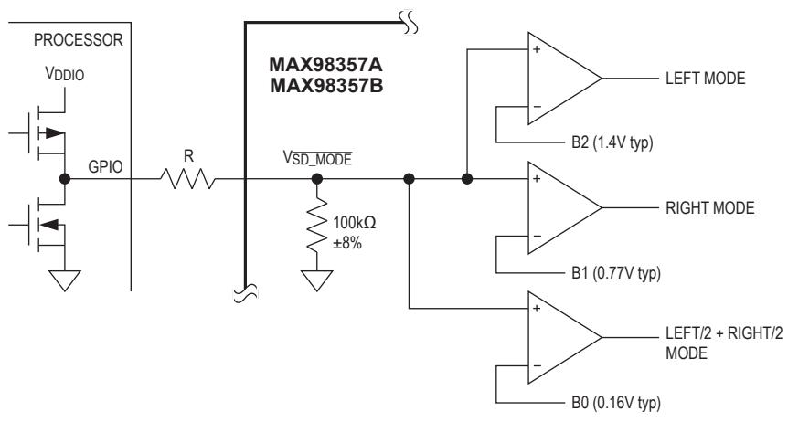
Figure 5. SD_MODE Resistor Connected Using Push-Pull Driver
Startup
With the exception of BCLK = 256KHz, the only required sequence for startup is that LRCLK must start within 1/2 LRCLK period of BCLK starting.
When using a mode with BCLK = 256kHz, there are additional requirements for the part to power-up properly:
BCLK and LRCLK cannot be applied before the part is enabled.
BCLK and LRCLK must start from logic low and transition to logic high.
After VDD is > 2.3V AND SD_MODE is high, there must be a 10μs wait time before starting BCLK and LRCLK.
LRCLK must start at least 1/2 BCLK after BCLK starts.
LRCLK must start no more than 1/2 LRCLK after BCLK starts.
LRCLK must complete a full cycle; no partial LRCLK cycles.
Once started, BCLK and LRCLK must remain switching at 256kHz and 8kHz, respectively, and cannot be interrupted during device operation. If BCLK and LRCLK need to be stopped, SD_MODE must first be set to 0V. Subsequent startups with BCLK = 256kHz and LRCLK = 8kHz need to follow the sequence described in steps 1-6.
Figure 6 shows an example where VDD reaches UVLO maximum before SD_MODE is applied. In this example, the 10μs wait time starts after SD_MODE is applied.

Figure 6. Required startup sequence when using BCLK = 256kHz
I2S and Left Justified Mode
The MAX98357A follows standard I2S timing by allowing a delay of one BCLK cycle after the LRCLK transition before the beginning of a new data word (Figure 7 and Figure 8). The MAX98357B follows the left justified timing specification by aligning the LRCLK transitions with the beginning of a new data word (Figure 9 and Figure 10). LRCLK ONLY supports 8kHz, 16kHz, 32kHz, 44.1kHz, 48kHz, 88.2kHz, and 96kHz frequencies. LRCLK clocks at 11.025kHz, 12kHz, 22.05kHz and 24kHz are NOT supported. Do not remove LRCLK while BLCK is present. Removing LRCLK while BCLK is present can cause unexpected output behavior, including a large DC output voltage.
The digital audio interface output mode is chosen by the voltage at SD_MODE. Table 5 shows how the available modes are selected. Trip point B0–B2 are shown the Electrical Characteristics in the SD_MODE Comparator Trip Points section. Values for SD_MODE pullup resistors
RSMALL and RLARGE are dependent on the voltage level of VDDIO. See Table 6 for pullup resistor values.
TDM Mode
TDM mode is automatically detected by monitoring the short channel sync pulse on LRCLK. The frequency detector circuit detects the bit depth. In TDM mode, the MAX98357A/MAX98357B has a fixed gain of 12dB. GAIN_SLOT and SD_MODE are used to select to which of 8 channels of TDM data the parts respond. Table 7 shows the connections for GAIN_SLOT and SD_MODE for channel selection. The MAX98357A data is valid on the BCLK rising edge. The MAX98357B data is valid on the BCLK falling edge.
Figure 11, Figure 12, Figure 13, and Figure 14 show TDM operation, in which a frame-sync pulse is used for LRCLK. In TDM mode, there must be 128 (16-bit mode) or 256 (32-bit mode) BCLK cycles per frame. In TDM mode, the ICs only accept 16-bit or 32-bit formatted data and any of the 8 TDM slots can be selected.
Table 7. TDM Mode Channel Selection
| SD_MODE | GAIN_SLOT | CHANNEL | BITS |
| Low | X | Off | N/A |
| $V_{DD}$ | GND | 0 | 16/32 |
| $V_{DD}$ | $V_{DD}$ with 0Ω | 1 | 16/32 |
| $V_{DD}$ | Float | 2 | 16/32 |
| $V_{DD}$ | $V_{DD}$ with 100kΩ | 3 | 16/32 |
| $V_{DD}$ | GND with 100kΩ | 4 | 16/32 |
| $V_{DD}$ through $R_{LARGE}$ | GND | 5 | 16/32 |
| $V_{DD}$ through $R_{LARGE}$ | Float | 6 | 16/32 |
| $V_{DD}$ through $R_{LARGE}$ | $V_{DD}$ | 7 | 16/32 |

Figure 7. MAX98357A I2S Digital Audio Interface Timing, 16-Bit Resolution
D31D30D29D28D27D26D25D24D23D22D21D20D19D18D17D16D15D14D13D12D11D10D9D8D7D6D5D4D3D2D1D0D31D30D29D28D27D26D25D24D23D22D21D20D19D18D17D16D15D14D13D12D11D10D9D8D7D6D5D4D3D2D1D0D31D30DIN BCLK
Figure 8. MAX98357A I2S Digital Audio Interface Timing, 32-Bit Resolution
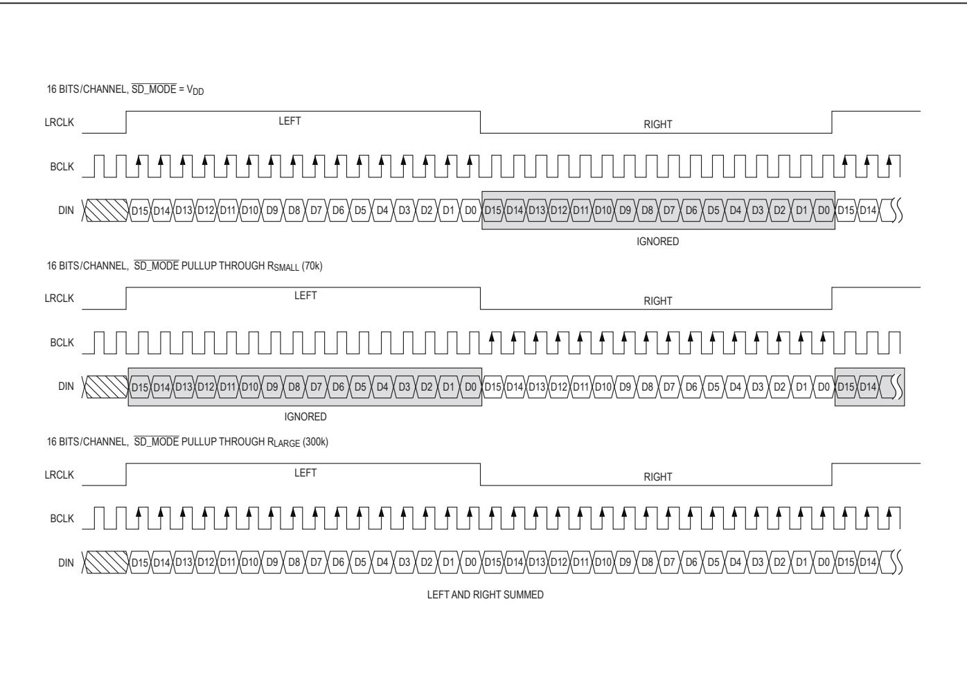
Figure 9. MAX98357B Left-Justified Digital Audio Interface Timing, 16-Bit Resolution
Figure 10. MAX98357B Left-Justified Digital Audio Interface Timing, 32-Bit Resolution
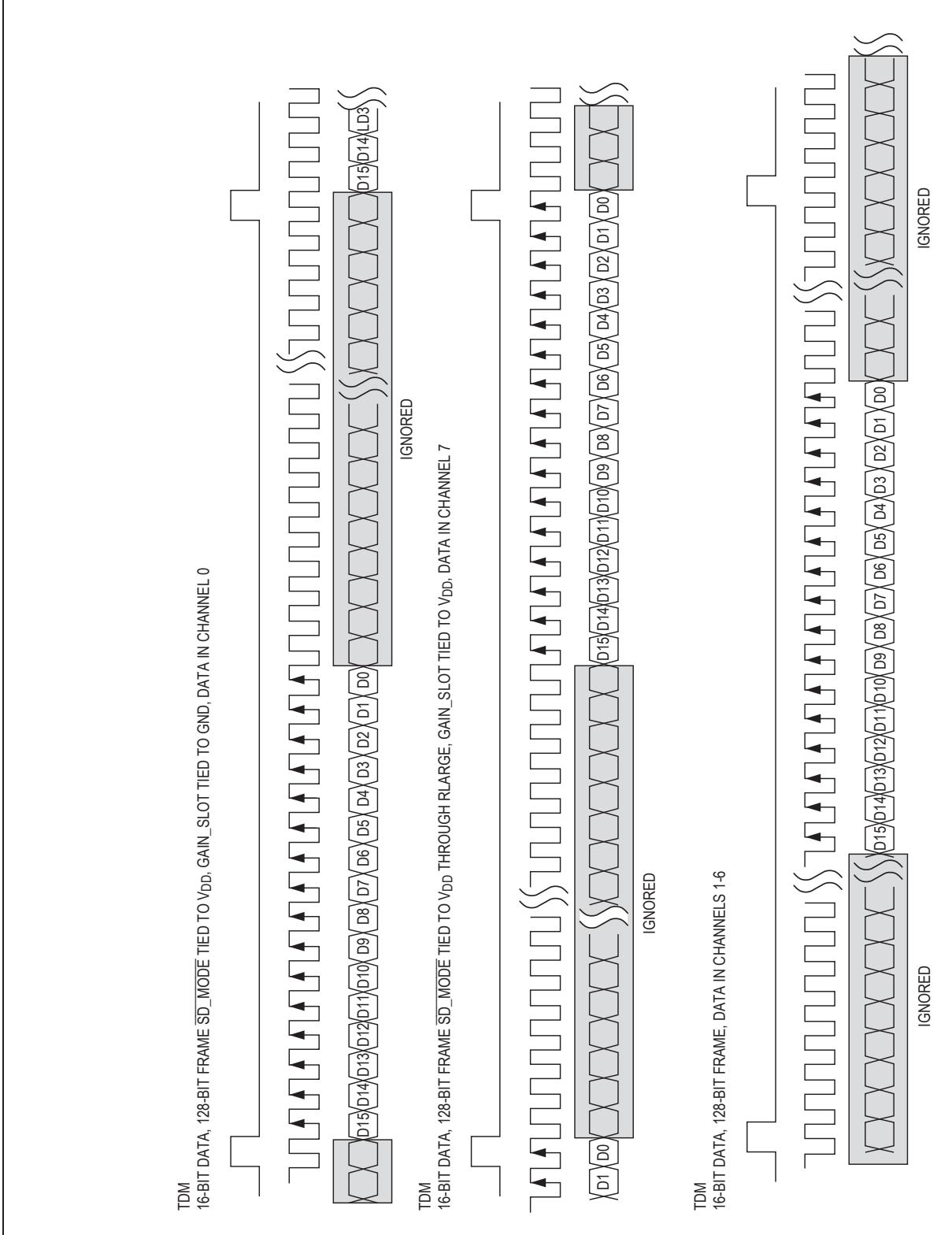
Figure 11. MAX98357A TDM 16-Bit DAI Timing
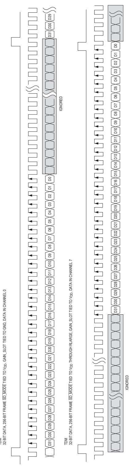
DM 32-BITDATA,256-BITFRAMESD_MODETIEDTOVDD,GAIN_SLOTTIEDTOGND,DATAINCHANNEL 0
Figure 12. MAX98357A TDM 32-Bit DAI Timing
DM 32-BITDATA,256-BITFRAMESD_MODETIEDTOVDDTHROUGHRLARGE,GAIN_SLOTTIEDTOVDD,DATAINCHANNEL 7
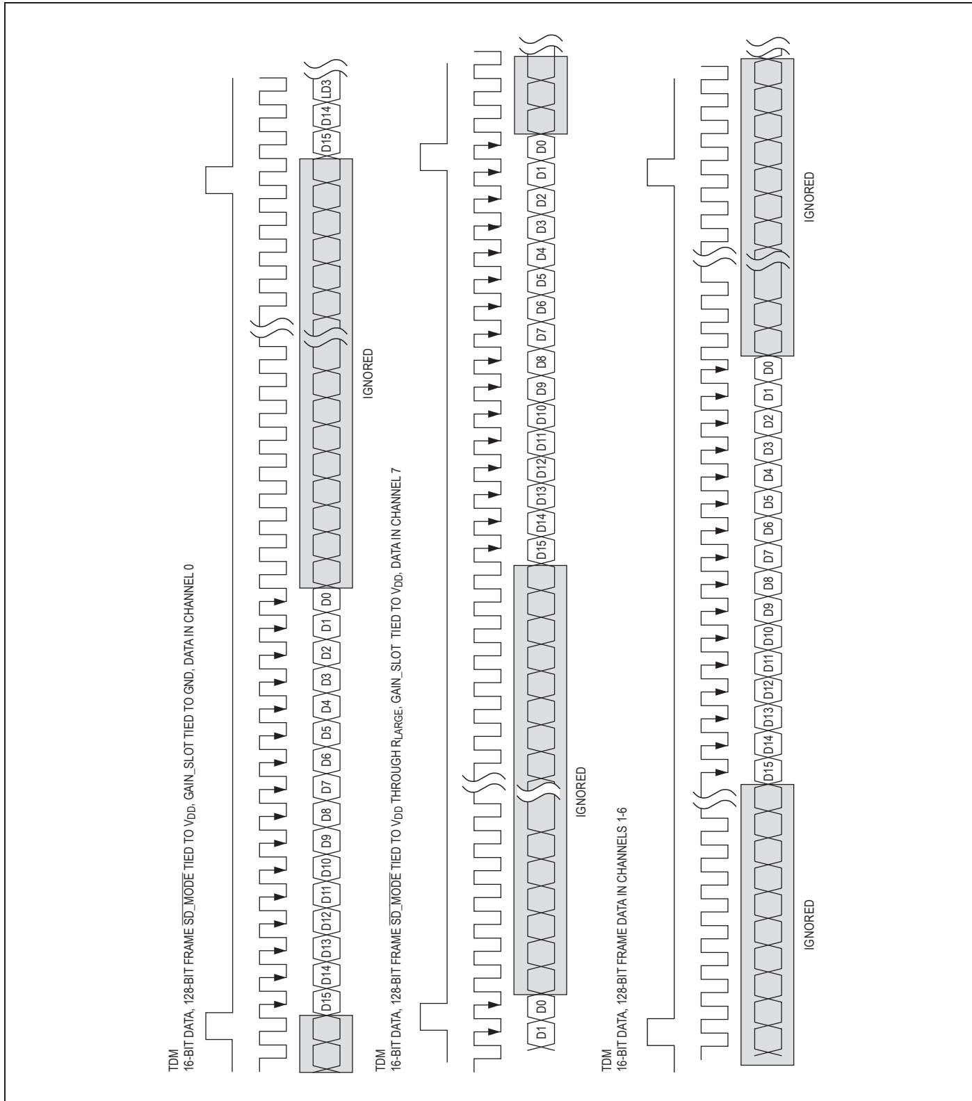
Figure 13. MAX98357B TDM 16-Bit DAI Timing
TDM 32-BIT DATA, 256-BIT FRAME SD_MODE TIED TO VDD, GAIN_SLOT TIED TO GND, DATA IN CHANNEL 0
Figure 14. MAX98357B TDM 32-Bit DAI Timing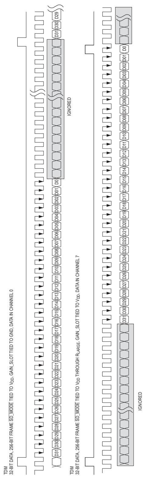
Tiny, Low-Cost, PCM Class D Amplifier with Class AB Performance
Class D Speaker Amplifier
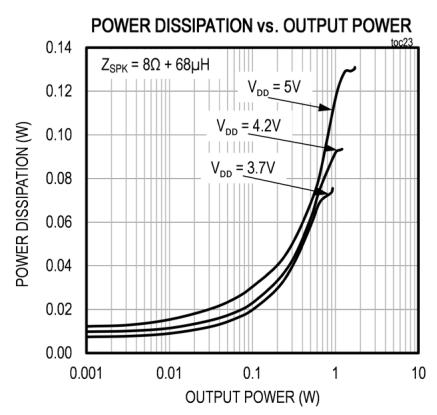
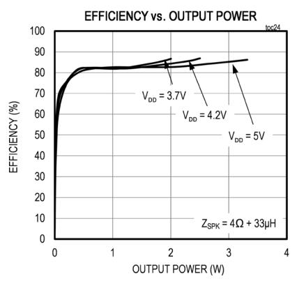
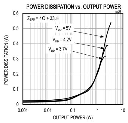
The filterless Class D amplifier offers much higher efficiency than Class AB amplifiers. The high efficiency of a Class D amplifier is due to the switching operation of the output stage transistors. Any power loss associated with the Class D output stage is mostly due to the I2R loss of the MOSFET on-resistance and quiescent current overhead.
Ultra-Low EMI Filterless Output Stage
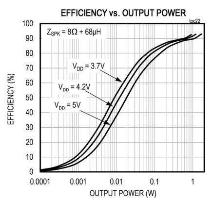
Traditional Class D amplifiers require the use of externa LC filters, or shielding, to meet EN55022B electromagnetic-interference (EMI) regulation standards. Maxim’s active emissions-limiting edge-rate control circuitry and spreadspectrum modulation reduces EMI emissions while maintaining up to 92% efficiency.
Maxim’s spread-spectrum modulation mode flattens wideband spectral components while proprietary techniques ensure that the cycle-to-cycle variation of the switching period does not degrade audio reproduction or efficiency. The ICs’ spread-spectrum modulator randomly varies the switching frequency by ±20kHz around the center frequency (300kHz). Above 10MHz, the wideband spectrum looks like noise for EMI purposes (Figure 15).
Speaker Current Limit
If the output current of the speaker amplifier exceeds the current limit (2.8A typ), the IC disables the outputs for approximately 100µs. At the end of the 100µs, the outputs are re-enabled. If the fault condition still exists, the IC continues to disable and reenable the outputs until the fault condition is removed.
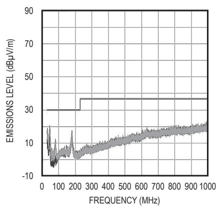
Figure 15. EMI with 12in of Speaker Cable and No Output Filtering
Gain Selection
The ICs offer five programmable gain selections through a single gain input (GAIN_SLOT) in I2S/left justified mode. Gain is referenced to the full-scale output of the DAC, which is 2.1dBV (Table 8). In TDM mode, the gain is automatically set at a fixed 12dB. Assuming that the desired output swing is not limited by the supply voltage rail, the IC’s output level can be calculated based on the digital input signal level and selected amplifier gain according to the following equation:
Output signal level (dBV) = input signal level (dBFS) + 2.1dB + selected amplifier gain (dB)
where 0dBFS is referenced to 0dBV.
Click-and-Pop Suppression
The IC speaker amplifier features Maxim’s comprehensive click-and-pop suppression. During startup, the clickand-pop suppression circuitry reduces audible transient sources internal to the device by ramping the input signal from mute to 0dB. When entering shutdown, the differential speaker outputs simultaneously drop to GND.
The comprehensive click-and-pop suppression of the MAX98357 is unaffected by power-up or power-down sequencing. Applying the DAI clocks before or after the transition of SD_MODE yields the same click-and-pop performance. The MAX98357 does not have a volume ramp-down response when entering shutdown. For optimal click-and-pop performance, ramp down the digital data on SDIN before powering down the MAX98357.
Table 8. Gain Selection
| GAIN_SLOT | I2S/LJ GAIN (dB) |
| Connect to GND through 100kΩ ±5% resistor | 15 |
| Connect to GND | 12 |
| Unconnected | 9 |
| Connect to VDD | 6 |
| Connect to VDD through 100kΩ ±5% resistor | 3 |
Applications Information
Figure 16. Left-Channel PCM Operation with 6dB Gain
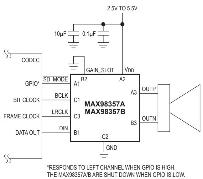
Figure 17. Left-Channel PCM Operation with 12dB Gain

Figure 18. Right-Channel PCM Operation with 6dB Gain
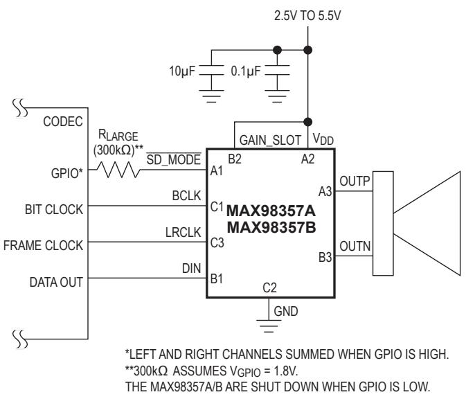
Figure 19. (Left/2 + Right/2) PCM Operation with 6dB Gain

Figure 20. Stereo PCM Operation Using Two ICs
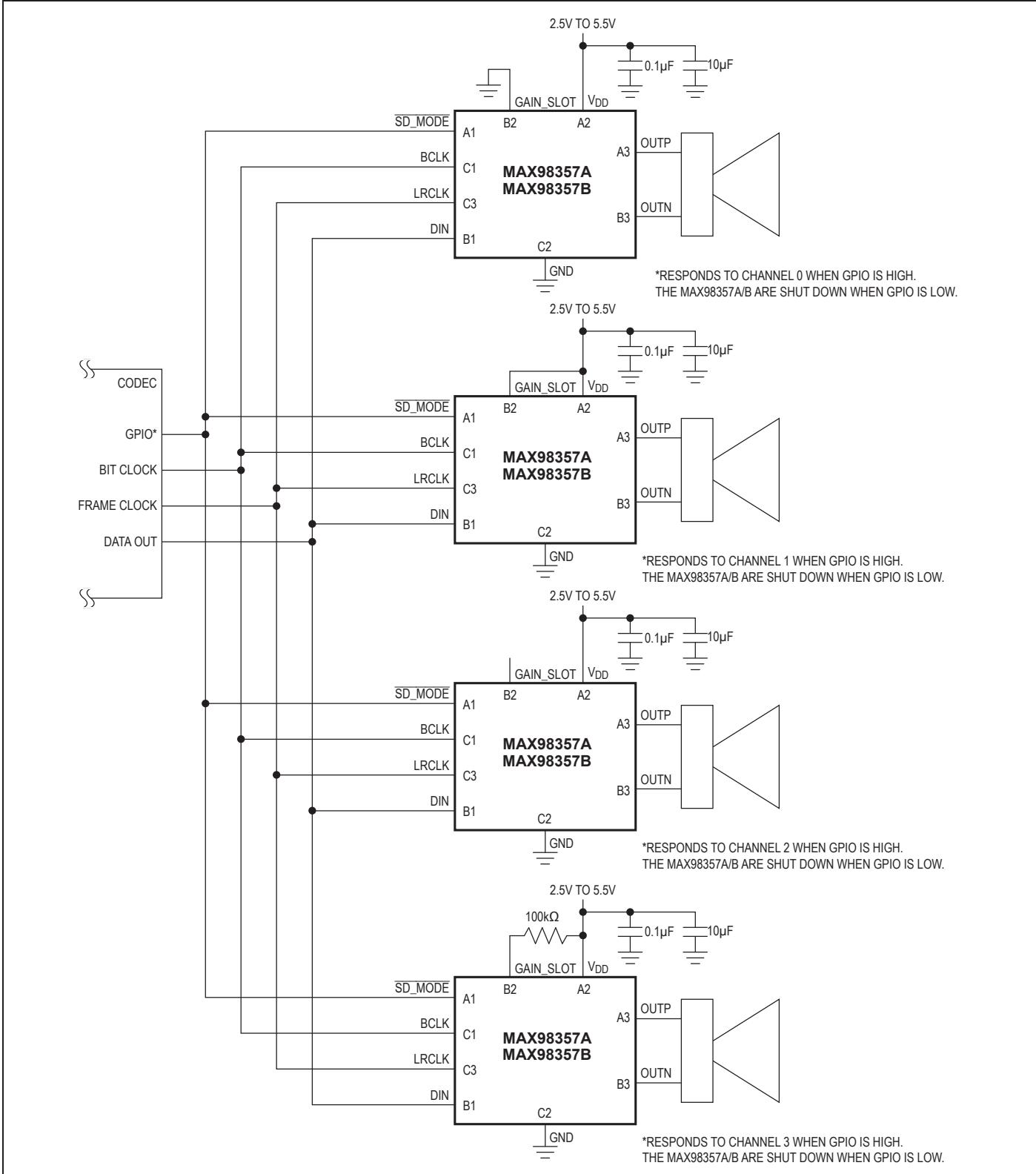
Figure 21. Channel TDM Operation (Gain Fixed at 12dB)
Functional Diagram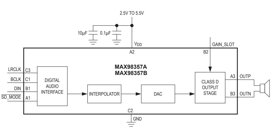
Filterless Class D Operation
Traditional Class D amplifiers require an output filter to recover the audio signal from the amplifier’s output. The filter adds cost, size, and decreases efficiency and THD+N performance. The ICs’ filterless modulation scheme does not require an output filter. The device relies on the inherent inductance of the speaker coil and the natural filtering of both the speaker and the human ear to recover the audio component of the square-wave output.
Because the switching frequency of the ICs is well beyond the bandwidth of most speakers, voice coil movement due to the switching frequency is very small. Use a speaker with a series inductance > 10µH. Typical 8Ω speakers exhibit series inductances in the 20µH to 100µH range.
Power-Supply Input
VDD, which ranges from 2.5V to 5.5V, powers the IC, including the speaker amplifier. Bypass VDD with a 0.1µF and 10µF capacitor to GND. Some applications might require only the 10µF bypass capacitor, making it possible to operate with a single external component. Apply additional bulk capacitance at the ICs if long input traces between VDD and the power source are used.
Layout and Grounding
Proper layout and grounding are essential for optimum performance. Good grounding improves audio performance and prevents switching noise from coupling into the audio signal.
Use wide, low-resistance output traces. As load impedance decreases, the current drawn from the device outputs increases. At higher current, the resistance of the output traces decreases the power delivered to the load. For example, if 2W is delivered from the speaker output to a 4Ω load through 100mΩ of total speaker trace, 1.904W is being delivered to the speaker. If power is delivered through 10mΩ of total speaker trace, 1.951W is being delivered to the speaker. Wide output, supply, and ground traces also improve the power dissipation of the ICs. Parasitic capacitance on the output traces cause higher quiescent current by VDD x 300kHz x CPARASITIC.
For example, at VDD = 5V and a total parasitic capacitance of 100pF (50pF on each output trace), the increase in quiescent current is 5 x 300kHz x 100pF = 150µA.
The ICs are inherently designed for excellent RF immunity. For best performance, add ground fills around all signal traces on top or bottom PCB planes.
Tiny, Low-Cost, PCM Class D Amplifier with Class AB Performance
MAX98357A/ MAX98357B
Gains of 6dB, 9dB, and 12dB are selectable without using a via or routing out the center bump of the WLP. This simplifies the layout and allows for inexpensive PCB fabrication. Here is a layout example with the gain set to 12dB. The center bump is tied to the adjacent GND pin. Refer to Application Note 6643: Optimize Cost, Size, and Performance with MAX98357 WLP for more information.

Figure 22. WLP Pin Connect for set 12dB Gain Without Via.
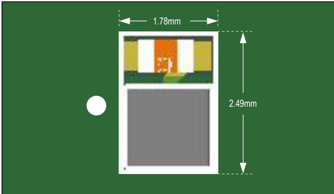
Figure 23. Example Layout Configured for Left-Channel Audio and Gain of 12dB.
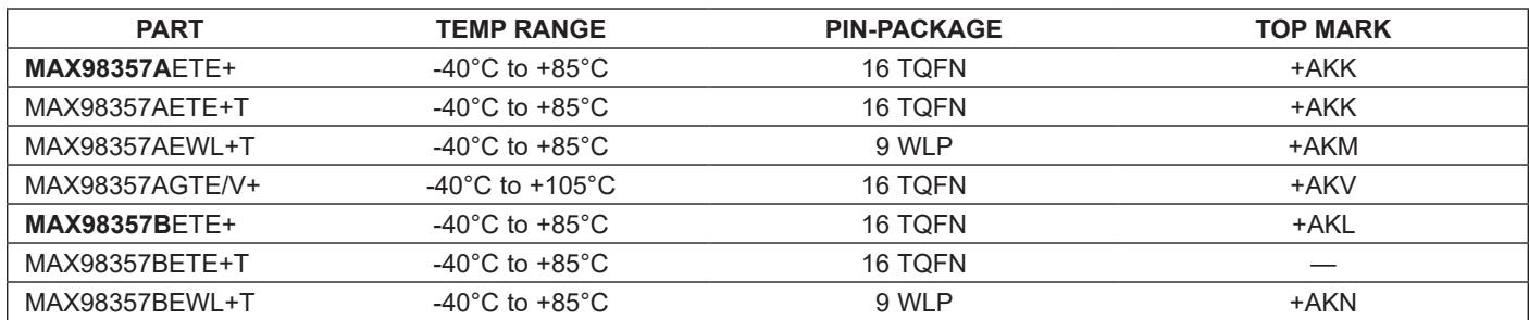
Ordering Information
In many applications, the only passive component required would be a single capacitor which results in a tiny solution size of 4.32mm2.
WLP Applications Information
For the latest application details on WLP construction, dimensions, tape carrier information, PCB techniques, bump-pad layout, and recommended reflow temperature profile, as well as the latest information on reliability testing results, refer to the Application Note 1891: Wafer-Level Packaging (WLP) and Its Applications. Figure 24 shows the dimensions of the WLP balls used on the ICs.

Figure 24. MAX98357A/MAX98357B WLP Ball Dimensions
| PART | TEMP RANGE | PIN-PACKAGE | TOP MARK |
| MAX98357AETE+ | -40°C to +85°C | 16 TQFN | +AKK |
| MAX98357AETE+T | -40°C to +85°C | 16 TQFN | +AKK |
| MAX98357AEWL+T | -40°C to +85°C | 9 WLP | +AKM |
| MAX98357AGTE/V+ | -40°C to +105°C | 16 TQFN | +AKV |
| MAX98357BETE+ | -40°C to +85°C | 16 TQFN | +AKL |
| MAX98357BETE+T | -40°C to +85°C | 16 TQFN | — |
| MAX98357BEWL+T | -40°C to +85°C | 9 WLP | +AKN |
+Denotes a lead(Pb)-free/RoHS-compliant package.
T = Tape and reel.
/V denotes an automotive-qualified part.
Tiny, Low-Cost, PCM Class D Amplifier with Class AB Performance
Package Information
For the latest package outline information and land patterns (footprints), go to www.analog.com/packages. Note that a “+”, “#”, or “-” in the package code indicates RoHS status only. Package drawings may show a different suffix character, but the drawing pertains to the package regardless of RoHS status.
| PACKAGE TYPE | PACKAGE CODE | OUTLINE NO. | LAND PATTERN NO. |
| 9 WLP | W91F1+1 | 21-0896 | Refer toApplication Note 1891 |
| 16 TQFN | T1633+4 | 21-0136 | 90-0031 |

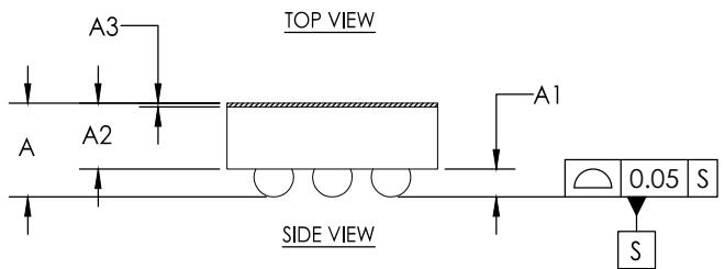


| COMMON DIMENSIONS | |
| A | 0.64±0.05 |
| A1 | 0.19±0.03 |
| A2 | 0.45 REF |
| A3 | 0.04 BASIC |
| b | ∅ 0.27±0.03 |
| D | 1.347 ±0.025 |
| D1 | 0.80 BASIC |
| E | 1.437 ±0.025 |
| E1 | 0.80 BASIC |
| e | 0.40 BASIC |
| SD | 0.00 BASIC |
| SE | 0.00 BASIC |
| DEPOPULATED BUMPS:NONE | |
FRONT VIEW
BOTTOM VIEW
NOTES:
Terminal pitch is defined by terminal center to center value
Outer dimension is defined by center lines between scribe lines.
All dimensions in millimeter.
Marking shown is for package orientation reference only
Tolerance is ± 0.02 unless specified otherwise.
All dimensions apply to PbFree (+) package codes only.
Front - side finish can be either Black or Clear.

| APPROVAL | DOCUMENT CONTROL NO.21-0896 | REV.B | $\frac{1}{1}$ |
Tiny, Low-Cost, PCM Class D Amplifier with Class AB Performance
Package Information (continued)
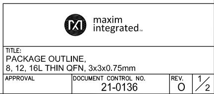
For the latest package outline information and land patterns (footprints), go to www.analog.com/packages. Note that a “+”, “#”, or “-” in the package code indicates RoHS status only. Package drawings may show a different suffix character, but the drawing pertains to the package regardless of RoHS status.

TOP VIEW

BOTTOM VIEW
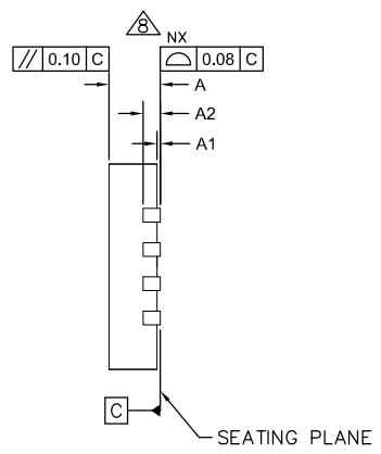
SIDE VIEW
-DRAWING NOT TO SCALE-
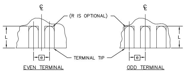
DETAIL A
Tiny, Low-Cost, PCM Class D Amplifier with Class AB Performance
Package Information (continued)
For the latest package outline information and land patterns (footprints), go to www.analog.com/packages. Note that a “+”, “#”, or “-” in the package code indicates RoHS status only. Package drawings may show a different suffix character, but the drawing pertains to the package regardless of RoHS status.
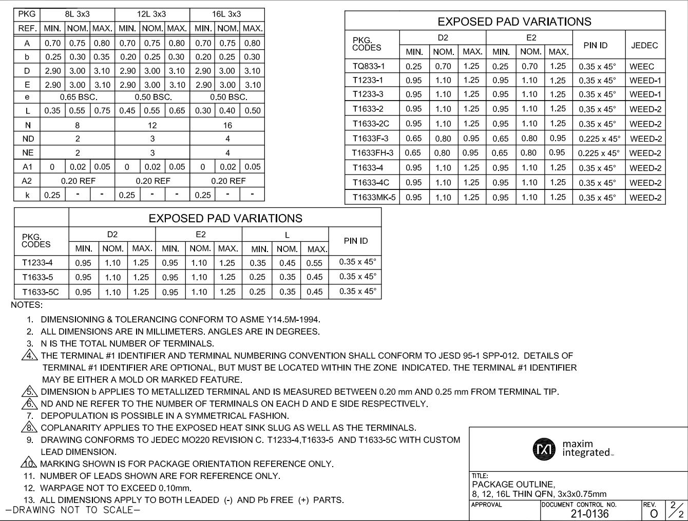
| PKG | 8L 3x3 | 12L 3x3 | 16L 3x3 | EXPOSED PAD VARIATIONS | |||||||||||||
| REF. | MIN. | NOM. | MAX. | MIN. | NOM. | MAX. | MIN. | NOM. | MAX. | PKG.CODES | D2 | E2 | PIN ID JEDEC | ||||
| A | 0.70 | 0.75 | 0.80 | 0.70 | 0.75 | 0.80 | 0.70 | 0.75 | 0.80 | MIN. | NOM. | MAX. | MIN. | NOM. | MAX. | ||
| b | 0.25 | 0.30 | 0.35 | 0.20 | 0.25 | 0.30 | 0.20 | 0.25 | 0.30 | ||||||||
| D | 2.90 | 3.00 | 3.10 | 2.90 | 3.00 | 3.10 | 2.90 | 3.00 | 3.10 | TQ833-1 | 0.25 | 0.70 | 1.25 | 0.25 | 0.70 | 1.25 | |
| E | 2.90 | 3.00 | 3.10 | 2.90 | 3.00 | 3.10 | 2.90 | 3.00 | 3.10 | T1233-1 | 0.95 | 1.10 | 1.25 | 0.95 | 1.10 | 1.25 | |
| e | 0.65 BSC. | 0.50 BSC. | 0.50 BSC. | T1233-3 | 0.95 | 1.10 | 1.25 | 0.95 | 1.10 | 1.25 | |||||||
| L | 0.35 | 0.55 | 0.75 | 0.45 | 0.55 | 0.65 | 0.30 | 0.40 | 0.50 | T1633-2 | 0.95 | 1.10 | 1.25 | 0.95 | 1.10 | 1.25 | |
| N | 8 | 12 | 16 | T1633-2C | 0.95 | 1.10 | 1.25 | 0.95 | 1.10 | 1.25 | |||||||
| ND | 2 | 3 | 4 | T1633F-3 | 0.65 | 0.80 | 0.95 | 0.65 | 0.80 | 0.95 | |||||||
| NE | 2 | 3 | 4 | T1633FH-3 | 0.65 | 0.80 | 0.95 | 0.65 | 0.80 | 0.95 | |||||||
| A1 | 0 | 0.02 | 0.05 | 0 | 0.02 | 0.05 | 0 | 0.02 | 0.05 | T1633-4 | 0.95 | 1.10 | 1.25 | 0.95 | 1.10 | 1.25 | |
| A2 | 0.20 REF | 0.20 REF | 0.20 REF | T1633-4C | 0.95 | 1.10 | 1.25 | 0.95 | 1.10 | 1.25 | |||||||
| k | 0.25 | - | - | 0.25 | - | - | 0.25 | - | - | T1633MK-5 | 0.95 | 1.10 | 1.25 | 0.95 | 1.10 | 1.25 | |
| EXPOSED PAD VARIATIONS | |||||||||||||||||
| PKG.CODES | D2 | E2 | L | PIN ID | |||||||||||||
| MIN. | NOM. | MAX. | MIN. | NOM. | MAX. | MIN. | NOM. | MAX. | |||||||||
| T1233-4 | 0.95 | 1.10 | 1.25 | 0.95 | 1.10 | 1.25 | 0.35 | 0.45 | 0.55 | 0.35 x 45° | |||||||
| T1633-5 | 0.95 | 1.10 | 1.25 | 0.95 | 1.10 | 1.25 | 0.25 | 0.35 | 0.45 | 0.35 x 45° | |||||||
| T1633-5C | 0.95 | 1.10 | 1.25 | 0.95 | 1.10 | 1.25 | 0.25 | 0.35 | 0.45 | 0.35 x 45° | |||||||
Revision History
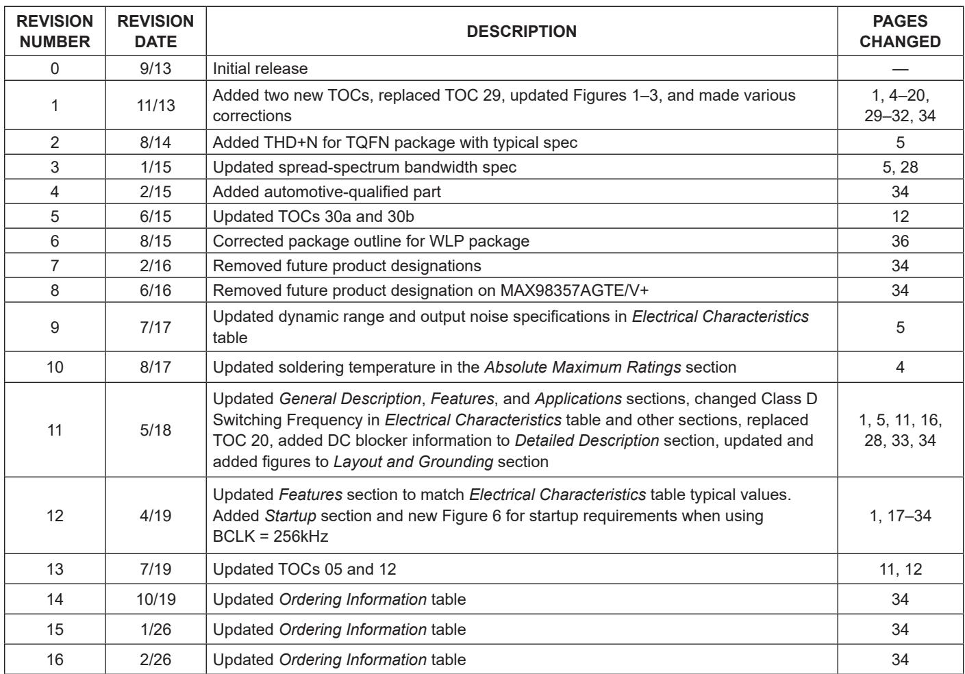
| REVISION NUMBER | REVISION DATE | DESCRIPTION | PAGES CHANGED |
| 0 | 9/13 | Initial release | — |
| 1 | 11/13 | Added two new TOCs, replaced TOC 29, updated Figures 1–3, and made various corrections | 1, 4–20, 29–32, 34 |
| 2 | 8/14 | Added THD+N for TQFN package with typical spec | 5 |
| 3 | 1/15 | Updated spread-spectrum bandwidth spec | 5, 28 |
| 4 | 2/15 | Added automotive-qualified part | 34 |
| 5 | 6/15 | Updated TOCs 30a and 30b | 12 |
| 6 | 8/15 | Corrected package outline for WLP package | 36 |
| 7 | 2/16 | Removed future product designations | 34 |
| 8 | 6/16 | Removed future product designation on MAX98357AGTE/V+ | 34 |
| 9 | 7/17 | Updated dynamic range and output noise specifications in Electrical Characteristics table | 5 |
| 10 | 8/17 | Updated soldering temperature in the Absolute Maximum Ratings section | 4 |
| 11 | 5/18 | Updated General Description, Features, and Applications sections, changed Class D Switching Frequency in Electrical Characteristics table and other sections, replaced TOC 20, added DC blocker information to Detailed Description section, updated and added figures to Layout and Grounding section | 1, 5, 11, 16, 28, 33, 34 |
| 12 | 4/19 | Updated Features section to match Electrical Characteristics table typical values. Added Startup section and new Figure 6 for startup requirements when using BCLK = 256kHz | 1, 17–34 |
| 13 | 7/19 | Updated TOCs 05 and 12 | 11, 12 |
| 14 | 10/19 | Updated Ordering Information table | 34 |
| 15 | 1/26 | Updated Ordering Information table | 34 |
| 16 | 2/26 | Updated Ordering Information table | 34 |
Figures and diagrams from the PDF
Preview the extracted datasheet assets and open any image in a separate tab for closer inspection.




Use this datasheet from any agent
Send the page, markdown, chunks, or search endpoint to ChatGPT, Claude, embedr-app, or your own tooling.