
INA233
36V, 16-Bit, Ultra-Precise I²C and PMBus Output Current, Voltage, Power, and Energy Monitor With Alert
INA233 36V, 16-Bit, Ultra-Precise I2C and PMBus Output Current, Voltage, Power, and Energy Monitor With Alert
1 Features
• Senses Bus Voltages From 0V to 36V
• High-Side or Low-Side Sensing
• Reports Current, Voltage, and Power
• Integrated Power Accumulator for Energy and Average Power Monitoring
• High Accuracy:
– 0.1% Gain Error (Max)
– 10µV Offset (Max)
• Configurable Averaging Options
• Independent Alert Limits for Current, Bus Voltage, and Power
• 1.8V Compliant I2C, SMBus, PMBus Interface
• 16 Programmable Addresses
• Operates From a 2.7V to 5.5V Power Supply
• 10-Pin, DGS (VSSOP) Package
2 Applications
• Servers
• Telecom Infrastructure
• High-Performance Computing
• Power Metering
• Battery Chargers
• Power Supply
• Test Equipment
3 Description
The INA233 device is a current, voltage, and power monitor with an I2C-, SMBus-, and PMBus-compatible interface that is compliant with digital bus voltages from 1.8V to 5.0V. The device monitors and reports values for current, voltage, and power. The integrated power accumulator can be used for energy or average power calculations. Programmable calibration value, conversion times, and averaging when combined with an internal multiplier enable direct readouts of current in amperes and power in watts.
The INA233 senses current on common-mode bus voltages that can vary from 0V to 36V, independent of the supply voltage. The device operates from a single 2.7V to 5.5V supply, drawing a typical supply current of 310µA in normal operation. The device can be placed in a low-power standby mode where the typical operating current is only 2µA. The device is specified over the operating temperature range between –40°C and +125°C and features up to 16 programmable addresses.
Package Information
| PART NUMBER | PACKAGE(1) | PACKAGE SIZE(2) |
| INA233 | DGS (VSSOP, 10) | 3.00mm × 4.90mm |
(1) For more information, see Section 10.
(2) The package size (length × width) is a nominal value and includes pins, where applicable.

High-Side or Low-Side Sensing Application
Table of Contents
1 Features....1
2 Applications....1
3 Description....1
4 Pin Configuration and Functions....3
5 Specifications....4
5.1 Absolute Maximum Ratings....4
5.2 ESD Ratings....4
5.3 Recommended Operating Conditions....4
5.4 Thermal Information....4
5.5 Electrical Characteristics....5
5.6 Typical Characteristics....7
6 Detailed Description....11
6.1 Overview....11
6.2 Functional Block Diagram....11
6.3 Feature Description....11
6.4 Device Functional Modes....13
6.5 Programming....15
6.6 Register Maps....23
7 Application and Implementation....41
7.1 Application Information....41
7.2 Typical Application....41
7.3 Power Supply Recommendations....43
7.4 Layout....44
8 Device and Documentation Support....45
8.1 Device Support....45
8.2 Documentation Support....45
8.3 Receiving Notification of Documentation Updates....45
8.4 Support Resources....45
8.5 Trademarks....45
8.6 Electrostatic Discharge Caution....45
8.7 Glossary....45
9 Revision History....45
10 Mechanical, Packaging, and Orderable Information....45
4 Pin Configuration and Functions

Figure 4-1. DGS Package 10-Pin VSSOP Top View
Table 4-1. Pin Functions
| PIN | Type | DESCRIPTION | |
| NAME | NO. | ||
| A0 | 2 | Digital input | Address pin. Connect to GND, SCL, SDA, or VS. Table 3 lists the pin settings and corresponding addresses. |
| A1 | 1 | Digital input | Address pin. Connect to GND, SCL, SDA, or VS. Table 3 lists the pin settings and corresponding addresses. |
| ALERT | 3 | Digital output | PMBus-compatible multifunctional alert, open-drain output. This pin alerts on independent settings for overcurrent, under- and overvoltage, and overpower conditions. |
| GND | 7 | Analog | Ground |
| IN- | 9 | Analog input | Connect to the load side of the shunt resistor |
| IN+ | 10 | Analog input | Connect to the supply side of the shunt resistor |
| SCL | 5 | Digital input | Serial bus clock line, open-drain input |
| SDA | 4 | Digital I/O | Serial bus data line, open-drain input/output |
| VBUS | 8 | Analog input | Bus voltage input |
| VS | 6 | Analog | Power supply, 2.7V to 5.5V |
5 Specifications
5.1 Absolute Maximum Ratings
over operating free-air temperature range (unless otherwise noted)(1)
| MIN | MAX | UNIT | ||
| $V_{VS}$ Supply voltage | 6 | V | ||
| Analog Inputs, IN+, IN- | $\text{Differential (V}_{\text{IN+}} - \text{V}_{\text{IN-}})^{(2)}$ | -40 40 | V | |
| Common-mode | -0.3 40 | |||
| $V_{VBUS}$ VBUS pin voltage | -0.3 | 40 | V | |
| $V_{SDA}$ | SDA, SCL pin voltages | GND - 0.3 | 6 | V |
| $V_A$ | A0, A1 pin voltages | GND - 0.3 | 6 | V |
| $I_{IN}$ | Input current into any pin | 5 | mA | |
| $I_{OUT}$ | Open-drain digital output current | 10 | mA | |
| $T_J$ | Junction temperature | 150 | °C | |
| $T_{stg}$ | Storage temperature | -65 | 150 | °C |
(1) Operation outside the Absolute Maximum Ratings may cause permanent device damage. Absolute Maximum Ratings do not imply functional operation of the device at these or any other conditions beyond those listed under Recommended Operating Conditions. If used outside the Recommended Operating Conditions but within the Absolute Maximum Ratings, the device may not be fully functional, and this may affect device reliability, functionality, performance, and shorten the device lifetime.
(2) IN+ and IN– can have a differential voltage between –40V and 40V. However, the voltage at these pins must not exceed the range of –0.3V to 40V.
5.2 ESD Ratings
| VALUE | UNIT | ||
| $V_{(ESD)}$ Electrostatic discharge | Human-body model (HBM), per ANSI/ESDA/JEDEC JS-001 $^{(1)}$ | ±2500 | V |
| Charged-device model (CDM), per JEDEC specification JESD22-C101 $^{(2)}$ | ±1000 | ||
(1) JEDEC document JEP155 states that 500V HBM allows safe manufacturing with a standard ESD control process.
(2) JEDEC document JEP157 states that 250V CDM allows safe manufacturing with a standard ESD control process.
5.3 Recommended Operating Conditions
over operating free-air temperature range (unless otherwise noted)
| MIN | NOM | MAX | UNIT | ||
| $V_{CM}$ | Common-mode input voltage | 0 | 36 | V | |
| $V_{VS}$ | Operating supply voltage | 2.7 | 5.5 | V | |
| $T_A$ | Operating free-air temperature | -40 | 125 | °C | |
5.4 Thermal Information
| THERMAL METRIC(1) | INA233 | UNIT | |
| DGS (VSSOP) | |||
| 10 PINS | |||
| $R_{\theta JA}$ | Junction-to-ambient thermal resistance | 171.4 | °C/W |
| $R_{\theta JC(top)}$ | Junction-to-case (top) thermal resistance | 42.9 | °C/W |
| $R_{\theta JB}$ | Junction-to-board thermal resistance | 91.8 | °C/W |
| $\psi_{JT}$ | Junction-to-top characterization parameter | 1.5 | °C/W |
| $\psi_{JB}$ | Junction-to-board characterization parameter | 90.2 | °C/W |
| $R_{\theta JC(bot)}$ | Junction-to-case (bottom) thermal resistance | n/a | °C/W |
(1) For more information about traditional and new thermal metrics, see the Semiconductor and IC Package Thermal Metrics application note.
5.5 Electrical Characteristics
t TA = 25°C, VVS = 3.3V, VIN+ = 12V, VSENSE = (VIN+ – VIN–) = 0mV, and VVBUS = 12V (unless otherwise noted)
| PARAMETER | TEST CONDITIONS | MIN | TYP | MAX | UNIT | |
| INPUT | ||||||
| Shunt voltage input range | -81.92 | 81.9175 | mV | |||
| Bus voltage input range(1) | 0 | 36 | V | |||
| CMRR | Common-mode rejection ratio | 0V ≤ VIN+ ≤ 36V | 126 | 140 | dB | |
| VOS | Offset voltage, RTI(2) | Shunt voltage | ±2.5 | ±10 | μV | |
| Bus voltage | ±1.25 | ±7.5 | mV | |||
| VOS (RTI(2)) vs temperature | Shunt voltage, -40°C ≤ TA ≤ +125°C | 0.02 | 0.1 | μV/°C | ||
| Bus voltage, -40°C ≤ TA ≤ +125°C | 10 | 40 | ||||
| PSRR | Power-supply rejection ratio (RTI(2)) | Shunt voltage, 2.7V ≤ VS ≤ 5.5V | 1 | μV/V | ||
| Bus voltage | 0.5 | mV/V | ||||
| IB | Input bias current (IN+, IN- pins) | 8 | μA | |||
| VBUS input impedance | 830 | kΩ | ||||
| Input leakage(3) | (IN+) + (IN-), power-down mode | 0.1 | 0.5 | μA | ||
| DC ACCURACY | ||||||
| ADC native resolution | 16 | Bits | ||||
| 1-LSB step size | Shunt voltage | 2.5 | μV | |||
| Bus voltage | 1.25 | mV | ||||
| Shunt voltage gain error | 0.02% | 0.1% | ||||
| Shunt voltage gain error vs temperature | -40°C ≤ TA ≤ +125°C | 5 | 25 | ppm/°C | ||
| Bus voltage gain error | 0.02% | 0.1% | ||||
| Bus voltage gain error vs temperature | -40°C ≤ TA ≤ +125°C | 10 | 50 | ppm/°C | ||
| Power gain error | VBUS = 12V, VIN+ - VIN- = -80mV to 80mV | 0.05% | 0.2% | |||
| Power gain error vs temperature | -40°C ≤ TA ≤ +125°C | 10 | 50 | ppm/°C | ||
| DNL | Differential nonlinearity | ±0.1 | LSB | |||
| tCT | ADC conversion time | CT bit = 000 | 140 | 154 | μs | |
| CT bit = 001 | 204 | 224 | ||||
| CT bit = 010 | 332 | 365 | ||||
| CT bit = 011 | 588 | 646 | ||||
| CT bit = 100 | 1.1 | 1.21 | ms | |||
| CT bit = 101 | 2.116 | 2.328 | ||||
| CT bit = 110 | 4.156 | 4.572 | ||||
| CT bit = 111 | 8.244 | 9.068 | ||||
| SMBus | ||||||
| SMBus timeout(4) | 28 | 35 | ms | |||
| DIGITAL INPUT/OUTPUT | ||||||
| Input capacitance | 3 | pF | ||||
| Leakage input current | $0V \leq V_{SCL} \leq V_{VS},$ $0V \leq V_{SDA} \leq V_{VS},$ $0V \leq V_{Alert} \leq V_{VS},$ $0V \leq V_{A0} \leq V_{VS},$ $0V \leq V_{A1} \leq V_{VS}$ | 0.5 | 2 | μA | ||
| $V_{IH}$ | High-level input voltage | SDA pin | 1.4 | 6 | V | |
| $V_{IL}$ | Low-level input voltage | SDA pin | -0.3 | 0.4 | V | |
| $V_{OL}$ | Low-level output voltage | $I_{OL} = 3mA, SDA and ALERT pins$ | 0 | 0.4 | V | |
| Hysteresis | 500 | mV | ||||
| POWER SUPPLY | ||||||
| Operating supply range | 2.7 | 5.5 | V | |||
| $I_Q$ | Quiescent current | 310 | 400 | μA | ||
| Quiescent current, power-down(shutdown) mode | 2 | 5 | μA | |||
| $V_{POR}$ | Power-on-reset (POR) threshold voltage | 2 | V | |||
(1) Although the input range is 36V, the full-scale range of the ADC scaling is 40.96V; see Section 6.3.1. Do not apply more than 36V. (2) RTI = Referred-to-input.
(3) Input leakage is positive (current flowing into the pin) for the conditions shown at the top of this table. Negative leakage currents can occur under different input conditions.
(4) SMBus timeout in the INA233 resets the interface whenever SCL is low for more than 28ms.
5.6 Typical Characteristics
at $\mathrm { T _ { A } } = 2 5 ^ { \circ } \mathrm { C } , \mathrm { V _ { V S } } = 3 . 3 \mathrm { V } , \mathrm { V _ { | N _ { + } } } = 1 2 \mathrm { V } , \mathrm { V _ { S E N S E } } = ( \mathrm { V _ { | N _ { + } } - V _ { | N _ { - } } } ) = 0 \mathrm { m V } , \mathrm { a n d V _ { V B U S } } = 1 2 \mathrm { V } , \mathrm { V _ { | N _ { + } } } = 0 . 3 \mathrm { V _ { | N _ { + } } } = 1 2 \mathrm { V _ { | N _ { + } } }$ (unless otherwise noted)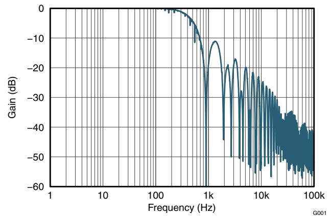

Figure 5-1. Frequency Response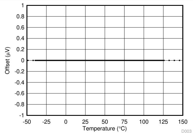
Figure 5-3. Shunt Input Offset Voltage vs Temperature
Figure 5-2. Shunt Input Offset Voltage Production Distribution
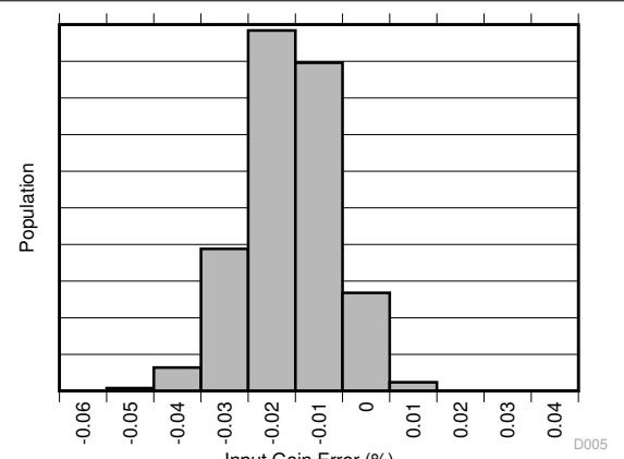
Figure 5-5. Shunt Input Gain Error Production Distribution
Figure 5-4. Shunt Input CMRR vs Temperature
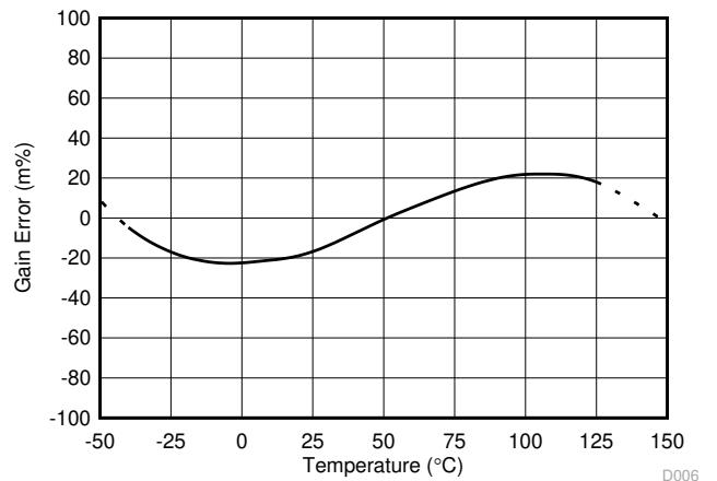
Figure 5-6. Shunt Input Gain Error vs Temperature
5.6 Typical Characteristics (continued)
$$
\text { at } T _ {\mathrm{A}} = 2 5 ^ {\circ} \mathrm{C}, V _ {\mathrm{VS}} = 3. 3 \mathrm{V}, V _ {\mathrm{IN+}} = 1 2 \mathrm{V}, V _ {\mathrm{SENSE}} = (V _ {\mathrm{IN+}} - V _ {\mathrm{IN-}}) = 0 \mathrm{mV}, \text { and } V _ {\mathrm{VBUS}} = 1 2 \mathrm{V} (\text { unless otherwise noted })
$$

Figure 5-7. Shunt Input Gain Error vs Common-Mode Voltage


Figure 5-9. Bus Input Offset Voltage vs Temperature
Figure 5-8. Bus Input Offset Voltage Production Distribution
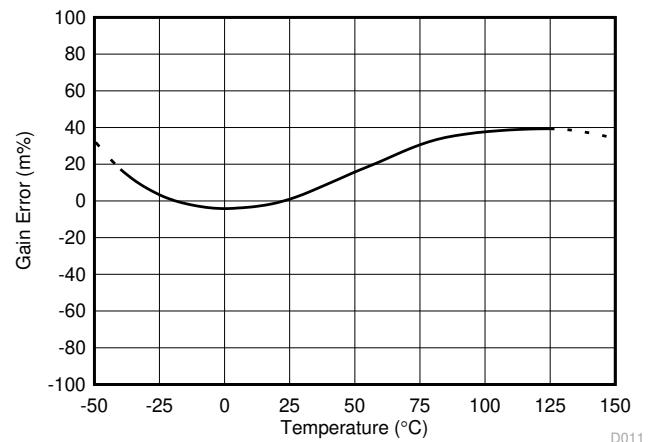
Figure 5-11. Bus Input Gain Error vs Temperature
Figure 5-10. Bus Input Gain Error Production Distribution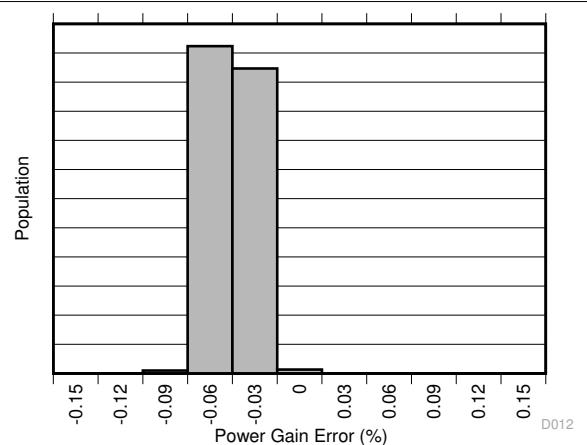
Figure 5-12. Power Gain Error Production Distribution
5.6 Typical Characteristics (continued)
$$
\text { at } T _ {\mathrm{A}} = 2 5 ^ {\circ} \mathrm{C}, V _ {\mathrm{VS}} = 3. 3 \mathrm{V}, V _ {\mathrm{IN+}} = 1 2 \mathrm{V}, V _ {\mathrm{SENSE}} = (V _ {\mathrm{IN+}} - V _ {\mathrm{IN-}}) = 0 \mathrm{mV}, \text { and } V _ {\mathrm{VBUS}} = 1 2 \mathrm{V} (\text { unless otherwise noted })
$$

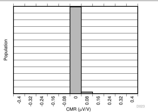
Figure 5-13. Power Gain Error vs Temperature
Figure 5-14. Input Common-Mode Rejection Distribution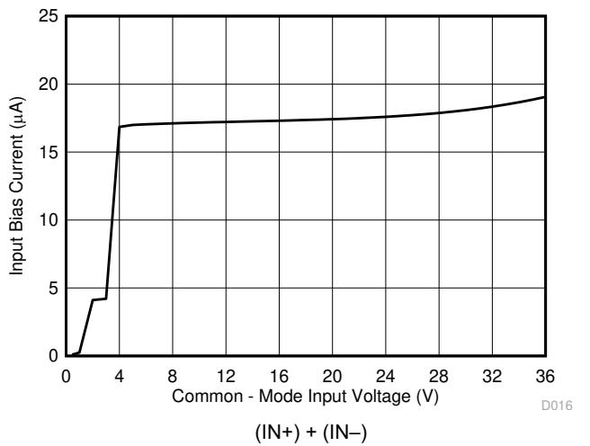
Figure 5-15. Power-Supply Rejection Distribution
Figure 5-17. Input Bias Current vs Temperature
Figure 5-16. Input Bias Current vs Common-Mode Voltage
Figure 5-18. Input Bias Shutdown Current vs Temperature
5.6 Typical Characteristics (continued)
at $\mathrm { T _ { A } } = 2 5 ^ { \circ } \mathrm { C } , \mathrm { V _ { V S } } = 3 . 3 \mathrm { V } , \mathrm { V _ { | N _ { + } } } = 1 2 \mathrm { V } , \mathrm { V _ { S E N S E } } = ( \mathrm { V _ { | N _ { + } } - V _ { | N _ { - } } } ) = 0 \mathrm { m V } , \mathrm { a n d V _ { V B U S } } = 1 2 \mathrm { V } , \mathrm { V _ { | N _ { + } } } = 0 . 3 \mathrm { V _ { | N _ { + } } } = 1 2 \mathrm { V _ { | N _ { + } } }$ (unless otherwise noted)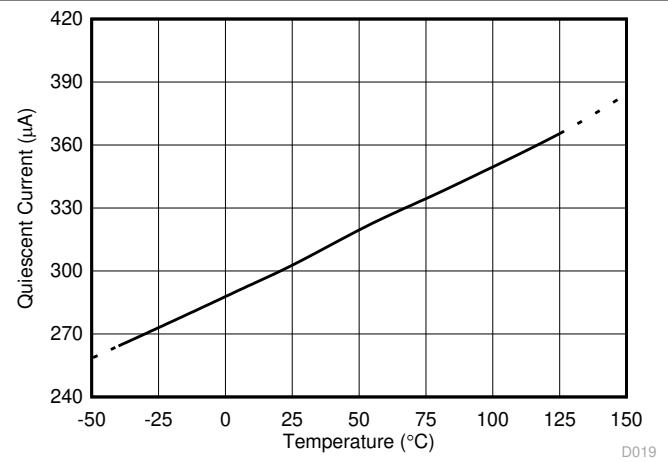
Figure 5-19. Active IQ vs Temperature


Figure 5-20. Shutdown IQ vs Temperature
Figure 5-22. Shutdown IQ vs SCL Frequency
Copyright © 2017, Texas Instruments Incorporated
6 Detailed Description
6.1 Overview
The INA233 is a digital current-sense amplifier with an $1 ^ { 2 } { \mathsf { C } } -$ , SMBus-, and PMBus-compatible interface. The device provides digital current, voltage, and power readings necessary for accurate decision-making in preciselycontrolled systems. The INA233 also has a built-in power accumulator that can be used for energy or average power measurements. Programmable out-of-range limits can be set to issue alerts when the voltage, current, or power is outside the normal range of operation. The integrated analog-to-digital converter (ADC) can be set to different averaging modes and configured for continuous-versus-triggered operation. The Register Maps section provides detailed register information for the INA233.
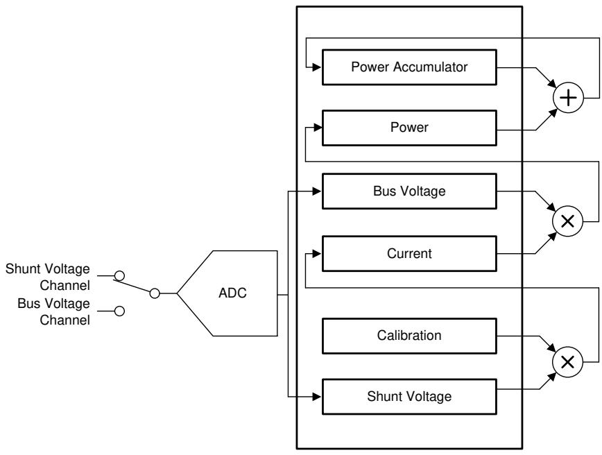
6.2 Functional Block Diagram
6.3 Feature Description
6.3.1 High-Accuracy Analog-to-Digital Convertor (ADC)
The INA233 integrates a highly accurate, 16-bit, delta-sigma (ΔΣ) ADC. This ADC is multiplexed to process both the shunt voltage and bus voltage measurements. The shunt voltage measurement is a differential measurement of the voltage developed when the load current flows through a shunt resistor as measured at the IN+ and IN– pins. The shunt voltage measurement has an maximum offset voltage of only 10 µV and a maximum gain error of only 0.1%. The low offset voltage of the shunt voltage measurement allows for increased accuracy at light load conditions for a given shunt resistor value. Another advantage of low offset is the ability to sense lower voltage drop across the sense resistor accurately, thus allowing for a lower-value shunt resistor. Lower-value shunt resistors reduce power loss in the current-sense circuit and help improve the power efficiency of the end application. The device can also measure the power-supply bus voltage by connecting this voltage to the VBUS pin. Internally, the voltage at VBUS is divided down to a voltage that can be measured by the ADC. The impedance of the VBUS pin to ground is approximately 830 kΩ. The differential shunt voltage is measured between the IN+ and IN– pins and the bus voltage is measured between the VBUS pin and GND.
The device takes two measurements: shunt voltage and bus voltage. The INA233 then converts these measurements to current, based on the calibration register value, and then calculates power; see the Calibration Register and Scaling section for additional information on programming the calibration register.
Although the device can be read at any time, and the data from the last conversion remain available, the conversion ready flag bit (MFR_ALERT_MASK, conversion ready bit) is provided to help coordinate one-shot or triggered conversions. The conversion ready bit is set after all conversions, averaging, and multiplication operations are complete.
The conversion ready bit clears under these conditions:
• Writing to the MFR_ADC_CONFIG register, except when configuring the MODE bits for power-down mode; or
• Reading the MFR_ALERT_MASK register
6.3.2 Interleaved Power Calculation
The current and shunt voltage measurements are interleaved to minimize time alignment errors in the power measurement. Figure 6-1 shows that power is calculated following the bus voltage measurement based on the previous current calculation and bus voltage measurement. The power calculation is performed in the background and does not add to the overall conversion times for bus voltage or current. These current and power values are considered intermediate results (unless the averaging is set to 1) and are stored in an internal accumulation register instead of the corresponding output registers. Following every measured sample, the newly-calculated values for current and power are appended to this accumulation register until all samples are measured and averaged based on the number of averages set in the MFR_ADC_CONFIG register.
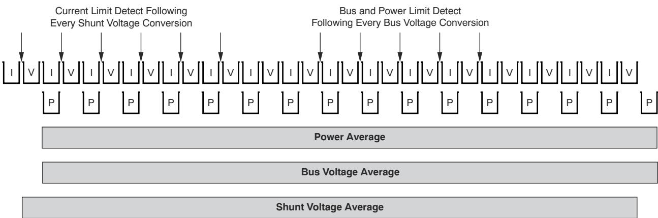
Figure 6-1. Power Calculation Scheme
In addition to the current and power accumulating after every sample, the shunt and bus voltage measurements are also collected. After all samples are measured and the corresponding current and power calculations are made, the accumulated average for each parameter is then loaded to the corresponding output registers and can then be read.
6.3.3 Power Accumulator and Energy Measurement
The INA233 has an integrated power accumulator that records the total accumulated power and the corresponding sample count and rollover counts. The accumulated power and sample count is accessible through the READ_EIN PMBus command and can be used for both energy metering and on-demand average power calculations. The READ_EIN section details how to use the power accumulator for both average power and energy calculations.
6.3.4 I2C-, SMBus-, and PMBus-Compatible Digital Interface
The INA233 features an I2C-compatible, 2-wire interface with an open-drain alert output. The data transfer format is SMBus version 3.0 compliant and the device supports multiple PMBus commands that allow the device to be easily used along side PMBus version 1.3 devices. Logic levels of 0.4 V (maximum $\mathsf { V } _ { \mathbb { L } } )$ and 1.4 V (minimum $\mathsf { V } _ { \sf I H } )$ allow the device to be used with digital bus voltages ranging from 1.8 V to 5.0 V (5.5-V maximum operating). The digital interface can support clock speeds as high as 400 kHz and offers packet error checking for increased communications robustness. The device supports group protocol as defined in the PMBus version 1.3.1 specification that allows the host processor to easily communicate with multiple devices on the bus.
6.3.5 Multiple Fault Event Reporting
The INA233 open-drain ALERT pin can report if any of the following errors simultaneously occur:
• Overcurrent warning
• Overpower warning
• Bus overvoltage warning
• Bus undervoltage warning
• Communication faults
• ADC overflow
• Conversion ready
The warning thresholds for the current, power, and bus voltages are set with the IOUT_OC_WARN_LIMIT, PIN_OP_WARN_LIMIT, VIN_UV_WARN_LIMIT, and VIN_OV_WARN_LIMIT standard PMBus commands. Various bus communications faults are supported as outlined in the STATUS_CML PMBus command.
The status for the conversion ready and ADC overflow bits can be monitored by the STATUS_MFR_SPECIFIC command. The conversion ready bit notifies when the device completes the previous conversion and is ready to begin a new conversion. Conversion ready can be monitored at the ALERT pin along with one of the alert functions. If an alert function and the conversion ready are both enabled to be monitored at the ALERT pin, then after the ALERT pin is asserted, the MFR_ALERT_MASK register or the PMBus status registers must be read following the alert to determine the source of the alert.
If the alert function is not used, the ALERT pin can be left floating without affecting device operation.
6.4 Device Functional Modes
6.4.1 Continuous Verses Triggered Operation
The internal ADC has two operating modes, continuous and triggered, that determine how the ADC operates following shunt voltage and bus voltage conversions. When the device is in normal operating mode, the INA233 continuously converts a shunt voltage reading followed by a bus voltage reading. After the shunt voltage reading, the current value is calculated. This current value is then used to calculate the power result. These values are subsequently stored in an accumulator, and the measurement and calculation sequence repeats until the number of averages set in the MFR_ADC_CONFIG register is reached. Following every sequence, the present set of values measured and calculated are appended to previously collected values. After all averaging completes, the final values for the shunt voltage, bus voltage, current, and power are updated in the corresponding registers that can then be read.
The MFR_ADC_CONFIG command allows for selecting modes that only convert the shunt voltage or the bus voltage to further allow the monitoring function to be configured to better fit the specific application requirements. This command also allows the device to be configured in continuous-versus-triggered operation. In triggered mode, writing any of the triggered convert modes into the MFR_ADC_CONFIG register triggers a single-shot conversion. This action produces a single set of measurements; thus, to trigger another single-shot conversion, the MFR_ADC_CONFIG register must be written to a second time, even if the mode does not change.
6.4.2 Device Shutdown
In addition to the two operating modes (continuous and triggered), the internal ADC also has a power-down mode that reduces the quiescent current and turns off current into the device inputs, reducing the effect of supply drain when the device is not being used. Full recovery from power-down mode requires 40 µs. The device registers can be written to and read from when the device is in power-down mode. The device remains in power-down mode until one of the active modes settings is selected using the MFR_ADC_CONFIG command.
6.4.3 Averaging and Conversion Time Considerations
The INA233 offers programmable conversion times (t ) for both the shunt voltage and bus voltage measurements. The conversion times for these measurements can be selected from as fast as 140µs to as long as 8.244ms. The conversion time settings, along with the programmable averaging mode, allow the device to be configured to optimize the available timing requirements in a given application. For example, if a system requires that data be read every 5ms, the device can be configured with the conversion times set to 588µs for both shunt and bus voltage measurements and the averaging mode set to 4. This configuration results in the data updating approximately every 4.7ms. The device can also be configured with a different conversion time setting for the shunt and bus voltage measurements. This type of approach is common in applications where the bus voltage tends to be relatively stable. This situation can allow for the time focused on the bus voltage measurement to be reduced relative to the shunt voltage measurement. The shunt voltage conversion time can be set to 4.156ms with the bus voltage conversion time set to 588µs and averaging mode set to 1. This configuration also results in data updating approximately every 4.7ms.
There are trade-offs associated with the settings for conversion time and the averaging mode used. The averaging feature can significantly improve the measurement accuracy by effectively filtering the signal. This approach allows the device to reduce any noise in the measurement that can be caused by noise coupling into the signal. A greater number of averages enables the device to be more effective in reducing the noise component of the measurement.
The conversion times selected can also have an effect on the measurement accuracy. Figure 6-2 shows multiple conversion times to illustrate the effect of noise on the measurement. to achieve the highest accuracy measurement possible, use a combination of the longest allowable conversion times and highest number of averages, based on the timing requirements of the system.
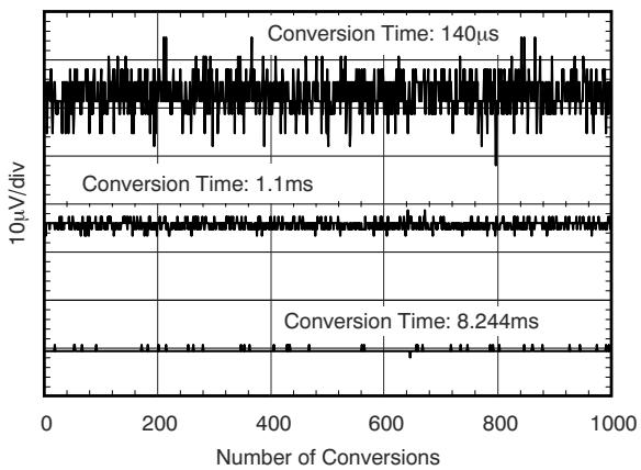
Figure 6-2. Noise vs Conversion Time
6.4.4 Filtering and Input Considerations
Measuring current is often noisy and such noise can be difficult to define. The INA233 offers several options for filtering by allowing the conversion times and number of averages to be selected independently in the MFR_ADC_CONFIG register. The conversion times can be set independently for the shunt voltage and bus voltage measurements to allow added flexibility when configuring the monitoring of the power-supply bus.
The internal ADC is based on a delta-sigma (ΔΣ) front-end with a 500kHz (±10% max) sampling rate. This architecture has good inherent noise rejection; however, transients that occur at or very close to the sampling rate harmonics can cause problems. These signals are at 1MHz and higher and can be managed by incorporating filtering at the device input. The high frequency enables the use of low-value series resistors on the filter with negligible effects on measurement accuracy. In general, filtering the device input is only necessary if there are transients at exact harmonics of the 500kHz (±10% max) sampling rate (greater than 1MHz). Filter using the lowest possible series resistance (typically 10Ω or less) and a ceramic capacitor. Recommended values for this capacitor are between 0.1µF and 1µF. Figure 6-3 illustrates the device with a filter added at the input.

Figure 6-3. Input Filtering
Overload conditions are another consideration for the device inputs. The device inputs are specified to tolerate 40V across the inputs. A large differential scenario can be a short to ground on the load side of the shunt. This type of event can result in full power-supply voltage across the shunt (as long the power supply or energy storage capacitors can support this voltage). Removing a short to ground can result in inductive kickbacks that can exceed the 40V differential and common-mode rating of the device. Inductive kickback voltages are best controlled by Zener-type, transient-absorbing devices (commonly called transzorbs) combined with sufficient energy storage capacitance. The Current Shunt Monitor with Transient Robustness Reference Design describes a high-side, current-shunt monitor used to measure the voltage developed across a current-sensing resistor and how to better protect the current-sense device from transient overvoltage conditions.
In applications that do not have large energy storage electrolytics on one or both sides of the shunt, an input overstress condition can result from an excessive dV/dt of the voltage applied to the input. A hard physical short is the most likely cause of this event, particularly in applications with no large electrolytics present. This problem occurs because an excessive dV/dt can activate the ESD protection in the device in systems where large currents are available. Testing demonstrates that the addition of 10Ω resistors in series with each input of the device sufficiently protects the inputs against this dV/dt failure up to the 40V rating of the device. Selecting these resistors in the range noted has minimal effect on accuracy.
6.5 Programming
The device can be used without any programming only when reading a shunt voltage drop and bus voltage with the default power-on reset configuration and with continuous conversion of the shunt and bus voltages.
Without setting the device register with the MFR_CALIBRATION command, the device is unable to provide either a valid current or power value because these outputs are both derived using the values loaded into the calibration register. The MFR_CALIBRATION command sets the current LSB size based on the desired full-scale range and value of the shunt resistor.
6.5.1 Default Settings
The default power-up states of the registers are shown in the Register Maps section. These registers are volatile and, if programmed to a value other than the default values listed in Table 6-4, must be reprogrammed at every device power-up. Detailed information on programming the calibration register specifically is given in the Programming section and calculated based on Equation 1.
6.5.2 Calibration Register and Scaling
An important aspect of the INA233 is that the device does not necessarily measure current or power. The device measures both the differential voltage applied between the IN+ and IN– input pins and the voltage applied to the VBUS pin. By correctly setting the calibration register scaling with the MFR_CALIBRATION command, returned values are calculated in voltage, amperes, and watts by scaling the returned value by the appropriate lest significant bit value (LSB) or by using the PMBus direct mode equation (Equation 3).
Equation 1 is used to obtain the value for the MFR_CALIGRATION register. This equation includes the term Current_LSB, which is the chosen value for the LSB for the READ_IIN command. As Equation 2 shows, the highest resolution for current measurements can be obtained by using the smallest allowable Current_LSB based on the maximum expected current. Although this value yields the highest resolution, the Current_LSB value is commonly selected as the nearest full number above this value to simplify the conversion of returned values for current and power to amperes and watts, respectively. The ${ \mathsf { R } } _ { \mathsf { S H U N T } }$ term is the value of the externa shunt used to develop the differential voltage across the input pins.
$$
\mathrm{CAL} = \frac {0 . 0 0 5 1 2}{\mathrm {Current_LSB} \times \mathrm {R_ {SHUNT}}}\tag{1}
$$
where
• 0.00512 is an internal fixed value used to verify that the scaling is maintained properly
$$
\text { Current_LSB } = \frac {\text { Maximum Expected Current }}{2 ^ {1 5}}\tag{2}
$$
After programming the calibration register, the values returned by the read current, power, and energy commands update accordingly based on the corresponding shunt voltage and bus voltage measurements.
Returned values for voltage, current, and power are calculated by multiplying the appropriate LSB value by the returned value, or can be calculated with PMBus coefficients as detailed in the Section 6.5.3 section. The size of the Power_LSB is internally set as 25 times the selected Current_LSB. The voltage LSB for bus voltage (READ_VIN and READ_VOUT commands) and shunt voltage (MFR_READ_VSHUNT) are fixed at 1.25mV/bit and 2.5µV/bit, respectively.
The MFR_CALIBRATION command allows the values returned by the READ_IIN and READ_PIN commands to be scaled to the most useful value for a given application. For example, set the MFR_CALIBRATION register so that the largest possible number is returned by the READ_IIN and READ_PIN commands at the expected full scale point. This approach yields the highest resolution using the previously calculated minimum Current_LSB in Equation 1. The calibration register can also be selected so that READ_IIN and READ_PIN return direct decima equivalents of the values being measured, or to yield a full LSB value for each corresponding register.
6.5.3 Reading and Writing Telemetry Data and Warning Thresholds
All telemetry data are measured using a 16-bit ADC. Telemetry data and user-programmed warning thresholds are communicated in 16-bit, two's compliment, signed data. Data are read or written in 2-byte increments conforming to the DIRECT format as described in section 8.3.3 of the PMBus Power System Management Protocol Specification 1.3 Part II. Device telemetry uses all 16 bits of the internal ADC; however, the warning registers only use the upper 12 bits for out-of-range comparisons. See each individual warning command (IOUT_OC_WARN_LIMIT, VIN_OV_WARN_LIMIT, VIN_UV_WARN_LIMIT, and PIN_OP_WARN_LIMIT) for the format of the warning threshold word.
6.5.4 Reading Telemetry Data and Warning Thresholds
Conversion from direct format to real-world dimensions of current, voltage, and power is accomplished by determining the appropriate coefficients as described in section 7.2.1 of the PMBus Power System Management Protocol Specification 1.3 Part II. According to this specification, the host system converts the received values using Equation 3 into a reading of volts, amperes, watts, or other such units.
$$
\mathrm{X} = \frac {1}{\mathrm{m}} \Big (\mathrm{Y} \times 1 0 ^ {- \mathrm{R}} - \mathrm{b} \Big)\tag{3}
$$
where
• X = the calculated real-world value (volts, amps, watts, and so forth)
• m = the slope coefficient
• Y = a 2-byte, two's complement integer received from the device
• b = the offset, which is a 2-byte, two's complement integer
• R = the exponent, which is a 1-byte, two's complement integer
• R is only necessary in systems where m is required to be an integer (for example, where m can be stored in a register of an integrated circuit) and R must only be large enough to yield the desired accuracy
The values for m and R (listed in Table 6-1) must be calculated for current and power measurements based off the selected value of the Current_LSB. For example, assume a Current_LSB of 0.75mA/bit is selected for a given application. The value for m is calculated by inverting the LSB value (for this case, m = 1 / 0.00075 = 1333.333). Moving the decimal point so the value of m is maximized and remains within the required range of –32768 to 32767 is preferable because this value of m is relatively small and contains decimal information. Moving the decimal point one place to the right results in a final m value of 13333 with an R value of –1 resulting from the shift in decimal location. Moving the decimal point to maximize the value of m is critical to minimize rounding errors. The m coefficient for power can be calculated by applying 1 / (25 × Current_LSB). For this example, the value for the m power coefficient is calculated to be 53.333. Again (to maximize accuracy), the decimal location is shifted by 2 to the right to give a final m value of 5333 with an R coefficient of –2. Care must be taken to adjust the exponent coefficient, R, such that the value of m remains within the range of –32768 to 32767. However, rounding errors resulting from the limitations on the value of m can be mitigated by carefully selecting a slightly higher current LSB size. For example, if a Current_LSB of 1mA/bit is selected instead of 0.75mA/bit, the calculated value for m is 1 / 0.001 or 1000; because this value is a whole number there is no rounding errors and the value for R is 0. Positive values for R signify the number of times the decimal point is shifted to the left, whereas negative values for R signify the number of decimal point shifts to the right.
Table 6-1. Telemetry and Warning Conversion Coefficients $( R _ { \mathbb { S } }$ in mΩ)
| COMMANDS | FORMAT | NUMBER OF DATA BYTES | m | b | R | UNIT |
| READ_VINVIN_OV_WARN_LIMITVIN_UV_WARN_LIMIT | DIRECT | 2 | 8 | 0 | 2 | V |
| READ_IIN, READ_IOUTMFR_IIN_OC_WARN_LIMIT | DIRECT | 2 | Calculated from Current_LSB | 0 | Calculated | A |
| READ_PIN, READ_EINMFR_PIN_OP_WARN_LIMIT | DIRECT | 2 | Calculated from Current_LSB | 0 | Calculated | W |
| MFR_READ_VSHUNT | DIRECT | 2 | 4 | 0 | 5 | V |
6.5.4.1 Writing Telemetry Data and Warning Thresholds
There are several PMBus commands that require writing telemetry data to be used. Use the same coefficients previously calculated for the application and apply these coefficients using Equation 4.
$$
Y = (m X + b) \times 1 0 ^ {R}\tag{4}
$$
where
• X = the real-world value (volts, amps, watts, temperature, and so forth)
• m = the slope coefficient, a 2-byte, two's complement integer
• Y = a 2-byte, two's complement integer written to the device
• b = the offset, which is a 2-byte, two's complement integer
• R = the exponent, which is a 1-byte, two's complement integer
6.5.5 System-Level Calibration With MFR_CALIRATION Command
The calibration register also offers possibilities for end-user, system-level calibration. After determining the exact current by using an external ammeter, the value of the MFR_CALIBRATION register can then be adjusted (see Equation 5) based on the measured current result of the INA233 to cancel the total system error.
$$
\text { Corrected_Full_Scale_Cal } = \text { trunc } \left(\frac {\text { Cal } \times \text { MeasShuntCurrent }}{\text { Device_Reported_Current }}\right)\tag{5}
$$
6.5.6 Bus Overview
The INA233 features an I2C-compatible, 2-wire interface with an open-drain Alert output. The data transfer format is SMBus version 3.0 compliant and the device supports multiple PMBus commands that allow the device to be easily used along with PMBus version 1.3 devices.
The device that initiates a data transfer is called a controller, and the devices controlled by the controller are targets. The bus must be controlled by a controller device that generates the serial clock (SCL), controls the bus access, and generates START and STOP conditions.
To address a specific device, the controller initiates a START condition by pulling the data signal line (SDA) from a high to a low logic level when SCL is high. All targets on the bus shift in the target address byte on the rising edge of SCL, with the last bit indicating whether a read or write operation is intended. During the ninth clock pulse, the target being addressed responds to the controller by generating an Acknowledge and pulling SDA low.
Data transfer is then initiated and eight bits of data are sent, followed by an Acknowledge bit. During data transfer, SDA must remain stable when SCL is high. Any change in SDA when SCL is high is interpreted as a START or STOP condition.
After all data are transferred, the controller generates a STOP condition, indicated by pulling SDA from low to high when SCL is high. The device includes a 28ms timeout on the interface to prevent bus lockup.
6.5.6.1 Serial Bus Address
To communicate with the INA233, the controller must first address target devices via a target address byte. The target address byte consists of seven address bits and a direction bit that indicates whether the action is to be a read or write operation.
The device has two address pins, A0 and A1. Table 6-2 lists the pin logic levels for each of the 16 possible addresses. The device samples the state of the A0 and A1 pins on every bus communication. Establish the pin states before any activity on the interface occurs.
Table 6-2. Address Pins and Target Addresses
| A1 | A0 | TARGETADDRESS |
| GND | GND | 1000000 |
| GND | VS | 1000001 |
| GND | SDA | 1000010 |
| GND | SCL | 1000011 |
| VS | GND | 1000100 |
| VS | VS | 1000101 |
| VS | SDA | 1000110 |
| VS | SCL | 1000111 |
| SDA | GND | 1001000 |
| SDA | VS | 1001001 |
| SDA | SDA | 1001010 |
| SDA | SCL | 1001011 |
| SCL | GND | 1001100 |
| SCL | VS | 1001101 |
| SCL | SDA | 1001110 |
| SCL | SCL | 1001111 |
6.5.6.2 Serial Interface
The INA233 operates only as a target device on both the I2C bus and the SMBus. Connections to the bus are made via the open-drain SDA and SCL lines. The SDA and SCL pins feature integrated spike-suppression filters and Schmitt triggers to minimize the effects of input spikes and bus noise. Although the device integrates spike suppression into the digital I/O lines, proper layout techniques help minimize the amount of coupling into the communication lines. This noise introduction can occur from capacitively coupling signal edges between the two communication lines themselves or from other switching noise sources present in the system. Routing traces in parallel with ground in between layers on a printed circuit board (PCB) typically reduces the effects of coupling between the communication lines. Shielded communication lines reduce the possibility of unintended noise coupling into the digital I/O lines that can be incorrectly interpreted as START or STOP commands.
All data bytes are transmitted least significant byte first.
6.5.6.3 Writing to and Reading From the INA233
Both writing and reading to the INA233 is accomplished through the use of various PMBus commands. Each PMBus command code is an address that allows read or write access to the internal registers; see the PMBus Command Support section for a complete list of supported PMBus commands and corresponding addresses. The value for the command address is the first byte transferred after the target address byte with the R/ W bit low. Every write operation to the device requires a value for the command address.
Writing to the device begins with the first byte transmitted by the controller. This byte is the target address with the R/ W bit low. The device then acknowledges receipt of a valid address. The next byte transmitted by the controller is the PMBus command address to the register that data are written to. This command address value updates the register pointer to the desired register. The next two bytes are written to the register addressed by the PMBus command. The device acknowledges receipt of each data byte. The controller can terminate data transfer by generating a START or STOP condition.
The timing structure for SEND BYTE commands is the same as WRITE WORD commands except no data packets are sent.
When reading from the device, first the device is written to with the desired PMBus command that is to return the desired value. This write is accomplished by issuing a target address byte with the R/ W bit low, followed by the PMBus command code. No additional data are required. The controller then generates a repeated START condition and sends the target address byte with the R/ W bit high to initiate the read command. The next byte is transmitted by the target and is the most significant byte of the register indicated by the register pointer. This byte is followed by an Acknowledge (ACK) from the controller; then the target transmits the least significant byte. The controller acknowledges receipt of the data byte. The controller can terminate data transfer by generating a Not-Acknowledge after receiving any data byte, or by generating a START or STOP condition. If repeated reads from the same register are desired, the register pointer bytes do not have to be continually sent; the device retains the register pointer value until the value is changed by the next write operation.
The READ BYTE format has the same timing structure as the READ WORD format except a byte of data is returned instead of a word.
Figure 6-4 shows the write operation timing diagram. Figure 6-5 shows the read operation timing diagram.

A. The value of the target address byte is determined by the settings of the A0 and A1 pins; see Table 6-2.
Figure 6-4. Timing Diagram for Write Word Format
A. The value of the target address byte is determined by the settings of the A0 and A1 pins; see Table 6-2.
B. Read data are from the previous PMBus command code.
C. An Acknowledge by the controller can also be sent.
Figure 6-5. Timing Diagram for Read Word Format
A block read is similar to the read word format in that first the device is written to with the desired PMBus command that is to return the desired value. This write is accomplished by issuing a target address byte with the R/ W bit low, followed by the PMBus command code. The controller then generates a repeated START condition and sends the target address byte with the R/ W bit high to initiate the read command. The next byte is transmitted by the target is the total number of bytes that are sent to the controller. This byte is followed by an Acknowledge (ACK) from the controller; then the target transmits the first data byte. At the end of each byte the controller sends an Acknowledge and the next byte is sent by the target. The controller can terminate data transfer by generating a Not-Acknowledge after receiving any data byte, or by generating a START or STOP condition.
Figure 6-6 shows the block read operation timing diagram. Figure 6-7 shows the timing diagram for the SMBus Alert response operation.

A. The value of the target address byte is determined by the settings of the A0 and A1 pins; see Table 6-2.
Figure 6-6. Timing Diagram for Block Read Format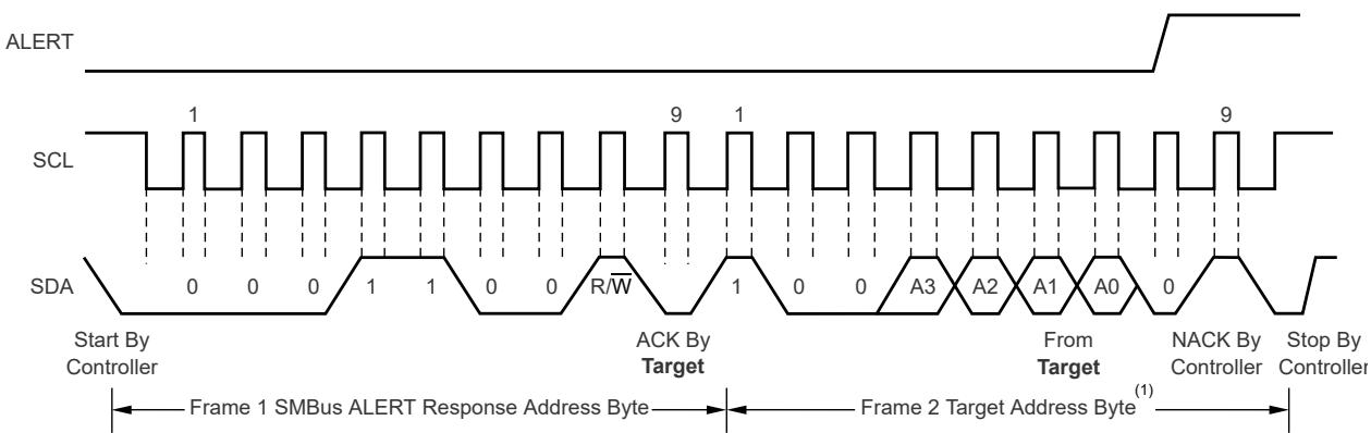
A. The value of the target address byte is determined by the settings of the A0 and A1 pins; see Table 6-2.
Figure 6-7. Timing Diagram for SMBus ALERT Response
6.5.6.3.1 Packet Error Checking
The INA233 supports packet error checking as described in the SMBus version 3.0 specification. Packet error checking is a method to improve the reliably and communication robustness of the digital interface. Packet error checking is implemented by appending a packet error code (PEC) at the end of each message transfer. To maximize compatibly, devices that support packet error checking must be able to communicate with the host and other devices that do not support the error checking protocol. Therefore, packet error checking can help improve the communication robustness when desired but is optional when not supported by the controller or other devices on the bus. See the SMBus version 3.0 specification for additional details on implementing packet error checking in an SMBus environment.
6.5.6.3.2 Bus Timing Requirements
When the bus is idle, both the SDA and SCL lines are pulled high by the pullup resistors. Figure 6-8 shows a timing diagram for the bus and Table 6-3 lists the bus timing definitions.
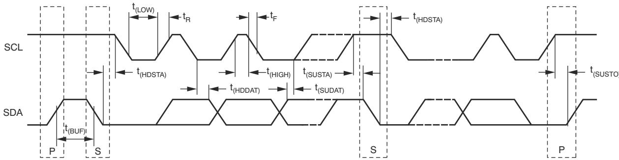
Figure 6-8. Bus Timing Diagram
Table 6-3. Bus Timing Definitions (1)
| MIN | MAX | UNIT | ||
| $f_{(SCL)}$ | SCL operating frequency | 10 | 400 | kHz |
| $t_{(BUF)}$ | Bus free time between STOP and START conditions | 0.6 | μs | |
| $t_{(HDSTA)}$ | Hold time after a repeated START condition. After this period, the first clock is generated. | 0.6 | μs | |
| $t_{(SUSTA)}$ | Repeated START condition setup time | 0.6 | μs | |
| $t_{(SUSTO)}$ | STOP condition setup time | 0.6 | μs | |
| $t_{(HDDAT)}$ | Data hold time | 0 | ns | |
| $t_{(SUDAT)}$ | Data setup time | 100 | ns | |
| $t_{(LOW)}$ | SCL clock low period | 1.3 | μs | |
| $t_{(HIGH)}$ | SCL clock high period | 0.6 | 50 | μs |
| $t_F$ | Data fall time | 300 | ns | |
| $t_F$ | Clock fall time | 300 | ns | |
| $t_R$ | Clock rise time | 300 | ns | |
(1) Values are based on a statistical analysis of a one-time sample of devices. Minimum and maximum values are not specified and are not production tested.
6.5.6.4 SMBus Alert Response
When SMBus alerts are latched, the INA233 is designed to respond to the SMBus alert response address. The SMBus alert response provides a quick fault identification for simple target devices. When an alert occurs, the controller can broadcast the alert response target address (0001 100) with the R/ W bit set high. Following this alert response, any target device that generates an alert is identified by acknowledging the alert response and sending the address on the bus.
The alert response can activate several different target devices simultaneously, similar to the $\mathsf { I 2 C }$ general call. If more than one target attempts to respond, bus arbitration rules apply and the device with the lowest address wins and is serviced first. The losing devices do not generate an Acknowledge and continue to hold the alert line low until the interrupt is cleared. The winning device responds with the address and releases the SMBus alert line. Even though the INA233 releases the SMBus line, the internal error flags are not cleared until the host clears the flags.
6.6 Register Maps
6.6.1 PMBus Command Support
The device features an SMBus interface that allows the use of PMBus commands to set warn levels, error masks, and obtain telemetry on bus voltage, current, power, and shunt voltage. Table 6-4 lists the supported PMBus commands.
Table 6-4. Supported PMBus Commands
| CODE | NAME | FUNCTION | R/W | NUMBER OF DATA BYTES | DEFAULT VALUE |
| 03h | CLEAR_FAULTS | Clears the status registers and rearms the black box registers for updating | Send byte | 0 | N/A |
| 12h | RESTORE_DEFAULT_ALL | Restores internal registers to the default values | Send byte | 0 | N/A |
| 19h | CAPABILITY | Retrieves the device capability | R | 1 | B0h |
| 4Ah | IOUT_OC_WARN_LIMIT | Retrieves or stores the output overcurrent warn limit threshold | R/W | 2 | 7FF8h |
| 57h | VIN_OV_WARN_LIMIT | Retrieves or stores the input overvoltage warn limit threshold | R/W | 2 | 7FF8h |
| 58h | VIN_UV_WARN_LIMIT | Retrieves or stores the input undervoltage warn limit threshold | R/W | 2 | 0000h |
| 6Bh | PIN_OP_WARN_LIMIT | Retrieves or stores the output overpower warn limit threshold | R/W | 2 | 7FF8h |
| 78h | STATUS BYTE | Retrieves information about the device operating status | R | 1 | 00h |
| 79h | STATUS_WORD | Retrieves information about the device operating status | R | 2 | 1000h |
| 7Bh | STATUS_IOUT | Retrieves information about the output current status | R/W, CLR | 1 | 00h |
| 7Ch | STATUS_INPUT | Retrieves information about the input status | R/W, CLR | 1 | 00h |
| 7Eh | STATUS_CML | Retrieves information about the communications status | R/W, CLR | 1 | 00h |
| 80h | STATUS_MFR_SPECIFIC | Retrieves information about the manufacturer specific device status | R/W, CLR | 1 | 20h |
| 86h | READ_EIN | Retrieves the energy reading measurement | Block read | 6 | 00h, 00h, 00h, 00h, 00h, 00h |
| 88h | READ_VIN | Retrieves the measurement for the VBUS voltage | R | 2 | 0000h |
| 89h | READ_IIN | Retrieves the input current measurement, supports both positive and negative currents | R | 2 | 0000h |
| 8Bh | READ_VOUT | Mirrors READ_VIN | R | 2 | 0000h |
| 8Ch | READ_IOUT | Mirror of READ_IIN for compatibility | R | 2 | 0000h |
| 96h | READ_POUT | Mirror of READ_PIN for compatibility with possible VBUS connections | R | 2 | 0000h |
| 97h | READ_PIN | Retrieves the input power measurement | R | 2 | 0000h |
| 99h | MFR_ID | Retrieves the manufacturer ID in ASCII characters (TI) | Block read | 2 | 54h, 49h |
| 9Ah | MFR_MODEL | Retrieves the device number in ASCII characters (INA233) | Block read | 6 | 49h, 4Eh, 41h, 32h, 33h, 33h |
| 9Bh | MFR_REVISION | Retrieves the device revision letter and number in ASCII (for instance, A0) | R | 2 | 41h, 30h |
| D0h | MFR_ADC_CONFIG | Configures the ADC averaging modes, conversion times, and operating modes | R/W | 2 | 4127h |
| D1h | MFR_READ_VSHUNT | Retrieves the shunt voltage measurement | R | 2 | 0000h |
| D2h | MFR_ALERT_MASK | Allows masking of device warnings | R/W | 1 | F0h |
| D4h | MFR_CALIBRATION | Allows the value of the current-sense resistor calibration value to be input. Must be programmed at power-up. Default value is set to 1. | R/W | 2 | 0001h |
| D5h | MFR_DEVICE_CONFIG | Allows the ALERT pin polarity to be changed | R/W | 1 | 02h |
| D6h | CLEAR_EIN | Clears the energy accumulator | Send byte | 0 | N/A |
| E0h | TI_MFR_ID | Returns a unique word for the manufacturer ID | R | 2 | ASCII TI, 5449h |
| E1h | TI_MFR_MODEL | Returns a unique word for the manufacturer model | R | 2 | ASCII 33 |
| E2h | TI_MFR_REVISION | Returns a unique word for the manufacturer revision | R | 2 | ASCII A0 |
6.6.2 Standard PMBus Commands
6.6.2.1 CLEAR_FAULTS (03h)
CLEAR_FAULTS is a standard PMBus command that resets all stored warning and fault flags and the alert signal. If a fault or warning condition still exists when the CLEAR_FAULTS command is issued, the ALERT signal clears but reasserts almost immediately. This command uses the PMBus send byte protocol.
6.6.2.2 RESTORE_DEFAULT_ALL (12h)
The RESTORE_DEFAULT_ALL command restores the internal device register settings to the default values.
Note
When issued, values in the calibration register are cleared and must be reconfigured by the controller.
6.6.2.3 CAPABILITY (19h)
The CAPABILITY command is a standard PMBus command that returns information about the PMBus functions supported by the INA233. This command is read with the PMBus read byte protocol.
Table 6-5. CAPABILITY Register
| VALUE | MEANING | DEFAULT |
| B0h | Supports packet error check, 400kbps, supports SMBus alert response address (ARA) | B0h |
6.6.2.4 IOUT_OC_WARN_LIMIT (4Ah) [default = 01111111 11111000]
This command is an overcurrent warn limit. This standard PMBus command is used to set or read the threshold of the first level warning of high output currents. Use the PMBus read or write word protocol to access this command. The contents of the IOUT_OC_WARN_LIMIT register are compared to the current-sense ADC telemetry value to detect high output current. This warning threshold applies to both positive and negative currents.
Enter the value in the register in amps with the same scaling and coefficients used for reading current.
When this input overcurrent warning limit is exceeded, the device:
• Sets the NONE OF THE ABOVE bit in the STATUS_BYTE register
• Sets the IOUT bit in the STATUS_WORD register
• Sets the IOUT_OC_WARNING bit in the STATUS_IOUT register
• Sets the INPUT bit in the STATUS_WORD register
• Sets the IIN_OC_WARNING bit in the STATUS_INPUT register
• Notifies (if unmasked) the host using the ALERT pin
This warning is masked with the MFR_ALERT_MASK command with the IIN_OC_WARN bit.
See the Reading and Writing Telemetry Data and Warning Thresholds and Writing Telemetry Data and Warning Thresholds sections for additional information on reading and setting warning thresholds.
Figure 6-9. IOUT_OC_WARN_LIMIT
| 15 | 14 | 13 | 12 | 11 | 10 | 9 | 8 |
| — | IO11 | IO10 | IO9 | IO8 | IO7 | IO6 | IO5 |
| R-0 | R/W-1 | R/W-1 | R/W-1 | R/W-1 | R/W-1 | R/W-1 | R/W-1 |
| 7 | 6 | 5 | 4 | 3 | 2 | 1 | 0 |
| IO4 | IO3 | IO2 | IO1 | IO0 | — | — | — |
| R/W-1 | R/W-1 | R/W-1 | R/W-1 | R/W-1 | R-0 | R-0 | R-0 |
Table 6-6. IOUT_OC_WARN_LIMIT Field Descriptions
| Bit | Field | Type | Default | Description |
| 15 | — | R | 0 | Reserved; always 0. |
| 14:3 | IO[11:0] | R/W | 1 | These bits control the IOUT_OC_WARN_LIMIT. The bit weightings in this register match the bit weightings in the READ_IOUT register (IO0 = II3). |
| 2:0 | — | R | 0 | Reserved; always 0. |
6.6.2.5 VIN_OV_WARN_LIMIT (57h) [default = 01111111 11111000]
VIN_OV_WARN_LIMIT is a standard PMBus command that allows configuring or reading the threshold for a VBUS overvoltage warning detection. Use the coefficients listed in Table 6-1 when reading and writing to this register. Use the PMBus read or write word protocol to access this command.
When this input overvoltage warning limit is exceeded, the device:
• Sets the NONE OF THE ABOVE bit in the STATUS_BYTE register
• Sets the INPUT bit in the STATUS_WORD register
• Sets the IOUT_OC_WARNING bit in the STATUS_INPUT register
• Notifies (if unmasked) the host using the ALERT pin
This fault is masked with the MFR_ALERT_MASK command using the VIN_OV_WARNING
See the Reading and Writing Telemetry Data and Warning Thresholds and Writing Telemetry Data and Warning Thresholds sections for additional information on reading and setting warning thresholds.
Full-scale range = 40.96 V (7FFFh) and LSB = 1.25 mV.
Figure 6-10. VIN_OV_WARN_LIMIT
| 15 | 14 | 13 | 12 | 11 | 10 | 9 | 8 |
| — | V11 | V10 | V9 | V8 | V7 | V6 | V5 |
| R-0 | R/W-1 | R/W-1 | R/W-1 | R/W-1 | R/W-1 | R/W-1 | R/W-1 |
| 7 | 6 | 5 | 4 | 3 | 2 | 1 | 0 |
| V4 | V3 | V2 | V1 | V0 | — | — | — |
| R/W-1 | R/W-1 | R/W-1 | R/W-1 | R/W-1 | R-0 | R-0 | R-0 |
Table 6-7. VIN_OV_WARN_LIMIT Field Descriptions
| Bit | Field | Type | Default | Description |
| 15 | — | R | 0 | Reserved; always 0. |
| 14:3 | V[11:0] | R/W | 1 | These bits control the VIN_OV_WARN_LIMIT. The bit weightings in this register match the bit weightings in the READ_VIN register (V0 = BV3). |
| 2:0 | — | R/W | 0 | Reserved; always 0. |
6.6.2.6 VIN_UV_WARN_LIMIT (58h) [default = 00000000 00000000]
VIN_UV_WARN_LIMIT is a standard PMBus command that allows configuring or reading the threshold for the VBUS undervoltage warning detection. Use the coefficients listed in Table 6-1 when reading and writing to this register. Use the PMBus read or write word protocol to access this command.
When this input undervoltage warning limit is exceeded, the device:
• Sets the NONE OF THE ABOVE bit in the STATUS_BYTE register
• Sets the INPUT bit in the STATUS_WORD register
• Sets the VIN_UV_WARNING bit in the STATUS_INPUT register
• Notifies (if unmasked) the host using the ALERT pin
This fault is masked with the MFR_ALERT_MASK command using the VIN_UV_WARNING bit.
See the Reading and Writing Telemetry Data and Warning Thresholds and Writing Telemetry Data and Warning Thresholds sections for additional information on reading and setting warning thresholds.
Full-scale range = 40.96 V (7FFFh) and LSB = 1.25 mV.
Figure 6-11. VIN_UV_WARN_LIMIT
| 15 | 14 | 13 | 12 | 11 | 10 | 9 | 8 |
| — | V11 | V10 | V9 | V8 | V7 | V6 | V5 |
| R-0 | R/W-0 | R/W-0 | R/W-0 | R/W-0 | R/W-0 | R/W-0 | R/W-0 |
| 7 | 6 | 5 | 4 | 3 | 2 | 1 | 0 |
| V4 | V3 | V2 | V1 | V0 | — | — | — |
| R/W-0 | R/W-0 | R/W-0 | R/W-0 | R/W-0 | R-0 | R-0 | R-0 |
Table 6-8. VIN_UV_WARN_LIMIT Field Descriptions
| Bit | Field | Type | Default | Description |
| 15 | — | R | 0 | Reserved; always 0. |
| 14:3 | V[11:0] | R/W | 0 | These bits control the VIN_UV_WARN_LIMIT. The bit weightings in this register match the bit weightings in the READ_VIN register (V0 = BV3). |
| 2:0 | — | R | 0 | Reserved; always 0. |
6.6.2.7 PIN_OP_WARN_LIMIT (6Bh) [default = 11111111 11110000]
PIN_OP_WARN_LIMIT is a standard PMBus command that allows setting or reading the threshold for the input overpower warning. Use the PMBus read or write word protocol to access the POUT_OP_WARN_LIMIT command. The contents of this register are compared to the calculated telemetry power value.
When the PIN_OP_WARN_LIMIT is exceeded, the device:
• Sets the INPUT bit in the upper byte of the STATUS_WORD register
• Sets the PIN_OP_WARNING bit in the STATUS_INPUT register
• Notifies the host by asserting the ALERT pin
This warning is masked with the MFR_ALERT_MASK command using the IIN_OP_WARNING bit.
Figure 6-12. PIN_OP_WARN_LIMIT
| 15 | 14 | 13 | 12 | 11 | 10 | 9 | 8 |
| D11 | D10 | D9 | D8 | D7 | D6 | D5 | D4 |
| R/W-1 | R/W-1 | R/W-1 | R/W-1 | R/W-1 | R/W-1 | R/W-1 | R/W-1 |
| 7 | 6 | 5 | 4 | 3 | 2 | 1 | 0 |
| D3 | D2 | D1 | D0 | — | — | — | — |
| R/W-1 | R/W-1 | R/W-1 | R/W-1 | R-0 | R-0 | R-0 | R-0 |
Table 6-9. PIN_OP_WARN_LIMIT Field Descriptions
| Bit | Field | Type | Default | Description |
| 15:4 | D[11:0] | R/W | 1 | These bits control the VIN_UV_WARN_LIMIT. The bit weightings in this register match the bit weightings in the READ_PIN register (D0 = P4). |
| 3:0 | — | R | 0 | Reserved; always 0. |
6.6.2.8 STATUS_BYTE (78h)
STATUS_BYTE is a standard PMBus command that returns the value of a number of flags indicating the state of the INA233. Use the PMBus read byte protocol to access this command. To clear bits in this register, clear the underlying fault and issue a CLEAR_FAULTS command. Table 6-10 lists the definitions for this command.
Table 6-10. STATUS_BYTE Definitions
| BIT | NAME | MEANING | DEFAULT |
| 7 | BUSY | Not supported | 0 |
| 6 | OFF | Not supported | 0 |
| 5 | VOUT_OV | Not supported | 0 |
| 4 | IOUT_OC | Not supported | 0 |
| 3 | VIN_UV | Not supported | 0 |
| 2 | TEMPERATURE | Not supported | 0 |
| 1 | CML | A communication fault has occurred | 0 |
| 0 | NONE OF THE ABOVE | A fault or warning not listed in bits[7:1] has occurred | 0 |
NONE OF THE ABOVE (bit 0) is set by the logical OR of the following status bits from other registers:
• IOUT_OC_WARNING
• VIN_OV_WARNING
• VIN_UV_WARNING
• IIN_OC_WARNING
This bit can only be cleared by clearing all the contributing status bits.
6.6.2.9 STATUS_WORD (79h)
STATUS_WORD is a standard PMBus command that returns the value of a number of flags indicating the state of the INA233. Use the PMBus read word protocol to access this command. To clear bits in this register, clear the underlying fault and issue a CLEAR_FAULTS command. The INPUT and VIN UV flags default to 1 on startup. Table 6-11 lists the definitions for this command.
Table 6-11. STATUS_WORD Definitions
| BIT | NAME | MEANING | DEFAULT |
| 15 | VOUT | Not supported | 0 |
| 14 | IOUT/POUT | An output current or power warning has occurred | 0 |
| 13 | INPUT | An input voltage, current, or power warning has occurred | 0 |
| 12 | MFR | A manufacturer-specific fault or warning has occurred | 1 |
| 11 | POWER_GOOD# | Not supported | 0 |
| 10 | FANS | Not supported | 0 |
| 9 | OTHER | Not supported | 0 |
| 8 | UNKNOWN | Not supported | 0 |
| 7 | BUSY | Not supported | 0 |
| 6 | OFF | Not supported | 0 |
| 5 | VOUT_OV | Not supported | 0 |
| 4 | IOUT_OC | Not supported | 0 |
| 3 | VIN_UV | Not supported | 0 |
| 2 | TEMPERATURE | Not supported | 0 |
| 1 | CML | A communication fault has occurred | 0 |
| 0 | NONE OF THE ABOVE | A fault or warning not listed in bits[7:1] has occurred | 0 |
6.6.2.10 STATUS_IOUT (7Bh)
STATUS_IOUT is a standard PMBus command that returns the value of the of a number of flags related to output, current, and power. Use the PMBus read byte protocol to access this command. To clear bits in this register, clear the underlying fault and issue a CLEAR_FAULTS command or write a 1 to the bit to be cleared. Table 6-12 lists the definitions for this command.
Table 6-12. STATUS_IOUT Definitions
| BIT | NAME | MEANING | DEFAULT |
| 7 | IOUT_OC fault | Not supported | 0 |
| 6 | IOUT_OC fault with LV shutdown | Not supported | 0 |
| 5 | IOUT_OC_WARN | An input undercurrent warning has occurred | 0 |
| 4 | IOUT_UC fault | Not supported | 0 |
| 3 | Current share fault | Not supported | 0 |
| 2 | In power-limiting mode | Not supported | 0 |
| 1 | POUT_OP fault | Not supported | 0 |
| 0 | POUT_OP_WARN | Not supported | 0 |
6.6.2.11 STATUS_INPUT (7Ch)
STATUS_INPUT is a standard PMBus command that returns the value of the of a number of flags related to input voltage, current, and power. Use the PMBus read byte protocol to access this command. To clear bits in this register, clear the underlying fault and issue a CLEAR_FAULTS command or write a 1 to the bit to be cleared. Table 6-13 lists the definitions for this command.
Table 6-13. STATUS_INPUT Definitions
| BIT | NAME | MEANING | DEFAULT |
| 7 | VIN_OV fault | Not supported | 0 |
| 6 | VIN_OV_WARN | An input overvoltage warning has occurred | 0 |
| 5 | VIN_UV_WARN | An input undervoltage warning has occurred | 0 |
| 4 | VIN_UV fault | Not supported | 0 |
| 3 | Insufficient voltage | Not supported | 0 |
| 2 | IIN_OC fault | Not supported | 0 |
| 1 | IIN_OC_WARN | An input overcurrent warning has occurred | 0 |
| 0 | PIN_OP_WARN | An input overpower warning has occurred | 0 |
6.6.2.12 STATUS_CML (7Eh)
STATUS_CML is a standard PMBus command that returns the value of a number of flags related to communication faults. Use the PMBus read byte protocol to access this command. To clear bits in this register, issue a CLEAR FAULTS command or write a 1 to the bit to be cleared. Table 6-14 lists the definitions for this command.
Table 6-14. STATUS_CML Definitions
| BIT | MEANING | DEFAULT |
| 7 | Invalid or unsupported command received | 0 |
| 6 | Not supported | 0 |
| 5 | Packet error check failed | 0 |
| 4 | Memory fault detected (trim fuse CRC failed, ECC active) | 0 |
| 3 | Not supported | 0 |
| 2 | Reserved | 0 |
| 1 | Not supported | 0 |
| 0 | Not supported | 0 |
6.6.2.13 STATUS_MFR_SPECIFIC (80h)
STATUS_MFR_SPECIFIC is a standard PMBus command that contains manufacturer-specific status information. Use the PMBus read byte protocol to access this command. To clear bits in this register, clear the underlying fault and issue a CLEAR_FAULTS command or write a 1 to the bit to be cleared. Table 6-15 lists the definitions for this command.
Table 6-15. STATUS_MFR_SPECIFIC Definitions
| BIT | MEANING | DEFAULT |
| 7 | Conversion ready | 0 |
| 6 | Arithmetic overflow flag. If the bit is set to 1 then an arithmetic operation results from an overflow error. This bit indicates that either the current or power data is invalid. | 0 |
| 5 | Power-on-reset event detected. To detect power-on or power glitch events, this bit must be cleared after initial power up. If power is interrupted this bit is reset to the default value of 1. | 1 |
| 4 | Communications or memory fault (or of STATUS_CML) | 0 |
| 3 | Input overpower warning | 0 |
| 2 | Input overcurrent warning | 0 |
| 1 | Input overvoltage warning | 0 |
| 0 | Input undervoltage warning | 0 |
6.6.2.14 READ_EIN (86h)
READ_EIN is a command that returns information that the host can use to calculate energy or to average input power consumption. Use the PMBus block read protocol to access this command. Six bytes of data are returned by this command. The first two bytes are the 16-bit, unsigned output of an accumulator that continuously sums samples of the instantaneous input power. These two data bytes are formatted such that returned values can be converted to watts using the power m, b, and R coefficients. The third data byte is a count of the rollover events for the accumulator. This byte is an unsigned integer indicating the number of times that the accumulator has rolled over from the maximum positive value (FFFFh) to zero. The last three data bytes are a 24-bit unsigned integer that counts the number of samples of the instantaneous input power that are applied to the accumulator.
The combination of the accumulator and the rollover count can overflow within a few seconds depending on the ADC conversion time. The host software must detect and appropriately handle this overflow. Similarly, the sample count value overflows, but this event only occurs one time every few hours using 1ms ADC conversion times.
To convert the data obtained with the READ_EIN command to average power, first convert the accumulator and rollover count to an unsigned integer.
$$
\text { Total Accumulated Unscaled Power(Accumulator_24) = (rollover_count\times 2 ^ {16}) + Accumulator}
$$
Overflow detection and handling are done on the 24 bits of accumulator data and the sample count now. As shown in Equation $^ { 6 , }$ data from the previous calculation must be saved and used in this calculation to obtain the unscaled average power. Table 6-16 lists the definitions for this command.
$$
\frac {\text {Accumulator_24} [ n ] - \text {Accumulator_24} [ n - 1 ]}{\text {Sample_count} [ n ] - \text {Sample_count} [ n - 1 ]}\tag{6}
$$
where
• accumulator_24 [n] = Overflow corrected, 24-bit accumulator data from this read
• Sample_count [n] = Sample count data from this read
• accumulator_24[n-1] = Overflow corrected 24-bit accumulator data from the previous read Sample_count [n-1] = Sample count data from the previous read
• Unscaled average power is now in the same units as the data from the READ_PIN command
• PMBus coefficients are used to convert the unscaled average power to watts
Table 6-16. READ_EIN Definitions
| BYTE | MEANING | DEFAULT |
| 6 | Sample count high byte | 0 |
| 5 | Sample count mid byte | 0 |
| 4 | Sample count low byte | 0 |
| 3 | Power accumulator rollover count | 0 |
| 2 | Power accumulator high byte | 0 |
| 1 | Power accumulator low byte | 0 |
| 0 | Number of bytes | 6 |
When the average power is calculated over a known number of samples, energy can be calculated by taking the product of the average power and the time interval for that average. The time interval can be externally measured or calculated by multiplying the number of samples reported by the ADC conversion time inclusive of any device averaging modes. However, calculating the energy consumption using the ADC conversion time results in a 10% error in the energy reading because of variations in the internal sampling oscillator. For increased precision in the energy measurement, using a higher accuracy external time measurement method is recommended.
The energy accumulator can be configured by the MFR_DEVICE_CONFIG command to automatically clear with each READ_EIN command. The ability to clear the accumulator on a read permits the device to be easily synchronised to an external timer and allows the accumulator to always start at 0, thus eliminating the need to subtract the initial accumulated values and sample counts.
The READ_EIN power accumulator can also be cleared by issuing a CLEAR_EIN command or RESTORE_DEFAULTS_ALL command. Clearing the power accumulator with the RESTORE_DEFAULTS_ALL command is not recommended because this command also clears the calibration register used to scale the accumulated power.
6.6.2.15 READ_VIN (88h)
READ_VIN is a standard PMBus command that returns the 16-bit measured value of the input voltage as read from the VBUS pin. Use the coefficients listed in Table 6-1 to read this register. Use the PMBus read word protocol to access this command. This value is also used internally for the VIN_OV_WARN and VIN_UV_WARN detection.
Table 6-17. READ_VIN Register
| VALUE | MEANING | DEFAULT |
| 0h–7FFFh | Measured value for VBUS | 0000h |
Full-scale range = 40.96V (7FFFh) and LSB = 1.25mV.
6.6.2.16 READ_IIN (89h)
READ_IIN is a standard PMBus command that returns the 16-bit signed value of the sensed current. Use the PMBus read word protocol to access this command. This value is also used internally for the IOUT_OC_WARN detection.
Table 6-18. READ_IIN Register
| VALUE | MEANING | DEFAULT |
| 0000h-FFFFh | Measured value for $I_{IN}$ | 0000h |
If averaging is enabled, this register displays the averaged value. The value returned by the READ_IIN command is calculated by multiplying the decimal value in the READ_VHSUNT_OUT register with the decimal value of the MFR_CALIBRATION register.
6.6.2.17 READ_VOUT (8Bh)
This command is a mirror of the READ_VIN command supported for cases where VBUS is connected to the output.
6.6.2.18 READ_IOUT (8Ch, R)
This command is a mirror of the READ_IOUT command for software compatibility.
6.6.2.19 READ_POUT (96h, R)
READ_POUT is mirror of the READ_PIN command to support applications that connect the VBUS pin to the output.
6.6.2.20 READ_PIN (97h, R)
READ_PIN is a standard PMBus command that returns the 16-bit measured unsigned absolute value of the input power when VBUS is connected to the input.
Use the PMBus read word protocol to access this command. This value is also used internally for the POUT_OP_WARN detection.
Table 6-19. READ_PIN Register
| VALUE | MEANING | DEFAULT |
| 0h-FFFFh | Measured value for PIN | 0000h |
6.6.2.21 MFR_ID (99h)
MFR_ID is a standard PMBus command that returns the identification of the manufacturer. Use the PMBus block read protocol to read the manufacturer ID.
Table 6-20. MFR_ID Register
| BYTE | NAME | VALUE |
| 0 | Number of bytes | 02h |
| 1 | MFR ID-1 | 54h, ASCII (T) |
| 2 | MFR ID-2 | 49h, ASCII (I) |
6.6.2.22 MFR_MODEL (9Ah)
MFR_MODEL is a standard PMBus command that returns the part number of the device. Use the PMBus block read protocol to read the manufacturer model.
Table 6-21. MFR_MODEL Register
| BYTE | NAME | VALUE |
| 0 | Number of bytes | 06h |
| 1 | MFR MODEL-1 | 49h, ASCII (I) |
| 2 | MFR MODEL-2 | 4Eh, ASCII (N) |
| 3 | MFR MODEL-3 | 41h, ASCII (A) |
| 4 | MFR MODEL-4 | 32h, ASCII (2) |
| 5 | MFR MODEL-5 | 33h, ASCII (3) |
| 6 | MFR MODEL-6 | 33h, ASCII (3) |
6.6.2.23 MFR_REVISION (9Bh)
MFR_REVISION is a standard PMBus command that returns the revision level of the device. Use the PMBus block read protocol to read the manufacturer revision.
Table 6-22. MFR_REVISION Register
| BYTE | NAME | VALUE |
| 0 | Number of bytes | 02h |
| 1 | MFR REV-1 | 41h, ASCII (A) |
| 2 | MFR REV-2 | 41h, ASCII (0) |
6.6.3 Manufacturer-Specific PMBus Commands
6.6.3.1 MFR_ADC_CONFIG (D0h) [default = 01000001 00100111]
The MFR_ADC_CONFIG command settings control the operating modes for the device ADC. This command controls the conversion time settings for both the shunt and bus voltage measurements as well as the averaging mode used. The operating mode that controls what signals are selected to be measured is also set with this command. Reading with the MFR_ADC_CONFIG command can be done at any time without affecting the device settings or a conversion in progress. Writing with the MFR_ADC_CONFIG command halts any conversion in progress until the write sequence is completed, resulting in a new conversion starting based on the updated contents. This halt prevents any uncertainty in the conditions used for the next completed conversion.
Figure 6-13. MFR_ADC_CONFIG
| 15 | 14 | 13 | 12 | 11 | 10 | 9 | 8 |
| — | — | — | — | AVG2 | AVG1 | AVG0 | VBUSCT2 |
| R-0 | R-1 | R-0 | R-0 | R/W-0 | R/W-0 | R/W-0 | R/W-1 |
| 7 | 6 | 5 | 4 | 3 | 2 | 1 | 0 |
| VBUSCT1 | VBUSCT0 | VSHCT2 | VSHCT1 | VSHCT0 | MODE3 | MODE2 | MODE1 |
| R/W-0 | R/W-0 | R/W-1 | R/W-0 | R/W-0 | R/W-1 | R/W-1 | R/W-1 |
Table 6-23. MFR_ADC_CONFIG Field Descriptions
| Bit | Field | Type | Default | Description |
| 15 | — | R | 0 | Reserved. |
| 14 | 1 | |||
| 13:12 | 0 | |||
| 11 | AVG2 | R/W | 0 | Averaging mode. These bits determine the number of samples that are collected and averaged. Table 6-24 lists AVG bit settings and related number of averages for each bit setting. |
| 10 | AVG1 | R/W | 0 | |
| 9 | AVG0 | R/W | 0 | |
| 8 | VBUSCT2 | R/W | 1 | Bus voltage conversion time. These bits set the conversion time for the bus voltage measurement. Table 6-25 lists the VBUSCT bit options and related conversion times for each bit setting. |
| 7 | VBUSCT1 | R/W | 0 | |
| 6 | VBUSCT0 | R/W | 0 | |
| 5 | VSHCT2 | R/W | 1 | Shunt voltage conversion time. These bits set the conversion time for the shunt voltage measurement. Table 6-26 lists the VSHCT bit options and related conversion times for each bit setting. |
| 4 | VSHCT1 | R/W | 0 | |
| 3 | VSHCT0 | R/W | 0 | |
| 2:0 | MODE[3:1] | R/W | 1 | Operating mode. These bits select the continuous, triggered, or power-down mode of operation. These bits default to continuous shunt and bus measurement mode. Table 6-27 lists the mode settings. |
Table 6-24. AGV[2:0] Bit Setting Combinations
| AVG2 | AVG1 | AVG0 | NUMBER OF AVERAGES |
| 0 (default) | 0 (default) | 0 (default) | 1 (default) |
| 0 | 0 | 1 | 4 |
| 0 | 1 | 0 | 16 |
| 0 | 1 | 1 | 64 |
| 1 | 0 | 0 | 128 |
| 1 | 0 | 1 | 256 |
| 1 | 1 | 0 | 512 |
| 1 | 1 | 1 | 1024 |
Table 6-25. VBUSCT[2:0] Bit Setting Combinations
| VBUSCT2 | VBUSCT1 | VBUSCT0 | CONVERSION TIME |
| 0 | 0 | 0 | 140 μs |
| 0 | 0 | 1 | 204 μs |
| 0 | 1 | 0 | 332 μs |
| 0 | 1 | 1 | 588 μs |
| 1 (default) | 0 (default) | 0 (default) | 1.1 ms (default) |
| 1 | 0 | 1 | 2.116 ms |
| 1 | 1 | 0 | 4.156 ms |
| 1 | 1 | 1 | 8.244 ms |
Table 6-26. VSHCT[2:0] Bit Setting Combinations
| VSHCT2 | VSHCT1 | VSHCT0 | CONVERSION TIME |
| 0 | 0 | 0 | 140 μs |
| 0 | 0 | 1 | 204 μs |
| 0 | 1 | 0 | 332 μs |
| 0 | 1 | 1 | 588 μs |
| 1 (default) | 0 (default) | 0 (default) | 1.1 ms (default) |
| 1 | 0 | 1 | 2.116 ms |
| 1 | 1 | 0 | 4.156 ms |
| 1 | 1 | 1 | 8.244 ms |
Table 6-27. Mode[3:1] Bit Settings Combinations
| MODE3 | MODE2 | MODE1 | MODE |
| 0 | 0 | 0 | Power-down (or shutdown) |
| 0 | 0 | 1 | Shunt voltage, triggered |
| 0 | 1 | 0 | Bus voltage, triggered |
| 0 | 1 | 1 | Shunt and bus, triggered |
| 1 | 0 | 0 | Power-down (or shutdown) |
| 1 | 0 | 1 | Shunt voltage, continuous |
| 1 | 1 | 0 | Bus voltage, continuous |
| 1 (default) | 1 (default) | 1 (default) | Shunt and bus, continuous (default) |
6.6.3.2 MFR_READ_VSHUNT (D1h) [default = 00000000 00000000]
This register stores the current shunt voltage reading, VSHUNT. Negative numbers are represented in two'scomplement format. Generate the two's complement of a negative number by complementing the absolute value binary number and adding 1. An MSB = 1 denotes a negative number.
If averaging is enabled, this register displays the averaged value. Full-scale range = 81.92 mV (7FFFh) and LSB: 2.5 µV.
This command only supports the PMBus direct data format.
Figure 6-14. MFR_READ_VSHUNT
| 15 | 14 | 13 | 12 | 11 | 10 | 9 | 8 |
| Sign | SD14 | SD13 | SD12 | SD11 | SD10 | SD9 | SD8 |
| R-0 | R-0 | R-0 | R-0 | R-0 | R-0 | R-0 | R-0 |
| 7 | 6 | 5 | 4 | 3 | 2 | 1 | 0 |
| SD7 | SD6 | SD5 | SD4 | SD3 | SD2 | SD1 | SD0 |
| R-0 | R-0 | R-0 | R-0 | R-0 | R-0 | R-0 | R-0 |
Table 6-28. MFR_READ_VSHUNT Field Descriptions
| Bit | Field | Type | Default | Description |
| 15 | Sign | R | 0 | This bit determines the sign for the returned value.0 = Positive1 = Negative |
| 14:0 | SD[14:0] | R | 0 | These bits set the shunt voltage data. |
6.6.3.3 MFR_ALERT_MASK (D2h) [default = XXXXXXXX 11110000]
The bits in this register correspond to the bits in the STATUS_MFR_SPECIFIC register. Setting a bit in this register blocks the corresponding bit in the STATUS_MFR_SPECIFIC register from having an effect on the ALERT pin.
Figure 6-15. MFR_ALERT_MASK
| 7 | 6 | 5 | 4 | 3 | 2 | 1 | 0 |
| Conversion ready | ADC overflow detected | POR event detected | Communications | IN_OP_WARNING | IN_OC_WARNING | IN_OV_WARNING | IN_UV_WARNING |
| R/W-1 | R-1 | R-1 | R/W-1 | R/W-0 | R/W-0 | R/W-0 | R/W-0 |
Table 6-29. MFR_ALERT_MASK Field Descriptions
| Bit | Field | Type | Default | Description |
| 7 | Conversion ready | R/W | 1 | Masks the conversion ready signal to the ALERT pin (masked by default). |
| 6 | ADC overflow detected | R | 1 | Masks the ADC overflow detection |
| 5 | POR event detected | R | 1 | Masks the detection of a power-on-reset event. |
| 4 | Communications | R/W | 1 | Communications or memory fault (or of STATUS_CML) |
| 3 | IN_OP_WARNING | R/W | 0 | Input overpower warning mask |
| 2 | IN_OC_WARNING | R/W | 0 | Input overcurrent warning mask |
| 1 | IN_OV_WARNING | R/W | 0 | Input overvoltage warning mask |
| 0 | IN_UV_WARNING | R/W | 0 | Input undervoltage warning mask |
6.6.3.4 MFR_CALIBRATION (D4h) [default = 00000000 00000001]
This register provides the device with the value of the shunt resistor that is present to create the measured differential voltage. This register also sets the resolution of the current register. Programming this register sets the Current_LSB and the Power_LSB. This register is also designed for use in overall system calibration. See the Calibration Register and Scaling section for additional information on programming the calibration register.
The Current_LSB can be used to scale the value in the READ_IOUT register.
Figure 6-16. MFR_CALIBRATION
| 15 | 14 | 13 | 12 | 11 | 10 | 9 | 8 |
| — | CAL | ||||||
| R/W-0 | R/W-0 | R/W-0 | R/W-0 | R/W-0 | R/W-0 | R/W-0 | R/W-0 |
| 7 | 6 | 5 | 4 | 3 | 2 | 1 | 0 |
| CAL | |||||||
| R/W-0 | R/W-0 | R/W-0 | R/W-0 | R/W-0 | R/W-0 | R/W-0 | R/W-1 |
Table 6-30. MFR_CALIBRATION Field Descriptions
| Bit | Field | Type | Default | Description |
| 15 | — | R/W | 0 | Reserved |
| 14:1 | CAL | R/W | 0 | Calibration register value |
| 0 | 1 |
6.6.3.5 MFR_DEVICE_CONFIG (D5h) [default = 00000010]
This register configures various behaviors of the device in regards to data communications and alerts.
Figure 6-17. MFR_DEVICE_CONFIG
| 7 | 6 | 5 | 4 | 3 | 2 | 1 | 0 |
| EIN_STATUS | Reserved | EIN_ACCUM | I2C_FILT | READ_EIN Autoclear | Alert Behavior | APOL | |
| R/W-0 | R/W-0 | R/W-0 | R/W-0 | R/W-0 | R/W-1 | R/W-0 | |
Table 6-31. MFR_DEVICE_CONFIG Field Descriptions
| Bit | Field | Type | Default | Description |
| 7 | EIN_STATUS | R/W | 0 | 0 = All values added to the EIN accumulator match the setting of EIN_ACCUM1 = The EIN accumulator encountered a value inconsistent with the selected mode of operation. For EIN_ACCUM = 01, a negative value of the sign bit of READ_IIN is detected. For EIN_ACCUM = 10, a positive value of the sign bit of READ_IIN is detected. EIN_STATUS is not set when EIN_ACCUM is 00 or 11. |
| 6 | Reserved | R/W | 0 | Reserved |
| 5:4 | EIN_ACCUM | R/W | 00 | 00, 11 = The READ_EIN accumulator sums all values of the READ_POUT register. Both negative and currents increase the accumulator.01 = The READ_EIN only sums positive values of the READ_POUT register based on the sign bit of the READ_IIN register; the sample count continues to increment for negative values10 = The READ_EIN only sums negative values of the READ_POUT register based on the sign bit of the READ_IIN register; the sample count continues to increment for positive values |
| 3 | I2C_FILT | R/W | 0 | 0 = Normal operation1 = Disables the I2C input filter |
| 2 | READ_EIN Autoclear | R/W | 0 | 0 = Does not clear the sample count and accumulator1 = Clears the sample count and accumulator after read |
| 1 | Alert Behavior | R/W | 1 | 0 = Transparent1 = Latched |
| 0 | APOL | R/W | 0 | Alert polarity bit.0 = Normal1 = Inverted |
6.6.3.6 5.1.1 CLEAR_EIN (D6h)
No data are associated with this command.
This register clears the READ_EIN accumulator and counters. One sample of data can be lost.
6.6.3.7 TI_MFR_ID (E0h) [value = 01010100 01001001]
Figure 6-18. TI_MFR_ID
| 15 | 14 | 13 | 12 | 11 | 10 | 9 | 8 |
| ID15 | ID14 | ID13 | ID12 | ID11 | ID10 | ID9 | ID8 |
| R-0 | R-1 | R-0 | R-1 | R-0 | R-1 | R-0 | R-0 |
| 7 | 6 | 5 | 4 | 3 | 2 | 1 | 0 |
| ID7 | ID6 | ID5 | ID4 | ID3 | ID2 | ID1 | ID0 |
| R-0 | R-1 | R-0 | R-0 | R-0 | R-0 | R-0 | R-1 |
Table 6-32. TI_MFR_ID Field Descriptions
| Bit | Field | Type | Value | Description |
| 15 | ID15 | R | 0 | This command returns the same two bytes of data as the Read MFR_ID command except in an $I^{2}C$ -compatible format of word read. The value that the device returns is ASCII TI (5449h). |
| 14 | ID14 | R | 1 | |
| 13 | ID13 | R | 0 | |
| 12 | ID12 | R | 1 | |
| 11 | ID11 | R | 0 | |
| 10 | ID10 | R | 1 | |
| 9:7 | ID[9:7] | R | 0 | |
| 6 | ID6 | R | 1 | |
| 5:1 | ID[5:1] | R | 0 | |
| 0 | ID0 | R | 1 |
6.6.3.8 TI_MFR_MODEL (E1h) [value = 00110011 00110011]
Figure 6-19. TI_MFR_MODEL
| 15 | 14 | 13 | 12 | 11 | 10 | 9 | 8 |
| MD15 | MD14 | MD13 | MD12 | MD11 | MD10 | MD9 | MD8 |
| R-0 | R-0 | R-1 | R-1 | R-0 | R-0 | R-1 | R-1 |
| 7 | 6 | 5 | 4 | 3 | 2 | 1 | 0 |
| MD7 | MD6 | MD5 | MD4 | MD3 | MD2 | MD1 | MD0 |
| R-0 | R-0 | R-1 | R-1 | R-0 | R-0 | R-1 | R-1 |
Table 6-33. TI_MFR_MODEL Field Descriptions
| Bit | Field | Type | Value | Description |
| 15:14 | MD[15:14] | R | 0 | This command returns the two bytes of data coded to represent the manufacturer model. The value that the device returns is ASCII 33. |
| 13:12 | MD[13:12] | R | 1 | |
| 11:10 | MD[11:10] | R | 0 | |
| 9:8 | MD[9:8] | R | 1 | |
| 7:6 | MD[7:6] | R | 0 | |
| 5:4 | MD[5:4] | R | 1 | |
| 3:2 | MD[3:2] | R | 0 | |
| 1:0 | MD[1:0] | R | 1 |
6.6.3.9 TI_MFR_REVISION (E2h) [value = 01000001 00110000]
Figure 6-20. TI_MFR_REVISION
| 15 | 14 | 13 | 12 | 11 | 10 | 9 | 8 |
| RV15 | RV14 | RV13 | RV12 | RV11 | RV10 | RV9 | RV8 |
| R-0 | R-1 | R-0 | R-0 | R-0 | R-0 | R-0 | R-1 |
| 7 | 6 | 5 | 4 | 3 | 2 | 1 | 0 |
| RV7 | RV6 | RV5 | RV4 | RV3 | RV2 | RV1 | RV0 |
| R-0 | R-0 | R-1 | R-1 | R-0 | R-0 | R-0 | R-0 |
Table 6-34. TI_MFR_REVISION Field Descriptions
| Bit | Field | Type | Value | Description |
| 15 | RV[15] | R | 0 | This command returns the same two bytes of data as the Read MFR_REVISION command except in an I2C-compatible format of word read. The value that the device returns is ASCII A0 (4130h). |
| 14 | RV[14] | R | 1 | |
| 13:9 | RV[13:9] | R | 0 | |
| 8 | RV[8] | R | 1 | |
| 7:6 | RV[7:6] | R | 0 | |
| 5:4 | RV[5:4] | R | 1 | |
| 3:0 | RV[3:0] | R | 0 |
7 Application and Implementation
Note
Information in the following applications sections is not part of the TI component specification, and TI does not warrant its accuracy or completeness. TI’s customers are responsible for determining suitability of components for their purposes, as well as validating and testing their design implementation to confirm system functionality.
7.1 Application Information
The INA233 is a current shunt and power monitor with an $1 ^ { 2 } { \mathsf { C } } { \mathsf { - } }$ , SMBus-, and PMBus-compatible interface. The device monitors both a shunt voltage drop and bus supply voltage. Programmable calibration value, conversion times, and averaging (combined with an internal multiplier) enable direct readouts of current in amperes and power in watts.
7.2 Typical Application
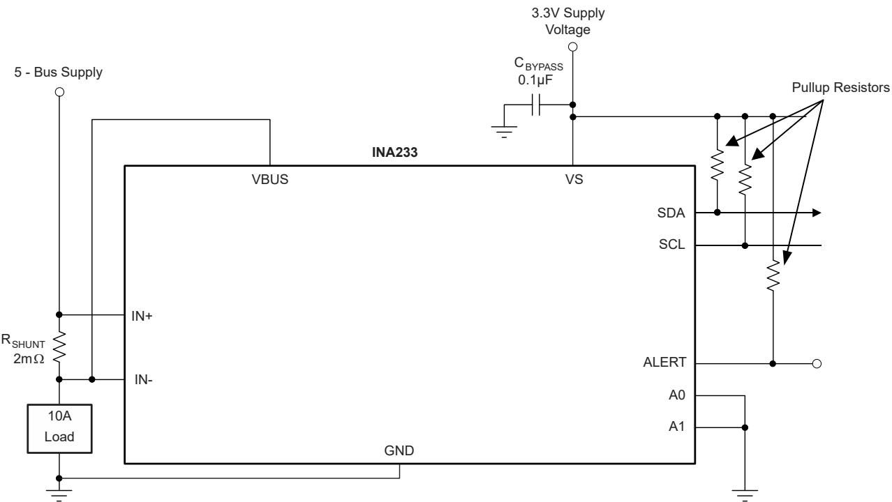
Figure 7-1. Typical High-Side Sensing Circuit Configuration, INA233
7.2.1 Design Requirements
The INA233 measures the voltage developed across a current-sensing resistor $( \mathsf { R } _ { \mathsf { S H U N T } } )$ when current passes through the resistor. The device also measures the bus supply voltage and can calculate power when the calibration register is properly configured. The device comes with alert capability where the ALERT pin can be programmed to respond to a user-defined event or to a conversion ready notification. This design illustrates the ability of the ALERT pin to respond to a set input overvoltage threshold and how to correctly set the calibration registers and calculate returned values. Table 7-1 details the requirements for this design.
Table 7-1. Design Requirements
| PARAMETER | DESIGN TARGET |
| Power-supply voltage, $V_S$ | 5V |
| Nominal bus supply voltage, $V_BUS$ | 5V |
| VBUS overvoltage warning threshold | 5.5V |
| Nominal load current | 10A |
| Peak load current | 15A |
| Overcurrent warning threshold | 15A |
| $R_{SHUNT}$ | 2mΩ |
7.2.2 Detailed Design Procedure
This design example walks through the process of programming the calibration register, calculating the PMBus coefficients, setting the correct overvoltage and overcurrent warning thresholds, and how to properly scale returned values from the device. The device alert response time is also examined with 140-µs and 1.1-ms ADC conversion rates.
7.2.2.1 Programming the Calibration Register
For this example, assuming a peak current of less than 15 A, the Current_LSB is calculated to be 457.7 μA/bit using Equation 2. Selecting a value for the Current_LSB of 500 μA/bit or 1 mA/bit significantly simplifies the conversion of the returned value from the READ_IIN and READ_PIN commands to amperes and watts. For this example, a value of 1 mA/bit is chosen for the Current_LSB. Using this value for the Current_LSB does trade a small amount of resolution for having a simpler conversion process on the user side. Using Equation 1 in this example with a Current_LSB value of 1 mA/bit and a shunt resistor of 2 mΩ results in a MFR_CALIBRATION register value of 2560d (or A00h).
7.2.2.2 Calculating PMBus Coefficients
The m, b, and R coefficients are fixed for bus voltage measurements returned by the READ_VIN and READ_VOUT and are available from Table 6-1.
For current and power measurements, the value for the m and R coefficients must be calculated. For current measurements returned by the READ_IIN and READ_IOUT commands, the value for m is calculated by inverting the Current_LSB used to set the MFR_CALIBRATION register and shifting the decimal location if needed to minimize rounding errors. In this example, using the Current_LSB of 1 mA/bit, the value of m is calculated to be 1000. Shifting the decimal location does not obtain higher accuracy because the value for m is a whole number. The value for R in this example is 0 because the decimal location for the value of m does not need shifting.
The POWER_LSB value is 25 times the value of the CURRENT_LSB, therefore, the value for m is reduced by a factor of 25. For this example, the value for the m power coefficient 1000 / 25 or 40. For this case, the R coefficient is also 0 because m is a whole number. If m is not a whole number, then shifting the decimal place is advantageous to reduce rounding errors while keeping the value between –32768 and 32767. Decimal shifts to the right result in negative values for R and shifts to the left result in positive values; the number of shifts is the absolute value of R.
The value of 0 can be used for b for both current and power measurements with very little loss in accuracy because the offset for power and current measurements is very low. The m, b, and R coefficients are fixed for bus voltage measurements returned by the READ_VIN and READ_VOUT and are available from Table 6-1.
7.2.2.3 Programming Warning Thresholds
Warning thresholds are set by converting the warning value from volts, amperes, and watts to the appropriate digital word using Equation 4 with the correct values for m, b, and R. For example, to set a bus voltage overvoltage warning at 5.5 V with the VIN_OV_WARN_LIMIT command, the correct value to write with this command is 4400d or 1130h. The least significant last three bits of the 16-bit word are hard coded to 0 because the warning thresholds only have 12 bits of effective resolution. For this example there is no change to what is written in the VIN_OV_WARN_LIMIT register because the last three bits are already zero. To set an overcurrent warning level at 15 A with the IIN_OC_WARN_LIMIT command, the correct value to write to the device is 15000d (or 3A98h).
7.2.2.4 Calculating Returned Telemetry Values
When the value for the m, b, and R coefficients are known, returned values can be translated to volts, amperes, or watts by using Equation 3 with the calculated m, b, and R coefficients. Alternatively, returned values can be calculated by multiplying the returned code by the corresponding LSB size as discussed in the Calibration Register and Scaling section.
7.2.3 Application Curves
Figure 7-2 shows the ALERT pin response to a bus overvoltage limit of 5.6V for a conversion time (tCT) of 1.1ms and averaging set to 1. Figure 7-3 shows the response for the same limit but with the conversion time reduced to 140µs. For the scope shots shown in these figures, persistence is enabled on the ALERT channel. Figure 7-2 and Figure 7-3 show how the ALERT response time can vary depending on when the fault condition occurs relative to the internal ADC clock of the INA233. For fault conditions that are just exceeding the limit threshold, the response time for the ALERT pin can vary from one to two conversion cycles. As mentioned previously, the variation is because of the timing on when the fault event occurs relative to the start time of the internal ADC conversion cycle. For fault events that greatly exceed the limit threshold, the alert can respond in less than one conversion cycle because fewer samples are required for the average to exceed the limit threshold value.
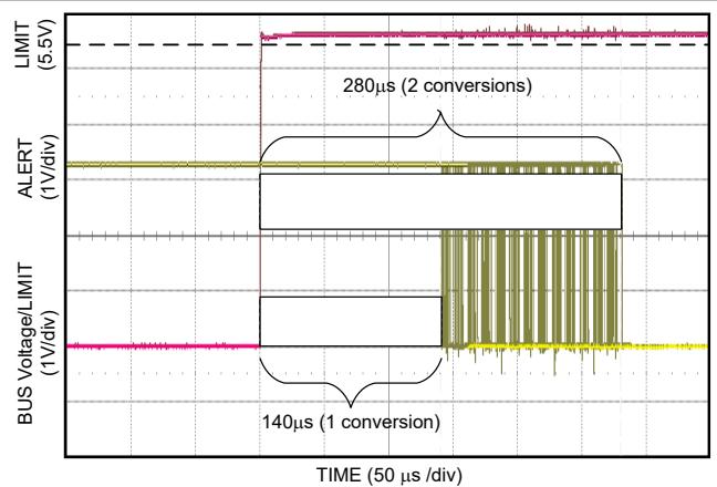
Figure 7-2. Alert Response $( \mathtt { t _ { C T } } = 1 4 0 \mu \mathsf { s } )$

Figure 7-3. Alert Response (tCT = 1.1ms)
7.3 Power Supply Recommendations
The device input circuitry can accurately measure signals on common-mode voltages beyond the power-supply voltage, $\mathsf { V } _ { \mathsf { V S } }$ . For example, the voltage applied to the VS power supply pin can be 5V, whereas the load power-supply voltage being monitored (the common-mode voltage) can be as high as 36V. The device can also withstand the full 0V to 36V range at the input pins, regardless of whether the device has power applied or not.
Place the required power-supply bypass capacitors as close as possible to the supply and ground pins of the device to provide stability. A typical value for this supply bypass capacitor is 0.1µF. Applications with noisy or high-impedance power supplies can require additional decoupling capacitors to reject power-supply noise.
7.4 Layout
7.4.1 Layout Guidelines
Connect the input pins (IN+ and IN–) to the sensing resistor using a Kelvin connection or a 4-wire connection. These connection techniques verify that only the current-sensing resistor impedance is detected between the input pins. Poor routing of the current-sensing resistor commonly results in additional resistance present between the input pins. Given the very low ohmic value of the current-sensing resistor, any additional highcurrent carrying impedance causes significant measurement errors. Place the power-supply bypass capacitor as close as possible to the supply and ground pins.
7.4.2 Layout Example

A. Connect the VBUS pin to the power-supply rail.
Figure 7-4. INA233 Layout Example
8 Device and Documentation Support
8.1 Device Support
8.1.1 Development Support
• Texas Instruments, INA226EVM Evaluation Board and Software Tutorial user's guide
8.2 Documentation Support
8.2.1 Related Documentation
For related documentation see the following:
Texas Instruments, Current Shunt Monitor with Transient Robustness reference design
8.3 Receiving Notification of Documentation Updates
To receive notification of documentation updates, navigate to the device product folder on ti.com. Click on Notifications to register and receive a weekly digest of any product information that has changed. For change details, review the revision history included in any revised document.
8.4 Support Resources
TI E2E™ support forums are an engineer's go-to source for fast, verified answers and design help — straight from the experts. Search existing answers or ask your own question to get the quick design help you need.
Linked content is provided "AS IS" by the respective contributors. They do not constitute TI specifications and do not necessarily reflect TI's views; see TI's Terms of Use.
8.5 Trademarks
TI E2E™ is a trademark of Texas Instruments.
All trademarks are the property of their respective owners.
8.6 Electrostatic Discharge Caution

This integrated circuit can be damaged by ESD. Texas Instruments recommends that all integrated circuits be handled with appropriate precautions. Failure to observe proper handling and installation procedures can cause damage.
ESD damage can range from subtle performance degradation to complete device failure. Precision integrated circuits may be more susceptible to damage because very small parametric changes could cause the device not to meet its published specifications.
8.7 Glossary
TI Glossary This glossary lists and explains terms, acronyms, and definitions.
9 Revision History
Changes from Revision * (April 2017) to Revision A (March 2025)
Page
• Updated the numbering format for tables, figures, and cross-references throughout the document................. 1
10 Mechanical, Packaging, and Orderable Information
The following pages include mechanical, packaging, and orderable information. This information is the most current data available for the designated devices. This data is subject to change without notice and revision of this document. For browser-based versions of this data sheet, refer to the left-hand navigation.
PACKAGING INFORMATION
| Orderable part number | Status(1) | Material type(2) | Package | Pins | Package qty | Carrier | RoHS(3) | Lead finish/ Ball material(4) | MSL rating/ Peak reflow(5) | Op temp (°C) | Part marking(6) |
| INA233AIDGSR | Active | Production | VSSOP (DGS) | 10 | 2500 | LARGE T&R | Yes | NIPDAUAG | SN | Level-2-260C-1 YEAR | -40 to 125 | 233 |
| INA233AIDGSR.B | Active | Production | VSSOP (DGS) | 10 | 2500 | LARGE T&R | Yes | SN | Level-2-260C-1 YEAR | -40 to 125 | 233 |
(1) Status: For more details on status, see our product life cycle.
(2) Material type: When designated, preproduction parts are prototypes/experimental devices, and are not yet approved or released for full production. Testing and final process, including without limitation quality assurance, reliability performance testing, and/or process qualification, may not yet be complete, and this item is subject to further changes or possible discontinuation. If available for ordering, purchases will be subject to an additional waiver at checkout, and are intended for early internal evaluation purposes only. These items are sold without warranties of any kind.
(3) RoHS values: Yes, No, RoHS Exempt. See the TI RoHS Statement for additional information and value definition.
(4) Lead finish/Ball material: Parts may have multiple material finish options. Finish options are separated by a vertical ruled line. Lead finish/Ball material values may wrap to two lines if the finish value exceeds the maximum column width.
(5) MSL rating/Peak reflow: The moisture sensitivity level ratings and peak solder (reflow) temperatures. In the event that a part has multiple moisture sensitivity ratings, only the lowest level per JEDEC standards is shown. Refer to the shipping label for the actual reflow temperature that will be used to mount the part to the printed circuit board.
(6) Part marking: There may be an additional marking, which relates to the logo, the lot trace code information, or the environmental category of the part.
Multiple part markings will be inside parentheses. Only one part marking contained in parentheses and separated by a "~" will appear on a part. If a line is indented then it is a continuation of the previous line and the two combined represent the entire part marking for that device.
Important Information and Disclaimer:The information provided on this page represents TI's knowledge and belief as of the date that it is provided. TI bases its knowledge and belief on information provided by third parties, and makes no representation or warranty as to the accuracy of such information. Efforts are underway to better integrate information from third parties. TI has taken and continues to take reasonable steps to provide representativ and accurate information but may not have conducted destructive testing or chemical analysis on incoming materials and chemicals. TI and TI suppliers consider certain information to be proprietary, and thus CAS number and other limited information may not be available for release.
In no event shall TI's liability arising out of such information exceed the total purchase price of the TI part(s) at issue in this document sold by TI to Customer on an annual basis.
TAPE AND REEL INFORMATION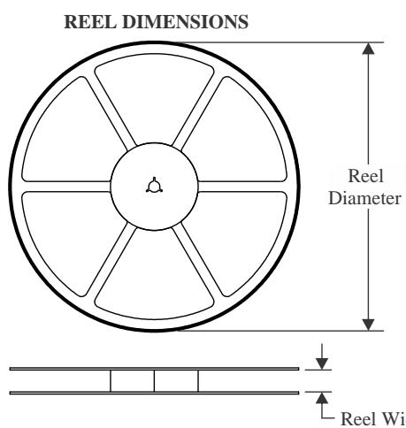
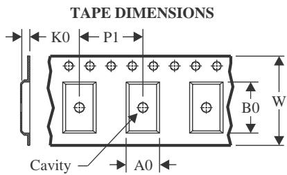
| A0 | Dimension designed to accommodate the component width |
| B0 | Dimension designed to accommodate the component length |
| K0 | Dimension designed to accommodate the component thickness |
| W | Overall width of the carrier tape |
| P1 | Pitch between successive cavity centers |
Reel Width (W1)
QUADRANT ASSIGNMENTS FOR PIN 1 ORIENTATION IN TAPE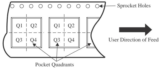
*All dimensions are nomina
| Device | Package Type | Package Drawing | Pins | SPQ | Reel Diameter (mm) | Reel Width W1 (mm) | A0 (mm) | B0 (mm) | K0 (mm) | P1 (mm) | W (mm) | Pin1 Quadrant |
| INA233AIDGSR | VSSOP | DGS | 10 | 2500 | 330.0 | 12.4 | 5.25 | 3.35 | 1.25 | 8.0 | 12.0 | Q1 |
*All dimensions are nominal
| Device | Package Type | Package Drawing | Pins | SPQ | Length (mm) | Width (mm) | Height (mm) |
| INA233AIDGSR | VSSOP | DGS | 10 | 2500 | 366.0 | 364.0 | 50.0 |
SMALL OUTLINE PACKAGE

NOTES:
All linear dimensions are in millimeters. Any dimensions in parenthesis are for reference only. Dimensioning and tolerancing per ASME Y14.5M.
This drawing is subject to change without notice.
This dimension does not include mold flash, protrusions, or gate burrs. Mold flash, protrusions, or gate burrs shall not exceed 0.15 mm per side.
SMALL OUTLINE PACKAGE

NOTES: (continued)
4221984/A 05/2015
Publication IPC-7351 may have alternate designs.
Solder mask tolerances between and around signal pads can vary based on board fabrication site.
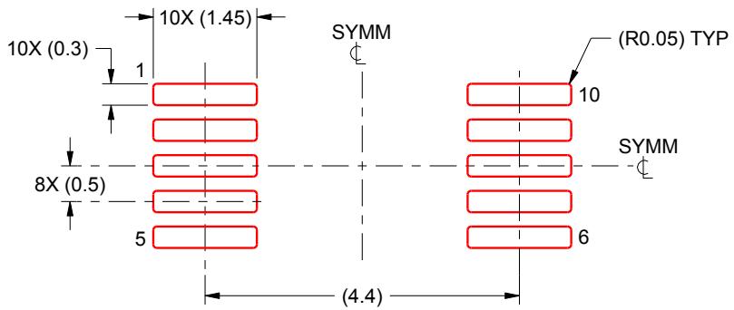
SOLDER PASTE EXAMPLE BASED ON 0.125 mm THICK STENCIL SCALE:10X
4221984/A 05/2015
NOTES: (continued)
Laser cutting apertures with trapezoidal walls and rounded corners may offer better paste release. IPC-7525 may have alternate design recommendations.
Board assembly site may have different recommendations for stencil design.
Figures and diagrams from the PDF
Preview the extracted datasheet assets and open any image in a separate tab for closer inspection.


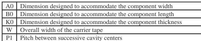
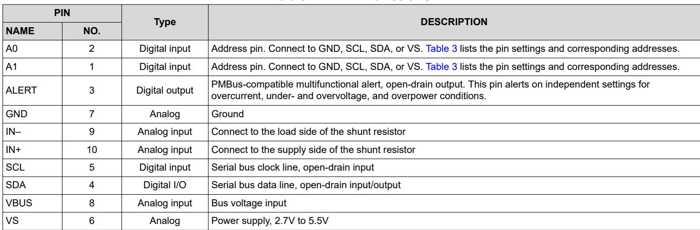
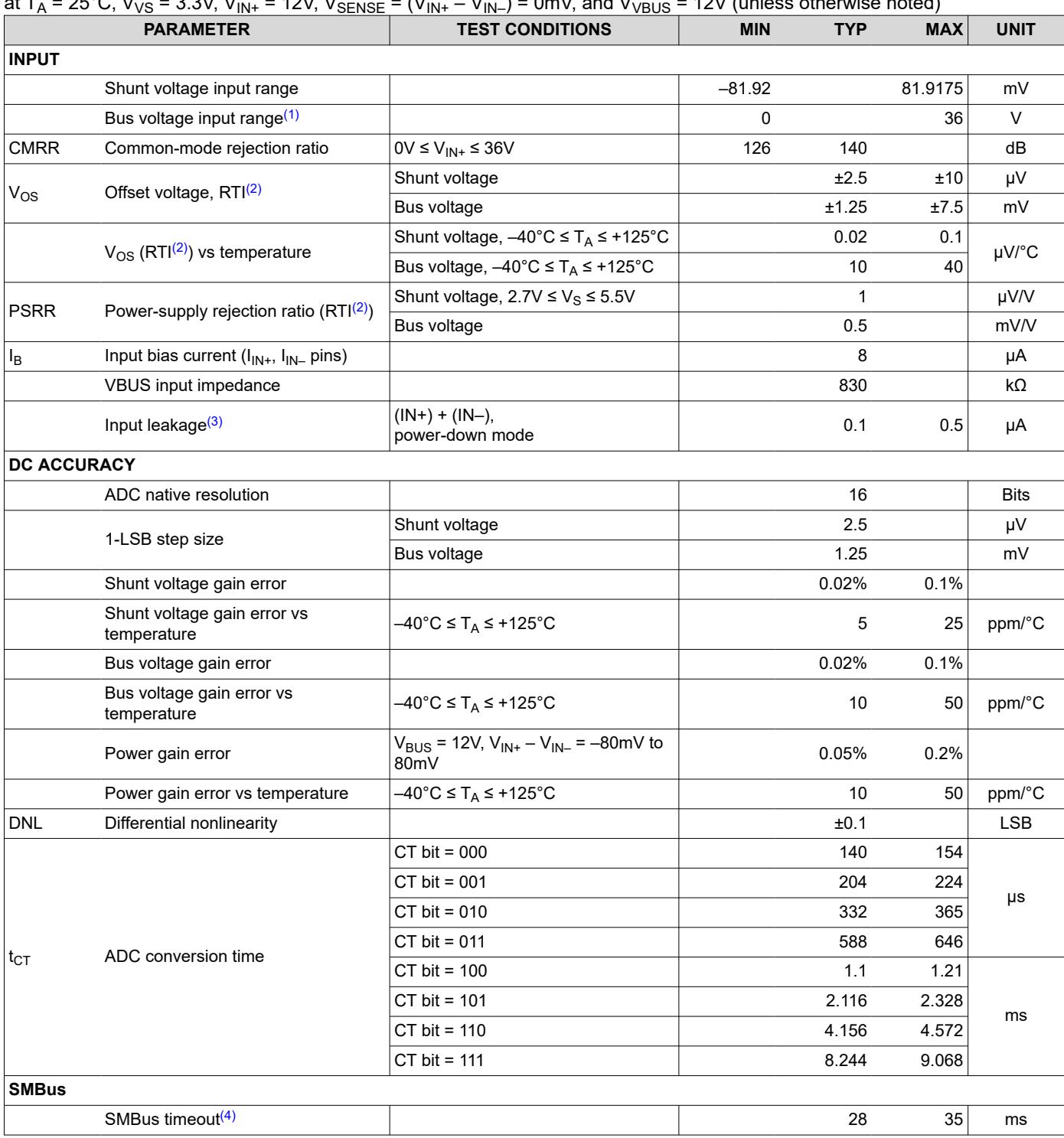
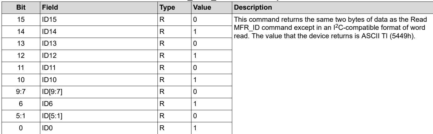

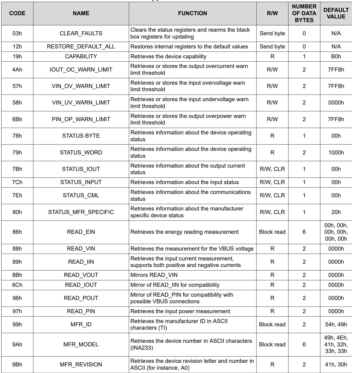

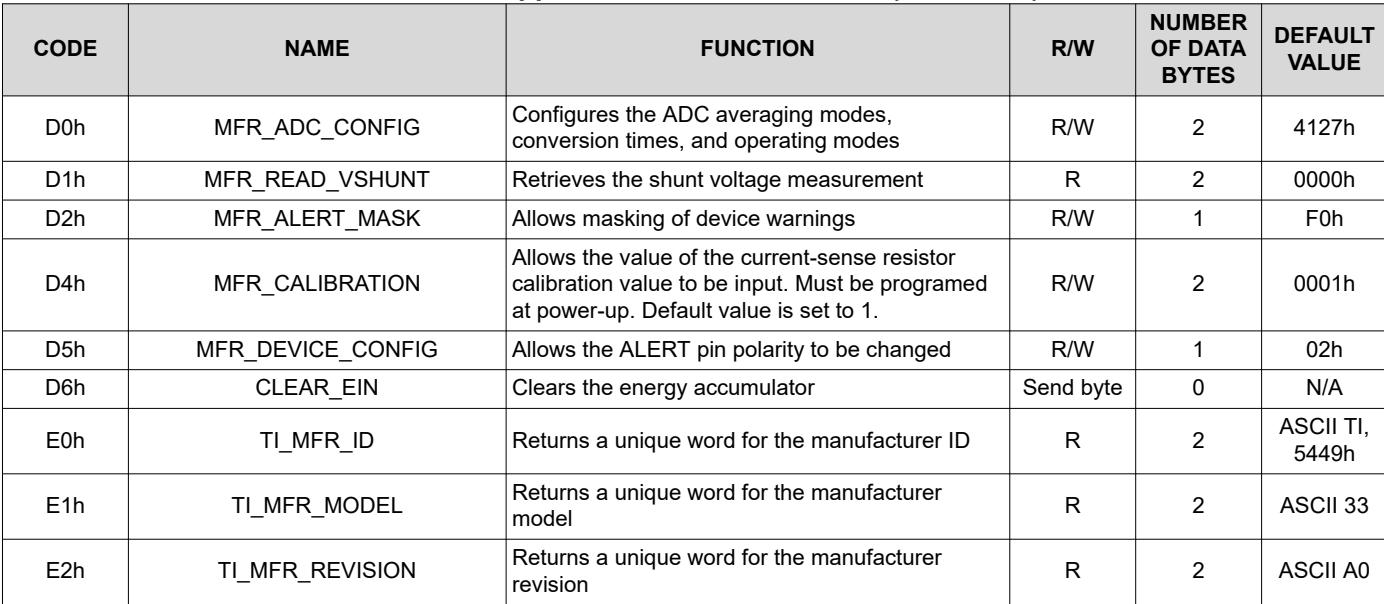
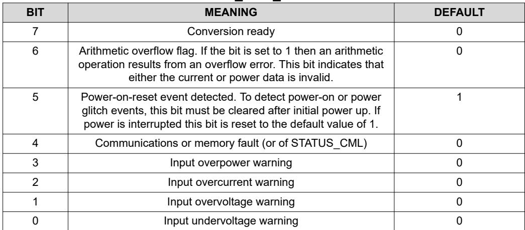



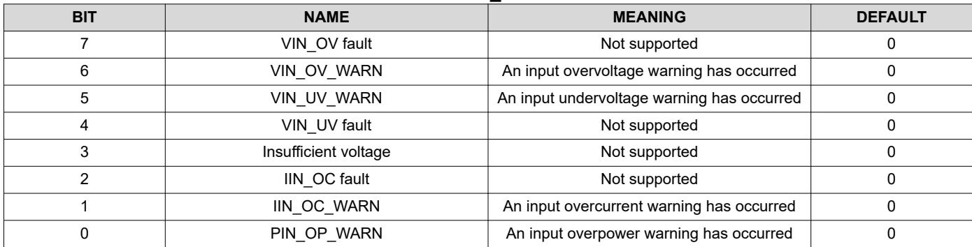
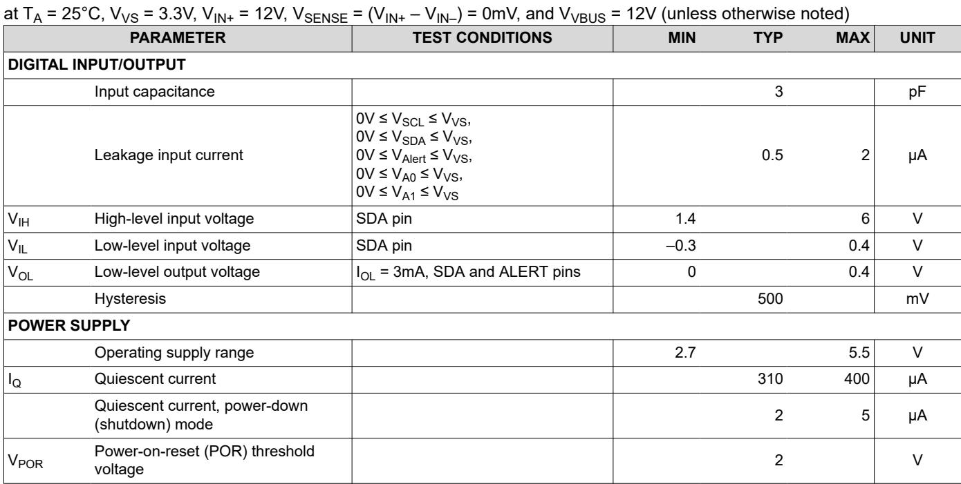

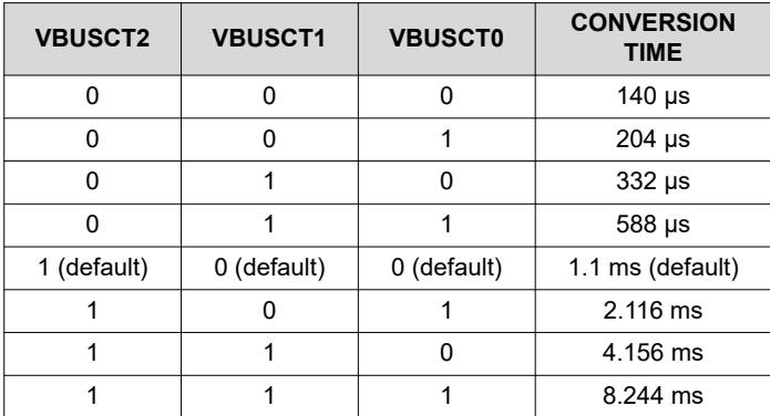


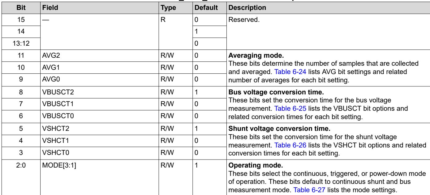
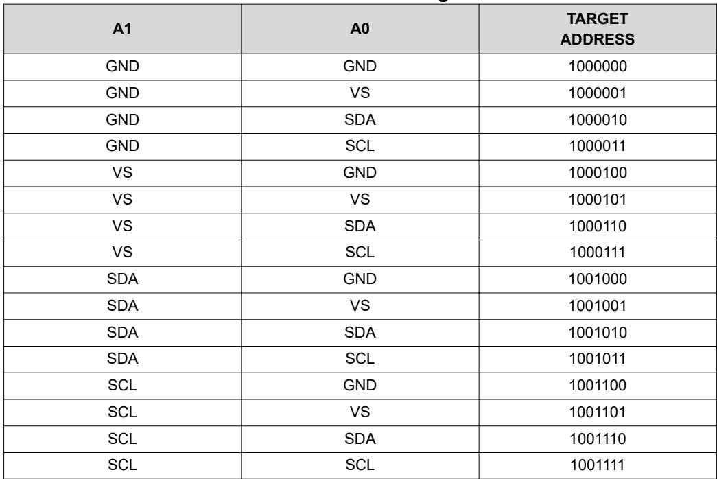

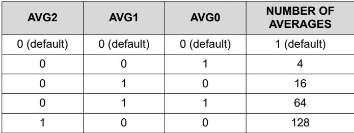



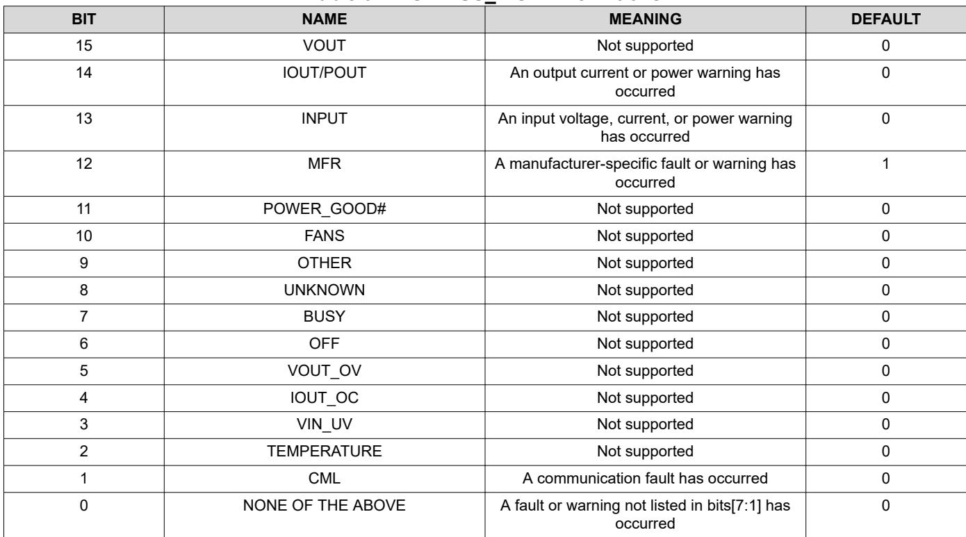
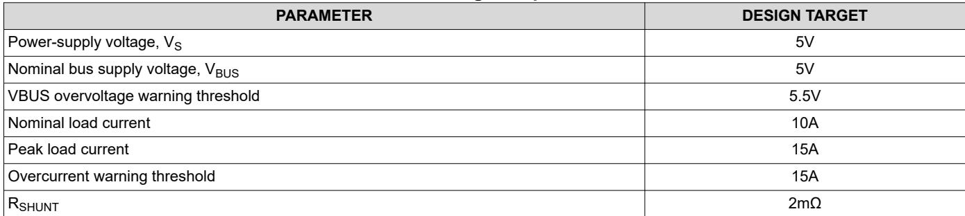

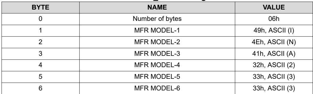
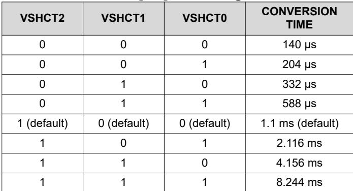

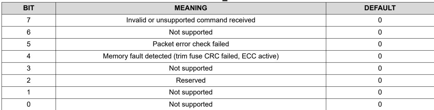
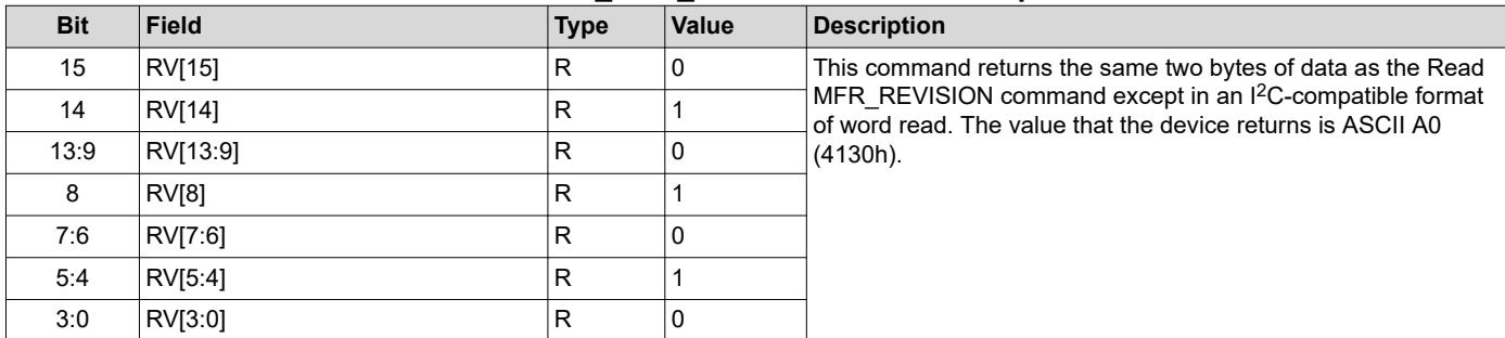

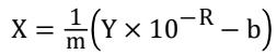
Use this datasheet from any agent
Send the page, markdown, chunks, or search endpoint to ChatGPT, Claude, embedr-app, or your own tooling.