
LTC2990 Quad I2C Voltage, Current and Temperature Monitor
14-bit monitor IC for measuring voltage, current, internal temperature, and two remote diode temperatures.
Quad $^ { 1 2 } \mathsf { C }$ Voltage, Current and Temperature Monitor
FEATURES
n Measures Voltage, Current and Temperature
n Measures Two Remote Diode Temperatures
n $\pm 0 . 5 %$ Accuracy, $0 . 0 6 ^ { \circ } C$ Resolution (Typ)
n $\pm 1 %$ Internal Temperature Sensor (Typ)
n 14-Bit ADC Measures Voltage/Current
n 3V to 5.5V Supply Operating Voltage
n Four Selectable Addresses
n Internal $1 0 0 \mathsf { { p m } } / \mathsf { { ^ o C } }$ Voltage Reference
n 10-Lead MSOP Package
APPLICATIONS
n Temperature Measurement
n Supply Voltage Monitoring
n Current Measurement
n Remote Data Acquisition
n Environmental Monitoring
TYPICAL APPLICATION
Voltage, Current, Temperature Monitor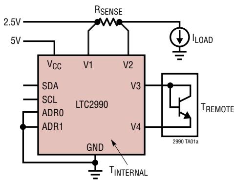
MEASURES: TWO SUPPLY VOLTAGES,SUPPLY CURRENT, INTERNAL ANDREMOTE TEMPERATURES
DESCRIPTION
The LTC®2990 is used to monitor system temperatures, voltages and currents. Through the $| ^ { 2 } 0$ serial interface, the device can be configured to measure many combinations of internal temperature, remote temperature, remote voltage, remote current and internal $\mathsf { V } _ { \mathsf { C C } }$ . The internal $1 0 0 \mathsf { p m / ^ { \circ } C }$ reference minimizes the number of supporting components and area required. Selectable address and configurable functionality give the LTC2990 flexibility to be incorporated in various systems needing temperature, voltage or current data. The LTC2990 fits well in systems needing sub-millivolt voltage resolution, $1 %$ current measurement and $1 %$ temperature accuracy or any combination of the three.
ABSOLUTE MAXIMUM RATINGS
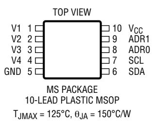
PIN CONFIGURATION
(Note 1) Supply Voltage VCC ......... . –0.3V to 6.0V Input Voltages V1, V2, V3, V4, SDA, SCL, ADR1, ADR2... ...–0.3V to (VCC + 0.3V) Operating Temperature Range LTC2990C.. . 0°C to 70°C LTC2990I .. .–40°C to 85°C Storage Temperature Range ........ ... –65°C to 150°C Lead Temperature (Soldering, 10 sec)................... 300°C
ORDER INFORMATION
| LEAD FREE FINISH | TAPE AND REEL | PART MARKING* | PACKAGE DESCRIPTION | TEMPERATURE RANGE |
| LTC2990CMS#PBF | LTC2990CMS#TRPBF | LTDSQ | 10-Lead Plastic MSOP | 0°C to 70°C |
| LTC2990IMS#PBF | LTC2990IMS#TRPBF | LTDSQ | 10-Lead Plastic MSOP | -40°C to 85°C |
| LEAD BASED FINISH | TAPE AND REEL | PART MARKING* | PACKAGE DESCRIPTION | TEMPERATURE RANGE |
| LTC2990CMS | LTC2990CMS#TR | LTDSQ | 10-Lead Plastic MSOP | 0°C to 70°C |
| LTC2990IMS | LTC2990IMS#TR | LTDSQ | 10-Lead Plastic MSOP | -40°C to 85°C |
Consult the factory for parts specified with wider operating temperature ranges. *The temperature grade is identified by a label on the shipping container. Contact the factory for parts trimmed to ideality factors other than 1.004.
Tape and reel specifications. Some packages are available in 500 unit reels through designated sales channels with #TRMPBF suffix.
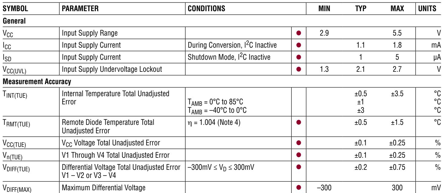
ELECTRICAL CHARACTERISTICS The l denotes the specifications which apply over the full operating temperature range, otherwise specifications are at TA = 25°C. VCC = 3.3V, unless otherwise noted.
| SYMBOL | PARAMETER | CONDITIONS | MIN | TYP | MAX | UNITS | |
| General | |||||||
| $V_{CC}$ | Input Supply Range | ● | 2.9 | 5.5 | V | ||
| $I_{CC}$ | Input Supply Current | During Conversion, $I^{2}C$ Inactive | ● | 1.1 | 1.8 | mA | |
| $I_{SD}$ | Input Supply Current | Shutdown Mode, $I^{2}C$ Inactive | ● | 1 | 5 | μA | |
| $V_{CC(UVL)}$ | Input Supply Undervoltage Lockout | ● | 1.3 | 2.1 | 2.7 | V | |
| Measurement Accuracy | |||||||
| $T_{INT(TUE)}$ | Internal Temperature Total Unadjusted Error | $T_{AMB}=0°C to 85°C$ $T_{AMB}=-40°C to 0°C$ | ±0.5±1±3 | ±3.5 | °C°C°C | ||
| $T_{RMT(TUE)}$ | Remote Diode Temperature Total Unadjusted Error | η=1.004 (Note 4) | ● | ±0.5 | ±1.5 | °C | |
| $V_{CC(TUE)}$ | $V_{CC}$ Voltage Total Unadjusted Error | ● | ±0.1 | ±0.25 | % | ||
| $V_{n(TUE)}$ | V1 Through V4 Total Unadjusted Error | ● | ±0.1 | ±0.25 | % | ||
| $V_{DIFF(TUE)}$ | Differential Voltage Total Unadjusted Error V1-V2 or V3-V4 | -300mV ≤ $V_D$ ≤ 300mV | ● | ±0.2 | ±0.75 | % | |
| $V_{DIFF(MAX)}$ | Maximum Differential Voltage | ● | -300 | 300 | mV | ||
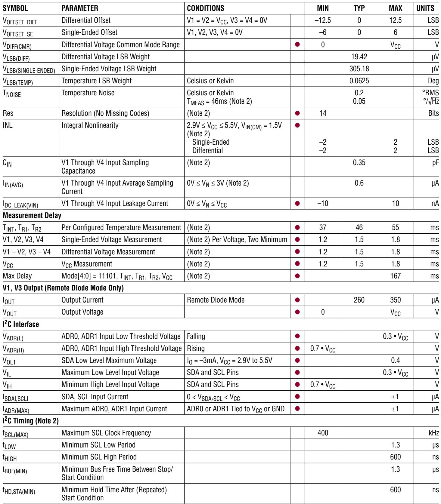
ELECTRICAL CHARACTERISTICS The l denotes the specifications which apply over the full operating temperature range, otherwise specifications are at $\mathsf { T } _ { \mathsf { A } } = 2 5 ^ { \circ } \mathsf { C } . \mathsf { V } _ { \mathsf { C C } } = 3 . 3 \mathsf { V }$ , unless otherwise noted.
| SYMBOL | PARAMETER | CONDITIONS | MIN | TYP | MAX | UNITS | |
| $V_{OFFSET\_DIFF}$ | Differential Offset | V1 = V2 = $V_{CC}$ , V3 = V4 = 0V | -12.5 | 0 | 12.5 | LSB | |
| $V_{OFFSET\_SE}$ | Single-Ended Offset | V1, V2, V3, V4 = 0V | -6 | 0 | 6 | LSB | |
| $V_{DIFF(CMR)}$ | Differential Voltage Common Mode Range | ● | 0 | $V_{CC}$ | V | ||
| $V_{LSB(DIFF)}$ | Differential Voltage LSB Weight | 19.42 | μV | ||||
| $V_{LSB(SINGLE-ENDED)}$ | Single-Ended Voltage LSB Weight | 305.18 | μV | ||||
| $V_{LSB(TEMP)}$ | Temperature LSB Weight | Celsius or Kelvin | 0.0625 | Deg | |||
| $T_{NOISE}$ | Temperature Noise | Celsius or Kelvin $T_{MEAS} = 46ms (Note 2)$ | 0.20.05 | °RMS°/√Hz | |||
| Res | Resolution (No Missing Codes) | (Note 2) | ● | 14 | Bits | ||
| INL | Integral Nonlinearity | 2.9V ≤ $V_{CC}$ ≤ 5.5V, $V_{IN(CM)}$ = 1.5V(Note 2)Single-Ended Differential | -2-2 | 22 | LSBLSB | ||
| $C_{IN}$ | V1 Through V4 Input Sampling Capacitance | (Note 2) | 0.35 | pF | |||
| $I_{IN(AVG)}$ | V1 Through V4 Input Average Sampling Current | 0V ≤ $V_N$ ≤ 3V (Note 2) | 0.6 | μA | |||
| $I_{DC\_LEAK(VIN)}$ | V1 Through V4 Input Leakage Current | 0V ≤ $V_N$ ≤ $V_{CC}$ | ● | -10 | 10 | nA | |
| Measurement Delay | |||||||
| $T_{INT}, T_{R1}, T_{R2}$ | Per Configured Temperature Measurement | (Note 2) | ● | 37 | 46 | 55 | ms |
| V1, V2, V3, V4 | Single-Ended Voltage Measurement | (Note 2) Per Voltage, Two Minimum | ● | 1.2 | 1.5 | 1.8 | ms |
| V1 - V2, V3 - V4 | Differential Voltage Measurement | (Note 2) | ● | 1.2 | 1.5 | 1.8 | ms |
| $V_{CC}$ | $V_{CC}$ Measurement | (Note 2) | ● | 1.2 | 1.5 | 1.8 | ms |
| Max Delay | Mode[4:0] = 11101, $T_{INT}, T_{R1}, T_{R2}, V_{CC}$ | (Note 2) | ● | 167 | ms | ||
| V1, V3 Output (Remote Diode Mode Only) | |||||||
| $I_{OUT}$ | Output Current | Remote Diode Mode | ● | 260 | 350 | μA | |
| $V_{OUT}$ | Output Voltage | ● | 0 | $V_{CC}$ | V | ||
| $I^{2}C Interface$ | |||||||
| $V_{ADR(L)}$ | ADRO, ADR1 Input Low Threshold Voltage | Falling | ● | 0.3 • $V_{CC}$ | V | ||
| $V_{ADR(H)}$ | ADRO, ADR1 Input High Threshold Voltage | Rising | ● | 0.7 • $V_{CC}$ | V | ||
| $V_{OL1}$ | SDA Low Level Maximum Voltage | $I_O$ = -3mA, $V_{CC}$ = 2.9V to 5.5V | ● | 0.4 | V | ||
| $V_{IL}$ | Maximum Low Level Input Voltage | SDA and SCL Pins | ● | 0.3 • $V_{CC}$ | V | ||
| $V_{IH}$ | Minimum High Level Input Voltage | SDA and SCL Pins | ● | 0.7 • $V_{CC}$ | V | ||
| $I_{SDAI,SCLI}$ | SDA, SCL Input Current | 0 < $V_{SDA,SCL} < V_{CC}$ | ● | ±1 | μA | ||
| $I_{ADR(MAX)}$ | Maximum ADR0, ADR1 Input Current | ADRO or ADR1 Tied to $V_{CC}$ or GND | ● | ±1 | μA | ||
| $I^{2}C Timing (Note 2)$ | |||||||
| $f_{SCL(MAX)}$ | Maximum SCL Clock Frequency | 400 | kHz | ||||
| $t_{LOW}$ | Minimum SCL Low Period | 1.3 | μs | ||||
| $t_{HIGH}$ | Minimum SCL High Period | 600 | ns | ||||
| $t_{BUF(MIN)}$ | Minimum Bus Free Time Between Stop/Start Condition | 1.3 | μs | ||||
| $t_{HD,STA(MIN)}$ | Minimum Hold Time After (Repeated) Start Condition | 600 | ns | ||||
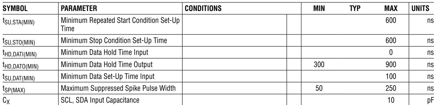
ELECTRICAL CHARACTERISTICS The l denotes the specifications which apply over the full operating temperature range, otherwise specifications are at $\mathsf { T } _ { \mathsf { A } } = 2 5 ^ { \circ } \mathsf { C } . \mathsf { V } _ { \mathsf { C C } } = 3 . 3 \mathsf { V }$ , unless otherwise noted.
| SYMBOL | PARAMETER | CONDITIONS | MIN | TYP | MAX | UNITS | |
| $t_{SU,STA(MIN)}$ | Minimum Repeated Start Condition Set-Up Time | 600 | ns | ||||
| $t_{SU,STO(MIN)}$ | Minimum Stop Condition Set-Up Time | 600 | ns | ||||
| $t_{HD,DATI(MIN)}$ | Minimum Data Hold Time Input | 0 | ns | ||||
| $t_{HD,DATO(MIN)}$ | Minimum Data Hold Time Output | 300 | 900 | ns | |||
| $t_{SU,DAT(MIN)}$ | Minimum Data Set-Up Time Input | 100 | ns | ||||
| $t_{SP(MAX)}$ | Maximum Suppressed Spike Pulse Width | 50 | 250 | ns | |||
| $C_X$ | SCL, SDA Input Capacitance | 10 | pF | ||||
Note 1: Stresses beyond those listed under Absolute Maximum Ratings may cause permanent damage to the device. Exposure to any Absolute Maximum Rating condition for extended periods may affect device reliability and lifetime.
Note 2: Guaranteed by design and not subject to test.
Note 3: Integral nonlinearity is defined as the deviation of a code from a straight line passing through the actual endpoints of the transfer curve. The deviation is measured from the center of the quantization band.
Note 4: Trimmed to an ideality factor of 1.004 at 25°C. Remote diode temperature drift (TUE) verified at diode voltages corresponding to the temperature extremes with the LTC2990 at 25°C. Remote diode temperature drift (TUE) guaranteed by characterization over the LTC2990 operating temperature range.
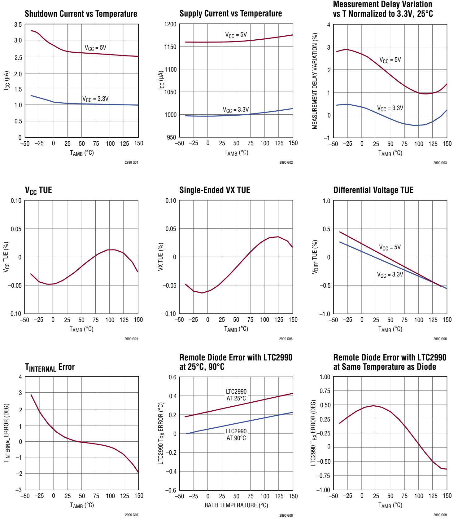
TYPICAL PERFORMANCE CHARACTERISTICS $T _ { A } = 2 5 ^ { \circ } \ell ,$ $\mathtt { V } _ { \mathtt { C } \mathtt { C } } = 3 . 3 \mathtt { V }$ unless otherwise noted
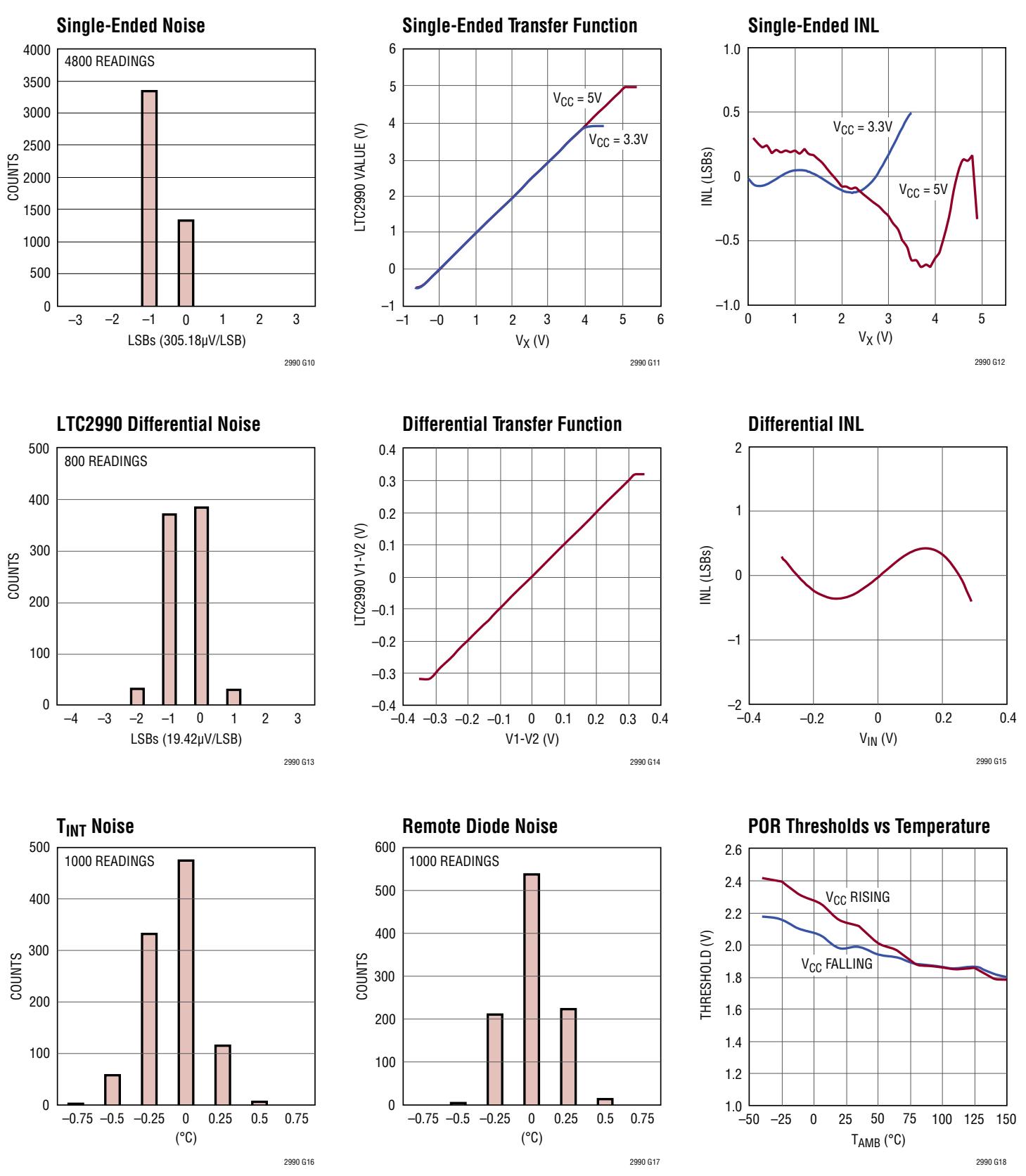
TYPICAL PERFORMANCE CHARACTERISTICS $\mathsf { T } _ { \mathsf { A } } = 2 5 ^ { \circ } \mathsf { C } , \mathsf { V } _ { \mathsf { C C } } = 3 . 3 \mathsf { V }$ unless otherwise noted
PIN FUNCTIONS
V1 (Pin 1): First Monitor Input. This pin can be configured as a single-ended input or the positive input for a differential or remote diode temperature measurement (in combination with V2). When configured for remote diode temperature, this pin will source a current.
V2 (Pin 2): Second Monitor Input. This pin can be configured as a single-ended input or the negative input for a differential or remote diode temperature measurement (in combination with V1). When configured for remote diode temperature, this pin will have an internal termination, while the measurement is active.
V3 (Pin 3): Third Monitor Input. This pin can be configured as a single-ended input or the positive input for a differential or remote diode temperature measurement (in combination with V4). When configured for remote diode temperature, this pin will source a current.
V4 (Pin 4): Fourth Monitor Input. This pin can be configured as a single-ended input or the negative input for a differential or remote diode temperature measurement (in combination with V3). When configured for remote diode temperature, this pin will have an internal termination, while the measurement is active.
GND (Pin 5): Device Circuit Ground. Connect this pin to a ground plane through a low impedance connection.
SDA (Pin 6): Serial Bus Data Input and Output. In the transmitter mode (Read), the conversion result is output through the SDA pin, while in the receiver mode (Write), the device configuration bits are input through the SDA pin. At data input mode, the pin is high impedance; while at data output mode, it is an open-drain N-channel driver and therefore an external pull-up resistor or current source to VCC is needed.
SCL (Pin 7): Serial Bus Clock Input. The LTC2990 can only act as a slave and the SCL pin only accepts external serial clock. The LTC2990 does not implement clock stretching.
ADR0 (Pin 8): Serial Bus Address Control Input. The ADR0 pin is an address control bit for the device I2C address. See Table 2.
ADR1 (Pin 9): Serial Bus Address Control Input. The ADR1 pin is an address control bit for the device I2C address. See Table 2.
VCC (Pin 10): Supply Voltage Input.
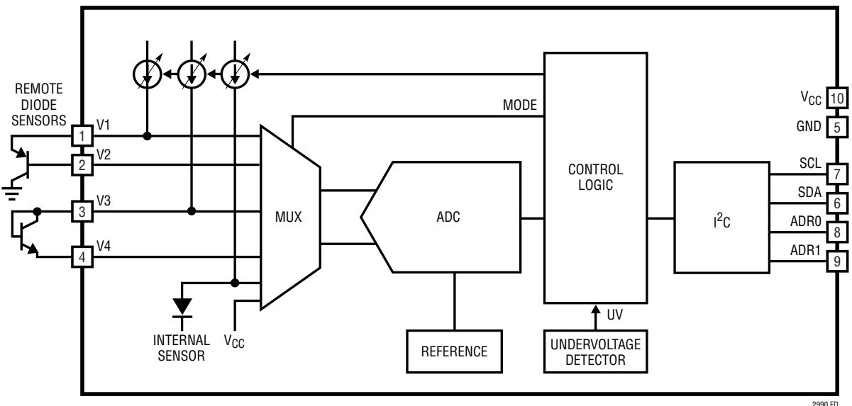
FUNCTIONAL DIAGRAM
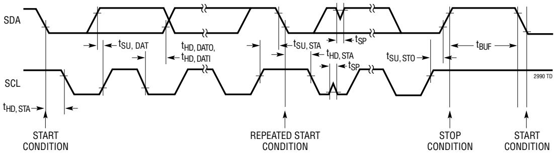
TIMING DIAGRAM
OPERATION
The LTC2990 monitors voltage, current, internal and remote temperatures. It can be configured through an $\mathsf { I 2 0 }$ interface to measure many combinations of these parameters. Single or repeated measurements are possible. Remote temperature measurements use a transistor as a temperature sensor, allowing the remote sensor to be a discrete NPN (ex. MMBT3904) or an embedded PNP device in a microprocessor or FPGA. The internal ADC reference minimizes the number of support components required.
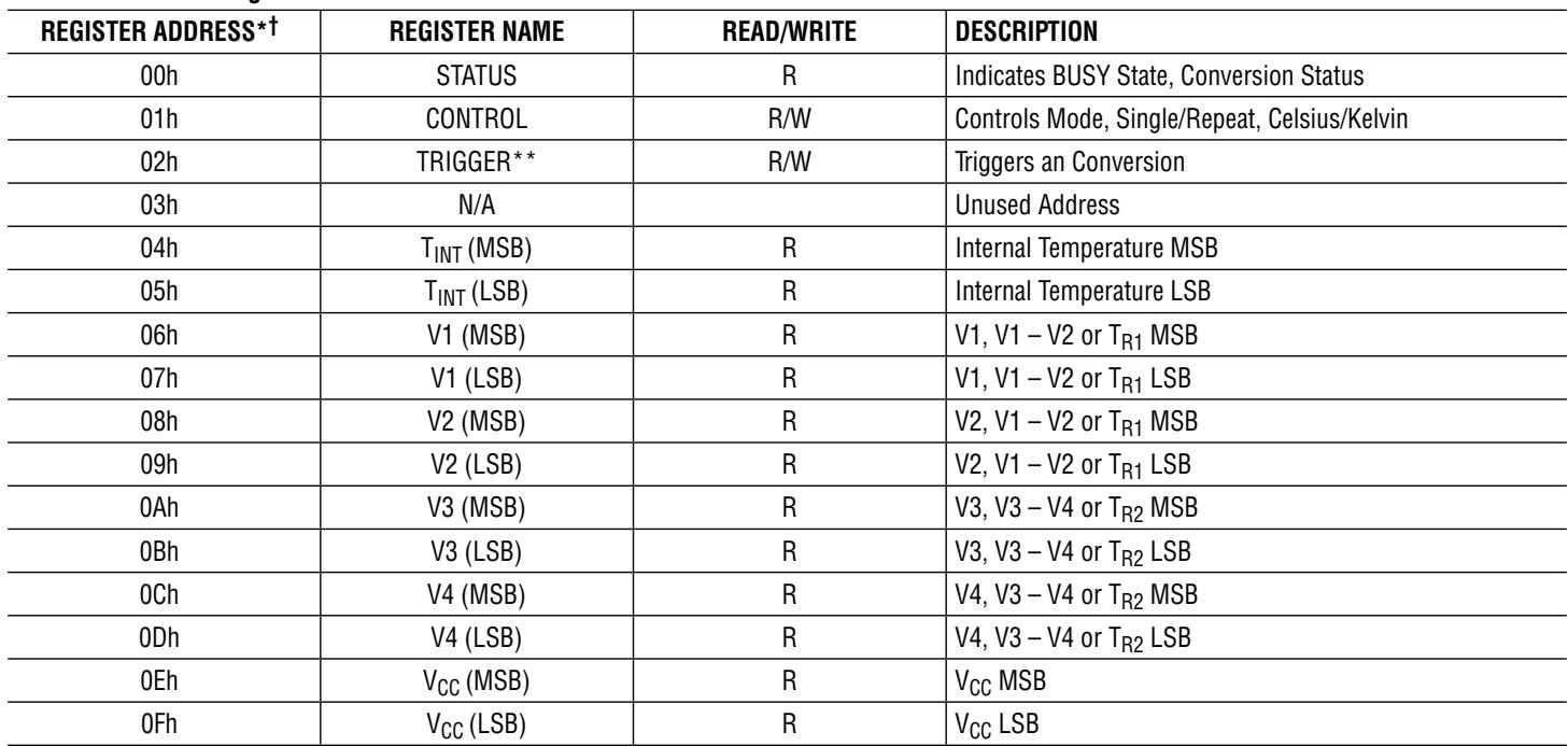
The Functional Diagram displays the main components of the device. The input signals are selected with an input MUX, controlled by the control logic block. The control logic uses the mode bits in the control register to manage the sequence and types of data acquisition. The control logic also controls the variable current sources during remote temperature acquisition. The order of acquisitions is fixed: TINTERNAL, V1, V2, V3, V4 then $\mathsf { V } _ { \mathsf { C C } }$ . The ADC performs the necessary conversion(s) and supplies the data to the control logic for further processing in the case of temperature measurements, or routing to the appropriate data register for voltage and current measurements. Current and temperature measurements, V1 – V2 or V3 $- \lor 4$ , are sampled differentially by the internal ADC. The $| 2 0 \rangle$ interface supplies access to control, status and data registers. The ADR1 and ADR0 pins select one of four possible $\mathsf { I 2 0 }$ addresses (see Table 2). The undervoltage
APPLICATIONS INFORMATION
Figure 1 is the basic LTC2990 application circuit.
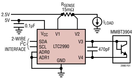
Figure 1.
detector inhibits $| ^ { 2 } 0$ communication below the specified threshold. During an undervoltage condition, the part is in a reset state, and the data and control registers are placed in the default state of 00h.
Remote diode measurements are conducted using multiple ADC conversions and source currents to compensate for sensor series resistance. During temperature measurements, the V2 or V4 terminal of the LTC2990 is terminated with a diode. The LTC2990 is calibrated to yield the correct temperature for a remote diode with an ideality factor of 1.004. See the applications section for compensation of sensor ideality factors other than the factory calibrated value of 1.004.
The LTC2990 communicates through an $| ^ { 2 } 0$ serial interface. The serial interface provides access to control, status and data registers. $| ^ { \dot { 2 } } 0$ defines a 2-wire open-drain interface supporting multiple slave devices and masters on a single bus. The LTC2990 supports 100kbits/s in the standard mode and up to 400kbit/s in fast mode. The four physical addresses supported are listed in Table 2. The $| \dot { 2 } 0 \dot { }$ interface is used to trigger single conversions, or start repeated conversions by writing to a dedicated trigger register. The data registers contain a destructive-read status bit (data valid), which is used in repeated mode to determine if the register’s contents have been previously read. This bit is set when the register is updated with new data, and cleared when read.
Power Up
The $\mathsf { V } _ { \mathsf { C C } }$ pin must exceed the undervoltage (UV) threshold of 2.5V to keep the LTC2990 out of power-on reset. Power-on reset will clear all of the data registers and the control register.
Temperature Measurements
The LTC2990 can measure internal temperature and up to two external diode or transistor sensors. During temperature conversion, current is sourced through either the V1 or the V3 pin to forward bias the sensing diode. The
APPLICATIONS INFORMATION
change in sensor voltage per degree temperature change is $2 7 5 \mu \ V / { } ^ { \circ } \tau$ , so environmental noise must be kept to a minimum. Recommended shielding and PCB trace considerations are illustrated in Figure 2.
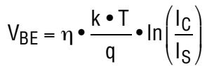
The diode equation:
$$
V _ {B E} = \eta \cdot \frac {k \cdot T}{q} \cdot \ln \left(\frac {I _ {C}}{I _ {S}}\right)\tag{1}
$$
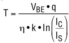
can be solved for T, where T is Kelvin degrees, $| \varsigma$ is a process dependent factor on the order of 1E-13, η is the diode ideality factor, k is Boltzmann’s constant and q is the electron charge.
$$
T = \frac {V _ {B E} \cdot q}{\eta \cdot k \cdot \ln \left(\frac {I _ {C}}{I _ {S}}\right)}\tag{2}
$$
The LTC2990 makes differential measurements of diode voltage to calculate temperature. Proprietary techniques allow for cancellation of error due to series resistance.
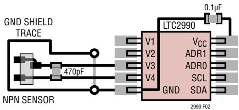
Figure 2. Recommended PCB Layout
Ideality Factor Scaling
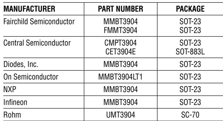
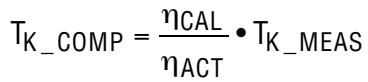
The LTC2990 is factory calibrated for an ideality factor of 1.004, which is typical of the popular MMBT3904 NPN transistor. The semiconductor purity and wafer-level processing limits device-to-device variation, making these devices interchangeable (typically $< 0 . 5 ^ { \circ } \complement )$ for no additional cost. Several manufacturers supply suitable transistors, some recommended sources are listed in Table 1. Discrete 2-terminal diodes are not recommended as temperature sensors. While an ideality factor value of 1.004 is typical of target sensors, small deviations can yield significant temperature errors. Contact LTC Marketing for parts trimmed to ideality factors other than 1.004. The ideality factor of the diode sensor can be considered a temperature scaling factor. The temperature error for a 1% accurate ideality factor error is 1% of the Kelvin temperature. Thus, at $2 5 ^ { \circ } \mathsf C ,$ or 298K, a +1% accurate ideality factor error yields a +2.98 degree error. At $8 5 %$ or 358K, a +1% error yields a 3.6 degree error. It is possible to scale the measured Kelvin or Celsius temperature measured using the LTC2990 with a sensor ideality factor other than 1.004, to the correct value. The scaling Equations (3) and (4) are simple, and can be implemented with sufficient precision using 16-bit fixed-point math in a microprocessor or microcontroller.
Table 1. Recommended Transistors to Be Used as Temperature Sensors
| MANUFACTURER | PART NUMBER | PACKAGE |
| Fairchild Semiconductor | MMBT3904FMMT3904 | SOT-23SOT-23 |
| Central Semiconductor | CMPT3904CET3904E | SOT-23SOT-883L |
| Diodes, Inc. | MMBT3904 | SOT-23 |
| On Semiconductor | MMBT3904LT1 | SOT-23 |
| NXP | MMBT3904 | SOT-23 |
| Infineon | MMBT3904 | SOT-23 |
| Rohm | UMT3904 | SC-70 |
Factory Ideality Calibration Value:
ηCAL = 1.004
Actual Sensor Ideality Value:
ηACT
Compensated Kelvin Temperature:
$$
T _ {K _ C O M P} = \frac {\eta_ {C A L}}{\eta_ {A C T}} \cdot T _ {K _ M E A S}\tag{3}
$$
Compensated Celsius Temperature
$$
T _ {C _ C O M P} = \left[ \frac {\eta_ {C A L}}{\eta_ {A C T}} \cdot \left(T _ {C _ M E A S} + 2 7 3\right) \right] - 2 7 3\tag{4}
$$
A 16-bit unsigned number is capable of representing the ratio $\boldsymbol { \eta } _ { \mathtt { C A L } } / \boldsymbol { \eta } _ { \mathtt { A C T } }$ in a range of 0.00003 to 1.99997, by multiplying the fractional ratio by $2 ^ { 1 5 }$ . The range of scaling encompasses every conceivable target sensor value. The ideality factor scaling granularity yields a worst-case
Rev. F
APPLICATIONS INFORMATION
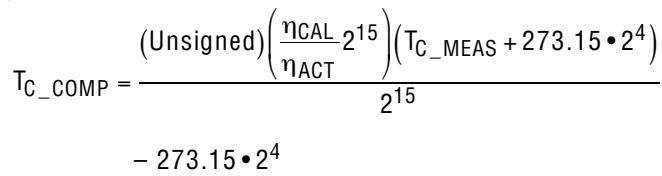
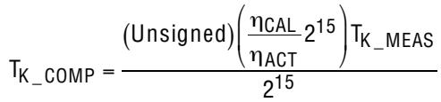
temperature error of $0 . 0 1 ^ { \circ }$ at $1 2 5 ^ { \circ } 0$ . Multiplying this 16‑bit unsigned number and the measured Kelvin (unsigned) temperature represented as a 16-bit number, yields a 32‑bit unsigned result. To scale this number back to a 13‑bit temperature (9-bit integer part, and a 4-bit fractional part), divide the number by $2 ^ { 1 5 }$ per Equation (5). Similarly, Celsius coded temperature values can be scaled using 16-bit fixed-point arithmetic, using Equation (6). In both cases, the scaled result will have a 9-bit integer (d[12:4]) and the 4LSBs (d[3:0]) representing the 4-bit fractional part. To convert the corrected result to decimal, divide the final result by $2 ^ { 4 }$ or 16, as you would the register contents. If ideality factor scaling is implemented in the target application, it is beneficial to configure the LTC2990 for Kelvin coded results to limit the number of math operations required in the target processor.
$$
T _ {K _ C O M P} = \frac {\left(\text {Unsigned}\right) \left(\frac {\eta_ {C A L}}{\eta_ {A C T}} 2 ^ {1 5}\right) T _ {K _ M E A S}}{2 ^ {1 5}}\tag{5}
$$
$$
\begin{array}{r l} T _ {C _ C O M P} & = \frac {\left(\text { Unsigned }\right) \left(\frac {\eta_ {C A L}}{\eta_ {A C T}} 2 ^ {1 5}\right) \left(T _ {C _ M E A S} + 2 7 3 . 1 5 \cdot 2 ^ {4}\right)}{2 ^ {1 5}} \ & - 2 7 3. 1 5 \cdot 2 ^ {4} \end{array}\tag{6}
$$
Sampling Currents
Single-ended voltage measurements are directly sampled by the internal ADC. The average ADC input current is a function of the input applied voltage as follows:
$$
I _ {I N (A V G)} = \left(V _ {I N} - 1. 4 9 \mathrm{V}\right) \cdot 0. 1 7 [ \mu \mathrm{A} / \mathrm{V} ]
$$
Inputs with source resistance less than 200Ω will yield full-scale gain errors due to source impedance of <1/2LSB for 14-bit conversions. The nominal conversion time is 1.5ms for single-ended conversions.
Current Measurements
The LTC2990 has the ability to perform 14-bit current measurements with the addition of a current sense resistor (see Figure 3).
In order to achieve accurate current sensing a few details must be considered. Differential voltage or current measurements are directly sampled by the internal ADC.
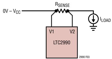
Figure 3. Simplified Current Sense Schematic
The average ADC input current for each leg of the differential input signal during a conversion is $( \mathsf { V } _ { | \mathsf { N } } - 1 . 4 9 \mathsf { V } )$ $\bullet 0 . 3 4 [ \mu \sf N ]$ . The maximum source impedance to yield 14-bit results with, 1/2LSB full-scale error is ~50Ω. In order to achieve high accuracy 4-point, or Kelvin connected measurements of the sense resistor differential voltage are necessary.
In the case of current measurements, the external sense resistor is typically small, and determined by the fullscale input voltage of the LTC2990. The full-scale differential voltage is 0.300V. The external sense resistance is then a function of the maximum measurable current, or $\mathsf { R } _ { \mathsf { E X T _ M A X } } = 0 . 3 0 0 \mathsf { V / / \mu _ { M A X } }$ . For example, if you wanted to measure a current range of ±5A, the external shunt resistance would equal 0.300V/5A = 60mΩ.
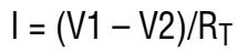
There exists a way to improve the sense resistor’s precision using the LTC2990. The LTC2990 measures both differential voltage and remote temperature. It is therefore, possible to compensate for the absolute resistance tolerance of the sense resistor and the temperature coefficient of the sense resistor in software. The resistance would be measured by running a calibrated test current through the discrete resistor. The LTC2990 would measure both the differential voltage across this resistor and the resistor temperature. From this measurement, $\mathtt { R } _ { 0 }$ and TO in the equation below would be known. Using the two equations, the host microprocessor could compensate for both the absolute tolerance and the TCR.
$$
R _ {T} = R _ {0} \bullet [ 1 + \alpha (T - T _ {0}) ]
$$
where:
$$
\alpha = + 3 9 3 0 \mathrm{ppm} / ^ {\circ} \mathrm{C} \text { for copper trace }
$$
$$
\alpha = \pm 2 \text { to } \sim + 2 0 0 \mathrm{ppm/} ^ {\circ} \mathrm{C} \text { for discrete R }\tag{7}
$$
$$
I = (V 1 - V 2) / R _ {T}\tag{8}
$$
APPLICATIONS INFORMATION
Device Configuration
The LTC2990 is configured by writing the control register through the serial interface. Refer to Table 5 for control register bit definition. The device is capable of many application configurations including voltage, temperature and current measurements. It is possible to configure the device for single or repeated acquisitions. The device can make single measurements, or in continuous mode, repeated acquisitions. When the device is configured for multiple measurements, the order of the measurements is fixed. For repeated acquisitions, only an initial trigger is required after which data registers are continuously refreshed with new data. As each new data result is ready, the MSB of the corresponding data register is set, and the corresponding status register bit is set. These bits are cleared when the corresponding data register is addressed. The configuration register value at power-up causes the part to measure only the internal temperature sensor when triggered. The four input pins V1 through V4 will be in a high impedance state, until configured otherwise, and a measurement is triggered. The data registers are double-buffered in order to ensure upper and lower data bytes do not become out of sync. Read operations must be terminated in order to avoid an indefinitely paused wait state. Reading the STATUS register does not interrupt measurement data updates. In a polling system, it is recommended that the STATUS register be tested for new data, this prevents unnecessary delays updating the measurement registers.
Data Format
The data registers are broken into 8-bit upper and lower bytes. Voltage and current conversions are 14-bits. The upper bits in the MSB registers provide status on the resulting conversions. These status bits are different for temperature and voltage conversions:
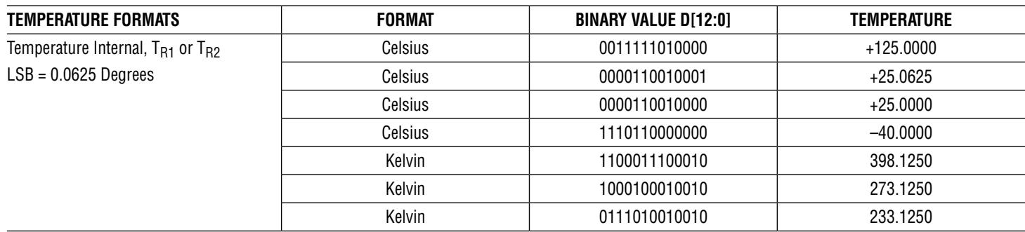
Temperature: Temperature conversions are reported as Celsius or Kelvin results described in Table 8 and Table 9, each with 0.0625 degree-weighted LSBs. The format is controlled by the control register, Bit 7. All temperature formats, TINT, TR1 and TR2 are controlled by this bit. The Temperature MSB result register most significant bit (Bit 7) is the DATA_VALID bit, which indicates whether the current register contents have been accessed since the result was written to the register. This bit will be set when new data is written to the register, and cleared when accessed. Bit 6 of the register is a sensor-shorted alarm. This bit of the corresponding register will be high if the remote sensor diode differential voltage is below 0.14V. The LTC2990 internal bias circuitry maintains this voltage above this level during normal operating conditions. Bit 5 of the register is a sensor open alarm. This bit of the corresponding register will be high if the remote sensor diode differential voltage is above $1 . 0 \mathsf { V } _ { \mathsf { D C } }$ . The LTC2990 internal bias circuitry maintains this voltage below this level during normal operating conditions. The two sensor alarms are only valid after a completed conversion indicated by the data_valid bit being high. Bit 4 through Bit 0 of the MSB register are the conversion result bits D[12:8], in two’s compliment format. Note in Kelvin results, the result will always be positive. The LSB register contains temperature result bits D[7:0]. To convert the register contents to temperature, use the following equation:
T = D[12:0]/16.
See Table 10 for conversion value examples.
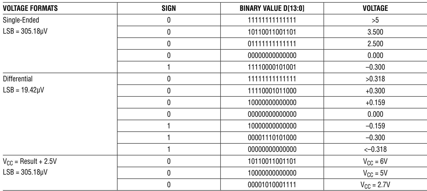
Voltage/Current: Voltage results are reported in two respective registers, an MSB and LSB register. The Voltage MSB result register most significant bit (Bit 7) is the data_valid bit, which indicates whether the current register contents have been accessed since the result was written to the register. This bit will be set when the register contents are new, and cleared when accessed. Bit 6 of the MSB register is the sign bit, Bits 5 though 0 represent bits D[13:8] of the two’s complement conversion result. The LSB register holds conversion bits D[7:0]. The LSB value is different for single-ended voltage measurements V1 through V4, and differential (current measurements) V1 – V2 and V3 – V4. Single-ended voltages are limited to positive values in the range 0V to 3.5V. Differential voltages can have input values in the range of –0.300V to 0.300V.
Use the following equations to convert the register values (see Table 10 for examples):
VSINGLE-ENDED = D[14:0] • 305.18µV, if Sign = 0
VSINGLE-ENDED = (D[14:0] +1) • –305.18µV, if Sign = 1
VDIFFERENTIAL = D[14:0] • 19.42µV, if Sign = 0
VDIFFERENTIAL = (D[14:0] +1) • –19.42µV, if Sign = 1
APPLICATIONS INFORMATION
Current = D[14:0] • 19.42µV/RSENSE, if Sign = 0 $\mathsf { C u r r e n t } = ( \overline { { \mathsf { D } [ 1 4 : 0 ] } } + 1 ) \bullet - 1 9 . 4 2 \mu \mathsf { V } / \mathsf { P } _ { \mathsf { S E N S E } } , \mathsf { i f } \mathsf { S i g n } = 1$ where RSENSE is the current sensing resistor, typically <1Ω.
VCC: The LTC2990 measures $\mathsf { V } _ { \mathsf { C } } { \mathsf { C } }$ . To convert the contents of the $\mathsf { V } _ { \mathsf { C } \mathsf { C } }$ register to voltage, use the following equation:
$$
V _ {C C} = 2. 5 + D [ 1 3: 0 ] \cdot 3 0 5. 1 8 \mu V
$$
Digital Interface
The LTC2990 communicates with a bus master using a two-wire interface compatible with the $| ^ { 2 } 0$ Bus and the SMBus, an $| ^ { 2 } 0$ extension for low power devices.
The LTC2990 is a read-write slave device and supports SMBus bus Read Byte Data and Write Byte Data, Read Word Data and Write Word Data commands. The data formats for these commands are shown in Table 3 throughTable 10.
The connected devices can only pull the bus wires LOW and can never drive the bus HIGH. The bus wires are externally connected to a positive supply voltage via a current source or pull-up resistor. When the bus is free, both lines are HIGH. Data on the $| ^ { 2 } 0$ bus can be transferred at rates of up to 100kbit/s in the standard mode and up to 400kbit/s in the fast mode. Each device on the $| ^ { 2 } 0$ bus is recognized by a unique address stored in that device and can operate as either a transmitter or receiver, depending on the function of the device. In addition to transmitters and receivers, devices can also be considered as masters or slaves when performing data transfers. A master is the device which initiates a data transfer on the bus and generates the clock signals to permit that transfer. At the same time any device addressed is considered a slave.
The LTC2990 can only be addressed as a slave. Once addressed, it can receive configuration bits or transmit the last conversion result. Therefore the serial clock line SCL is an input only and the data line SDA is bidirectional. The device supports the standard mode and the fast mode for data transfer speeds up to 400kbit/s. The Timing Diagram shows the definition of timing for fast/ standard mode devices on the $| ^ { 2 } 0$ bus. The internal state machine cannot update internal data registers during an $I ^ { 2 } C$ read operation. The state machine pauses until the $\iota ^ { 2 } C$ read is complete. It is therefore, important not to leave the LTC2990 in this state for long durations, or increased conversion latency will be experienced.
START and STOP Conditions
When the bus is idle, both SCL and SDA must be high. A bus master signals the beginning of a transmission with a START condition by transitioning SDA from high to low while SCL is high. When the bus is in use, it stays busy if a repeated START (SR) is generated instead of a STOP condition. The repeated START (SR) conditions are functionally identical to the START (S). When the master has finished communicating with the slave, it issues a STOP condition by transitioning SDA from low to high while SCL is high. The bus is then free for another transmission.
I2C Device Addressing
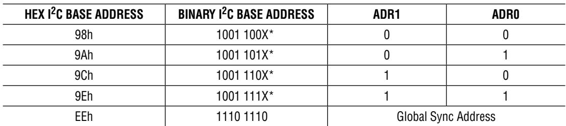
Four distinct bus addresses are configurable using the ADR0-ADR1 pins. There is also one global sync address available at EEh which provides an easy way to synchronize multiple LTC2990s on the same $| ^ { 2 } \bar { \mathsf { C } }$ bus. This allows write only access to all 2990s on the bus for simultaneous triggering. Table 2 shows the correspondence between ADR0 and ADR1 pin states and addresses.
Acknowledge
The acknowledge signal is used for handshaking between the transmitter and the receiver to indicate that the last byte of data was received. The transmitter always releases the SDA line during the acknowledge clock pulse. When the slave is the receiver, it must pull down the SDA line so that it remains LOW during this pulse to acknowledge receipt of the data. If the slave fails to acknowledge by leaving SDA HIGH, then the master can abort the transmission by generating a STOP condition. When the master is receiving data from the slave, the master must pull down the SDA line during the clock pulse to indicate receipt of the data. After the last byte has been received the master will leave the SDA line HIGH (not acknowledge) and issue a STOP condition to terminate the transmission.
Write Protocol
The master begins communication with a START condition followed by the seven bit slave address and the R/W#
APPLICATIONS INFORMATION
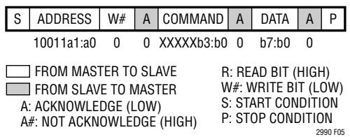
bit set to zero. The addressed LTC2990 acknowledges the address and then the master sends a command byte which indicates which internal register the master wishes to write. The LTC2990 acknowledges the command byte and then latches the lower four bits of the command byte into its internal Register Address pointer. The master then delivers the data byte and the LTC2990 acknowledges once more and latches the data into its internal register. The transmission is ended when the master sends a STOP condition. If the master continues sending a second data byte, as in a Write Word command, the second data byte will be acknowledged by the LTC2990 and written to the next register in sequence, if this register has write access.
Read Protocol
The master begins a read operation with a START condition followed by the seven bit slave address and the R/W# bit set to zero. The addressed LTC2990 acknowledges this and then the master sends a command byte which indicates which internal register the master wishes to read. The LTC2990 acknowledges this and then latches the lower four bits of the command byte into its internal Register Address pointer. The master then sends a repeated START condition followed by the same seven bit address with the R/W# bit now set to one. The LTC2990 acknowledges and sends the contents of the requested register. The transmission is ended when the master sends a STOP condition. The register pointer is automatically incremented after each byte is read. If the master acknowledges the transmitted data byte, as in a Read Word command, the LTC2990 will send the contents of the next sequential register as the second data byte. The byte following register 0x0F is register 0x00, or the status register.
Control Register
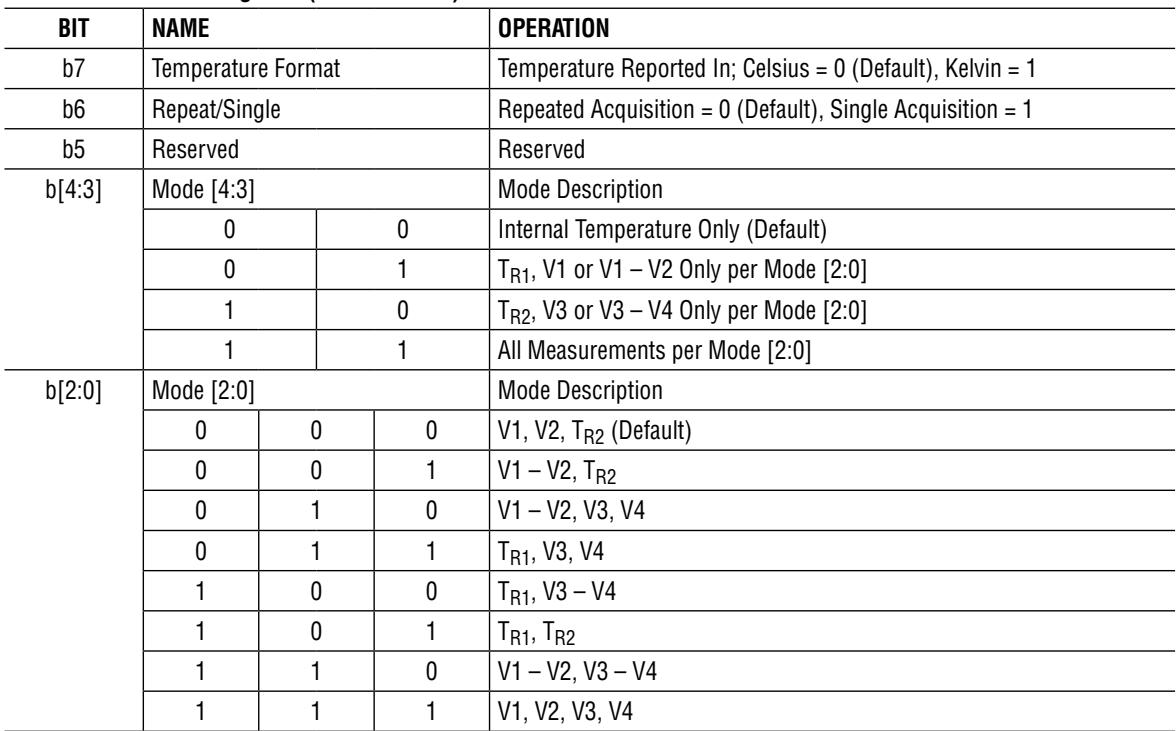
The control register (Table 5) determines the selected measurement mode of the device. The LTC2990 can be configured to measure voltages, currents and temperatures. These measurements can be single-shot or repeated measurements. Temperatures can be set to report in Celsius or Kelvin temperature scales. The LTC2990 can be configured to run particular measurements, or all possible measurements per the configuration specified by the mode bits. The power-on default configuration of the control register is set to 0x00, which translates to a repeated measurement of the internal temperature sensor, when triggered. This mode prevents the application of remote diode test currents on pins V1 and V3, and remote diode terminations on pins V2 and V4 at power-up.
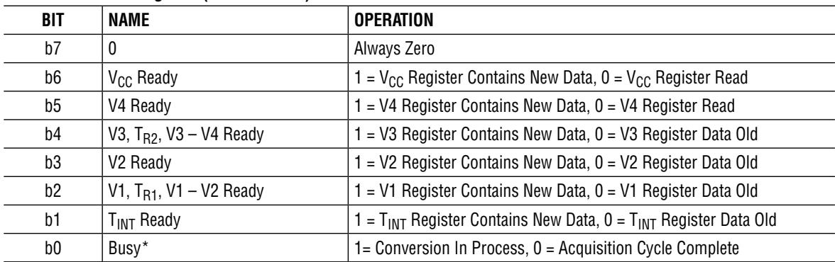
Status Register
The status register (Table 4) reports the status of a particular conversion result. When new data is written into a particular result register, the corresponding DATA_VALID bit is set. When the register is addressed by the I2C interface, the status bit (as well as the DATA_VALID bit in the respective register) is cleared. The host can then determine if the current available register data is new or stale. The busy bit, when high, indicates a single-shot conversion is in progress. The busy bit is always high during repeated mode, after the initial conversion is triggered.

Figure 4. Data Transfer Over I2C or SMBus
| S | ADDRESS | W# | A | COMMAND | A | DATA | A | P |
| 10011a1:a0 | 0 | 0 | XXXXb3:b0 | 0 | b7:b0 | 0 | ||
| □ | FROM MASTER TO SLAVE | R: READ BIT (HIGH) | ||||||
| ■ | FROM SLAVE TO MASTER | W#: WRITE BIT (LOW) | ||||||
| A: ACKNOWLEDGE (LOW) | S: START CONDITION | |||||||
| A#: NOT ACKNOWLEDGE (HIGH) | P: STOP CONDITION | |||||||
Figure 5. LTC2990 Serial Bus Write Byte Protoco
APPLICATIONS INFORMATION
| S | ADDRESS | W# | A | COMMAND | A | DATA | A | DATA | A | P |
| 10011a1:a0 | 0 | 0 | XXXXb3:b0 | 0 | b7:b0 | 0 | b7:b0 | 0 |
Figure 6. LTC2990 Serial Bus Repeated Write Byte Protocol
| S | ADDRESS | W# | A | COMMAND | A | S | ADDRESS | R | A | DATA | A# | P |
| 10011a1:a0 | 0 | 0 | XXXXXb3:b0 | 0 | 10011a1:a0 | 1 | 0 | b7:b0 | 1 |
Figure 7. LTC2990 Serial Bus Read Byte Protocol
| S | ADDRESS | W# | A | COMMAND | A | S | ADDRESS | R | A | DATA | A | DATA | A# | P |
| 10011a1:a0 | 0 | 0 | XXXXXb3:b0 | 0 | 10011a1:a0 | 1 | 0 | b7:b0 | 0 | b7:b0 | 1 |
Figure 8. LTC2990 Serial Bus Repeated Read Byte Protocol
Table 2. I2C Base Address
| HEX I2C BASE ADDRESS | BINARY I2C BASE ADDRESS | ADR1 | ADRO |
| 98h | 1001 100X* | 0 | 0 |
| 9Ah | 1001 101X* | 0 | 1 |
| 9Ch | 1001 110X* | 1 | 0 |
| 9Eh | 1001 111X* | 1 | 1 |
| EEh | 1110 1110 | Global Sync Address | |
*X = R/W Bit
Table 3. LTC2990 Register Address and Contents
| REGISTER ADDRESS*† | REGISTER NAME | READ/WRITE | DESCRIPTION |
| 00h | STATUS | R | Indicates BUSY State, Conversion Status |
| 01h | CONTROL | R/W | Controls Mode, Single/Repeat, Celsius/Kelvin |
| 02h | TRIGGER** | R/W | Triggers an Conversion |
| 03h | N/A | Unused Address | |
| 04h | $T_{INT}$ (MSB) | R | Internal Temperature MSB |
| 05h | $T_{INT}$ (LSB) | R | Internal Temperature LSB |
| 06h | V1 (MSB) | R | V1, V1 – V2 or $T_{R1}$ MSB |
| 07h | V1 (LSB) | R | V1, V1 – V2 or $T_{R1}$ LSB |
| 08h | V2 (MSB) | R | V2, V1 – V2 or $T_{R1}$ MSB |
| 09h | V2 (LSB) | R | V2, V1 – V2 or $T_{R1}$ LSB |
| 0Ah | V3 (MSB) | R | V3, V3 – V4 or $T_{R2}$ MSB |
| 0Bh | V3 (LSB) | R | V3, V3 – V4 or $T_{R2}$ LSB |
| 0Ch | V4 (MSB) | R | V4, V3 – V4 or $T_{R2}$ MSB |
| 0Dh | V4 (LSB) | R | V4, V3 – V4 or $T_{R2}$ LSB |
| 0Eh | $V_{CC}$ (MSB) | R | $V_{CC}$ MSB |
| 0Fh | $V_{CC}$ (LSB) | R | $V_{CC}$ LSB |
*Register Address MSBs b7-b4 are ignored.
**Writing any value triggers a conversion. Data Returned reading this register address is the Status register.
†Power-on reset sets all registers to 00h.
APPLICATIONS INFORMATION
Table 4. STATUS Register (Default 0x00)
| BIT | NAME | OPERATION |
| b7 | 0 | Always Zero |
| b6 | $V_{CC}$ Ready | 1 = $V_{CC}$ Register Contains New Data, 0 = $V_{CC}$ Register Read |
| b5 | V4 Ready | 1 = V4 Register Contains New Data, 0 = V4 Register Read |
| b4 | V3, $T_{R2}$ , V3 – V4 Ready | 1 = V3 Register Contains New Data, 0 = V3 Register Data Old |
| b3 | V2 Ready | 1 = V2 Register Contains New Data, 0 = V2 Register Data Old |
| b2 | V1, $T_{R1}$ , V1 – V2 Ready | 1 = V1 Register Contains New Data, 0 = V1 Register Data Old |
| b1 | $T_{INT}$ Ready | 1 = $T_{INT}$ Register Contains New Data, 0 = $T_{INT}$ Register Data Old |
| b0 | Busy* | 1= Conversion In Process, 0 = Acquisition Cycle Complete |
*In Repeat mode, Busy = 1 always
Table 5. CONTROL Register (Default 0x00)
| BIT | NAME | OPERATION | ||
| b7 | Temperature Format | Temperature Reported In; Celsius = 0 (Default), Kelvin = 1 | ||
| b6 | Repeat/Single | Repeated Acquisition = 0 (Default), Single Acquisition = 1 | ||
| b5 | Reserved | Reserved | ||
| b[4:3] | Mode [4:3] | Mode Description | ||
| 0 | 0 | Internal Temperature Only (Default) | ||
| 0 | 1 | $T_{R1}$ , V1 or V1 – V2 Only per Mode [2:0] | ||
| 1 | 0 | $T_{R2}$ , V3 or V3 – V4 Only per Mode [2:0] | ||
| 1 | 1 | All Measurements per Mode [2:0] | ||
| b[2:0] | Mode [2:0] | Mode Description | ||
| 0 | 0 | 0 | V1, V2, $T_{R2}$ (Default) | |
| 0 | 0 | 1 | V1 – V2, $T_{R2}$ | |
| 0 | 1 | 0 | V1 – V2, V3, V4 | |
| 0 | 1 | 1 | $T_{R1}$ , V3, V4 | |
| 1 | 0 | 0 | $T_{R1}$ , V3 – V4 | |
| 1 | 0 | 1 | $T_{R1}$ , $T_{R2}$ | |
| 1 | 1 | 0 | V1 – V2, V3 – V4 | |
| 1 | 1 | 1 | V1, V2, V3, V4 | |
APPLICATIONS INFORMATION
Table 6. Voltage/Current Measurement MSB Data Register Format
| BIT 7 | BIT 6 | BIT 5 | BIT 4 | BIT 3 | BIT 2 | BIT 1 | BIT 0 |
| DV* | Sign | D13 | D12 | D11 | D10 | D9 | D8 |
*Data Valid is set when a new result is written into the register. Data Valid is cleared when this register is addressed (read) by the I2C interface.
Table 7. Voltage/Current Measurement LSB Data Register Format
| BIT 7 | BIT 6 | BIT 5 | BIT 4 | BIT 3 | BIT 2 | BIT 1 | BIT 0 |
| D7 | D6 | D5 | D4 | D3 | D2 | D1 | D0 |
Table 8. Temperature Measurement MSB Data Register Format
| BIT 7 | BIT 6 | BIT 5 | BIT 4 | BIT 3 | BIT 2 | BIT 1 | BIT 0 |
| DV* | SS** | S0† | D12 | D11 | D10 | D9 | D8 |
*DATA_VALID is set when a new result is written into the register. DATA_VALID is cleared when this register is addressed (read) by the I2C interface.
**Sensor Short is high if the voltage measured on V1 is too low during temperature measurements. This signal is always low for TINT measurements.
†Sensor Open is high if the voltage measured on V1 is excessive during temperature measurements. This signal is always low for TINT measurements.
| BIT 7 | BIT 6 | BIT 5 | BIT 4 | BIT 3 | BIT 2 | BIT 1 | BIT 0 |
| D7 | D6 | D5 | D4 | D3 | D2 | D1 | D0 |
Table 9. Temperature Measurement LSB Data Register Format
APPLICATIONS INFORMATION
Table 10. Conversion Formats
| VOLTAGE FORMATS | SIGN | BINARY VALUE D[13:0] | VOLTAGE |
| Single-EndedLSB = 305.18μV | 0 | 11111111111111 | >5 |
| 0 | 10110011001101 | 3.500 | |
| 0 | 011111111111111 | 2.500 | |
| 0 | 00000000000000 | 0.000 | |
| 1 | 11110000101001 | -0.300 | |
| DifferentialLSB = 19.42μV | 0 | 11111111111111 | >0.318 |
| 0 | 11110001011000 | +0.300 | |
| 0 | 10000000000000 | +0.159 | |
| 0 | 00000000000000 | 0.000 | |
| 1 | 10000000000000 | -0.159 | |
| 1 | 00001110101000 | -0.300 | |
| 1 | 00000000000000 | <-0.318 | |
| $V_{CC}$ =Result + 2.5VLSB = 305.18μV | 0 | 10110011001101 | $V_{CC}$ =6V |
| 0 | 10000000000000 | $V_{CC}$ =5V | |
| 0 | 00001010001111 | $V_{CC}$ =2.7V |
| TEMPERATURE FORMATS | FORMAT | BINARY VALUE D[12:0] | TEMPERATURE |
| Temperature Internal, $T_{R1}$ or $T_{R2}$ LSB = 0.0625 Degrees | Celsius | 001111010000 | +125.0000 |
| Celsius | 0000110010001 | +25.0625 | |
| Celsius | 0000110010000 | +25.0000 | |
| Celsius | 1110110000000 | -40.0000 | |
| Kelvin | 1100011100010 | 398.1250 | |
| Kelvin | 1000100010010 | 273.1250 | |
| Kelvin | 0111010010010 | 233.1250 |
TYPICAL APPLICATIONS
VOLTAGE, CURRENT AND TEMPERATURE CONFIGURATION:CONTROL REGISTER: 0x58
High Voltage/Current and Temperature Monitoring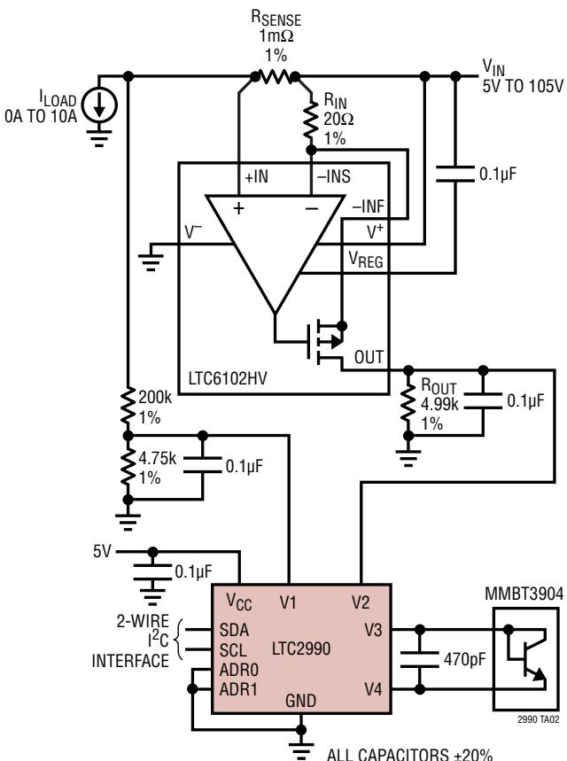
TAMB REG 4, 5 0.0625°C/LSB VLOAD REG 6, 7 13.2mVLSB V2(ILOAD) REG 8, 9 1.223mA/LSB TREMOTE REG A, B 0.0625°C/LSB VCC REG E, F 2.5V + 305.18µV/LSB
Computer Voltage and Temperature Monitoring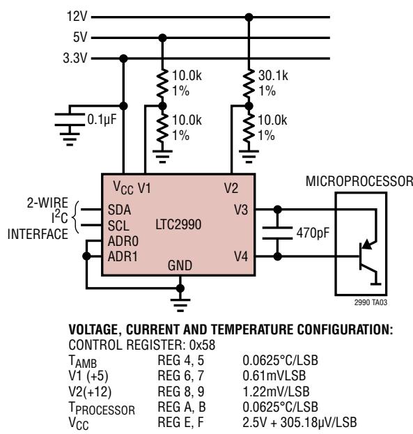
TYPICAL APPLICATIONS
Motor Protection/Regulation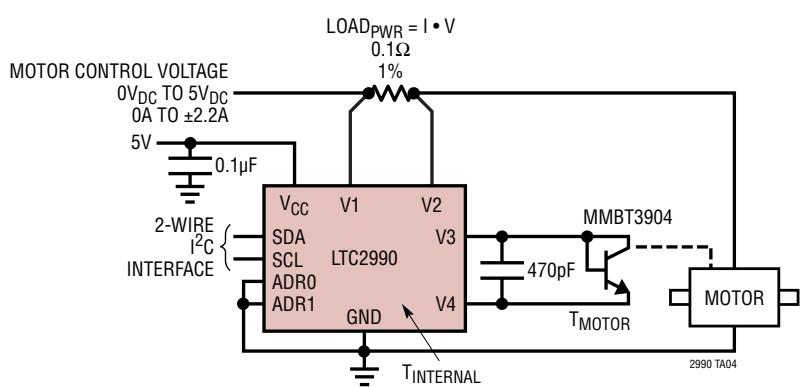
| CURRENT AND TEMPERATURE CONFIGURATION: | VOLTAGE AND TEMPERATURE CONFIGURATION: | ||||
| CONTROL REGISTER: 0x59 | CONTROL REGISTER: 0x58 | ||||
| $T_{AMB}$ | REG 4, 5 | 0.0625°C/LSB | $T_{AMB}$ | REG 4, 5 | 0.0625°C/LSB |
| $I_{MOTOR}$ | REG 6, 7 | 194μA/LSB | $V_{MOTOR}$ | REG 8, 9 | 305.18μVLSB |
| $T_{MOTOR}$ | REG A, B | 0.0625°C/LSB | $T_{MOTOR}$ | REG A, B | 0.0625°C/LSB |
| $V_{CC}$ | REG E, F | 2.5V + 305.18μV/LSB | $V_{CC}$ | REG E, F | 2.5V + 305.18μV/LSB |
Large Motor Protection/Regulation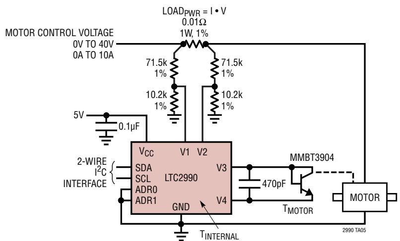
| VOLTAGE AND TEMPERATURE CONFIGURATION: | CURRENT AND TEMPERATURE CONFIGURATION: | ||||
| CONTROL REGISTER: 0x58 | CONTROL REGISTER: 0x59 | ||||
| $T_{AMB}$ | REG 4, 5 | 0.0625°C/LSB | $T_{AMB}$ | REG 4, 5 | 0.0625°C/LSB |
| $V_{MOTOR}$ | REG 8, 9 | 2.44mVLSB | $I_{MOTOR}$ | REG 6, 7 | 15.54mA/LSB |
| $T_{MOTOR}$ | REG A, B | 0.0625°C/LSB | $T_{MOTOR}$ | REG A, B | 0.0625°C/LSB |
| $V_{CC}$ | REG E, F | 2.5V + 305.18μV/LSB | $V_{CC}$ | REG E, F | 2.5V + 305.18μV/LSB |
TYPICAL APPLICATIONS
Fan/Air Filter/Temperature Alarm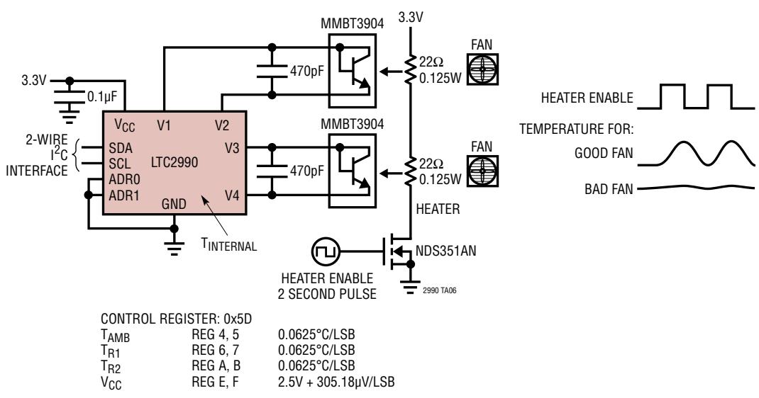
Battery Monitoring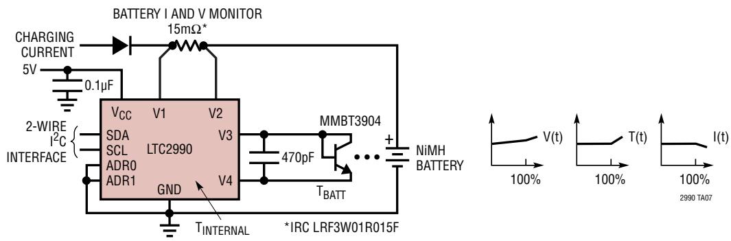
| VOLTAGE AND TEMPERATURE CONFIGURATION: | CURRENT AND TEMPERATURE CONFIGURATION: | ||||
| CONTROL REGISTER: 0x58 | CONTROL REGISTER: 0x59 | ||||
| $T_{AMB}$ | REG 4, 5 | 0.0625°C/LSB | $T_{AMB}$ | REG 4, 5 | 0.0625°C/LSB |
| $V_{BAT}$ | REG 8, 9 | 305.18μVLSB | $I_{BAT}$ | REG 6, 7 | 1.295mA/LSB |
| $T_{BAT}$ | REG A, B | 0.0625°C/LSB | $T_{BAT}$ | REG A, B | 0.0625°C/LSB |
| $V_{CC}$ | REG E, F | 2.5V + 305.18μV/LSB | $V_{CC}$ | REG E, F | 2.5V + 305.18μV/LSB |
TYPICAL APPLICATIONS
Wet-Bulb Psychrometer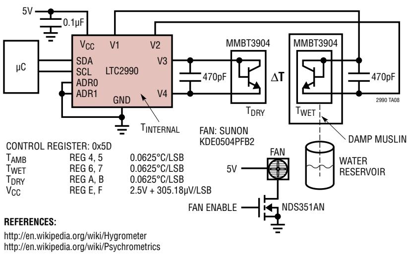
http://en.wikipedia.org/wiki/Hygrometer http://en.wikipedia.org/wiki/Psychrometrics
Wind Direction/Instrumentation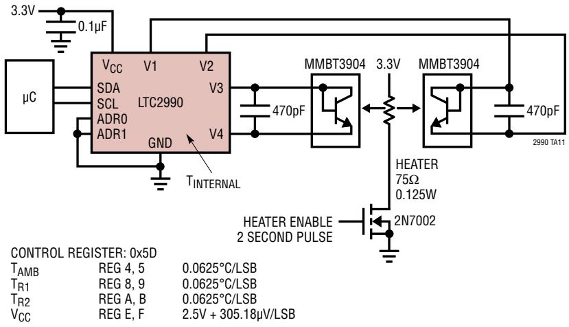
TYPICAL APPLICATIONS
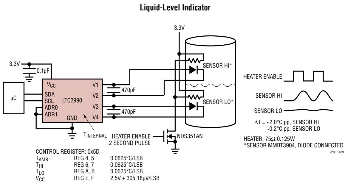
Oscillator/Reference Oven Temperature Regulation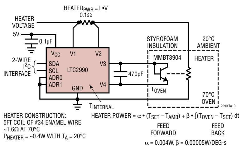
| VOLTAGE AND TEMPERATURE CONFIGURATION: | CURRENT AND TEMPERATURE CONFIGURATION: | ||||
| CONTROL REGISTER: 0x58 | CONTROL REGISTER: 0x59 | ||||
| $T_{AMB}$ | REG 4, 5 | 0.0625°C/LSB | $T_{AMB}$ | REG 4, 5 | 0.0625°C/LSB |
| V1, V2 | REG 8, 9 | 305.18μVLSB | $I_{HEATER}$ | REG 6, 7 | 269μVLSB |
| $T_{OVEN}$ | REG A, B | 0.0625°C/LSB | $T_{HEATER}$ | REG A, B | 0.0625°C/LSB |
| $V_{CC}$ | REG E, F | 2.5V + 305.18μV/LSB | $V_{CC}$ | REG E, F | 2.5V + 305.18μV/LSB |
PACKAGE DESCRIPTION
MS Package 10-Lead Plastic MSOP (Reference LTC DWG # 05-08-1661 Rev F)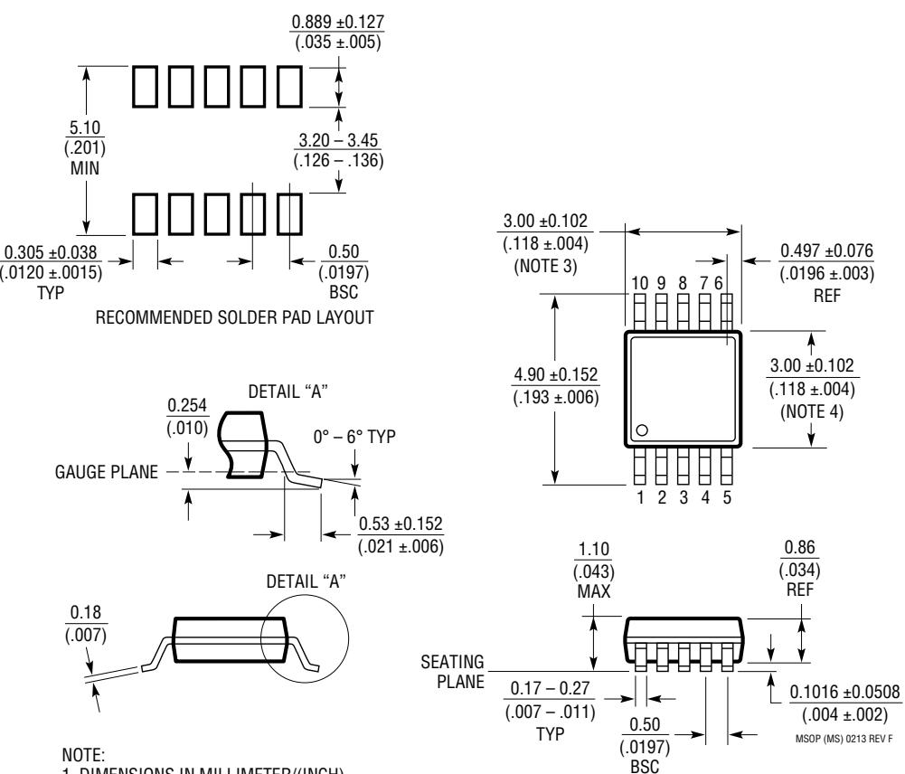
NOTE:
DIMENSIONS IN MILLIMETER/(INCH)
DRAWING NOT TO SCALE
DIMENSION DOES NOT INCLUDE MOLD FLASH, PROTRUSIONS OR GATE BURRS.
MOLD FLASH, PROTRUSIONS OR GATE BURRS SHALL NOT EXCEED 0.152mm (.006") PER SIDEDIMENSION DOES NOT INCLUDE INTERLEAD FLASH OR PROTRUSIONS.
INTERLEAD FLASH OR PROTRUSIONS SHALL NOT EXCEED 0.152mm (.006") PER SIDE
- LEAD COPLANARITY (BOTTOM OF LEADS AFTER FORMING) SHALL BE 0.102mm (.004") MAX
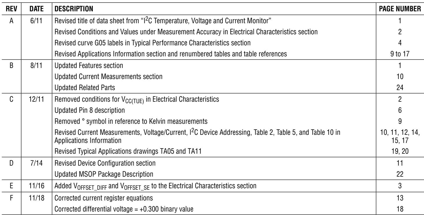
REVISION HISTORY
| REV | DATE | DESCRIPTION | PAGE NUMBER |
| A | 6/11 | Revised title of data sheet from “ $I^{2}C$ Temperature, Voltage and Current Monitor” | 1 |
| Revised Conditions and Values under Measurement Accuracy in Electrical Characteristics section | 2 | ||
| Revised curve G05 labels in Typical Performance Characteristics section | 4 | ||
| Revised Applications Information section and renumbered tables and table references | 9 to 17 | ||
| B | 8/11 | Updated Features section | 1 |
| Updated Current Measurements section | 10 | ||
| Updated Related Parts | 24 | ||
| C | 12/11 | Removed conditions for $V_{CC(TUE)}$ in Electrical Characteristics | 2 |
| Updated Pin 8 description | 6 | ||
| Removed ° symbol in reference to Kelvin measurements | 9 | ||
| Revised Current Measurements, Voltage/Current, $I^{2}C$ Device Addressing, Table 2, Table 5, and Table 10 in Applications Information | 10, 11, 12, 14, 15, 17 | ||
| Revised Typical Applications drawings TA05 and TA11 | 19, 20 | ||
| D | 7/14 | Revised Device Configuration section | 11 |
| Updated MSOP Package Description | 22 | ||
| E | 11/16 | Added $V_{OFFSET\_DIFF}$ and $V_{OFFSET\_SE}$ to the Electrical Characteristics section | 3 |
| F | 11/18 | Corrected current register equations | 13 |
| Corrected differential voltage = +0.300 binary value | 18 |
TYPICAL APPLICATION
High Voltage/Current and Temperature Monitoring
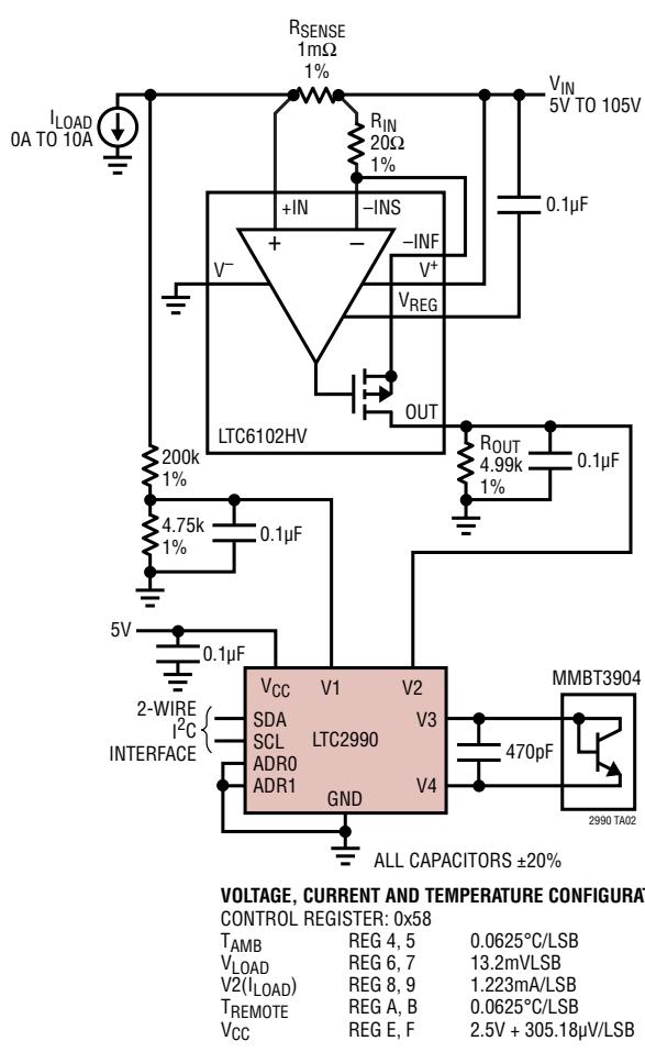
TREMOTE TREMOTE REG A, B 0.0625°C/LSB
VCC REG E, F 2.5V + 305.18µV/LSB
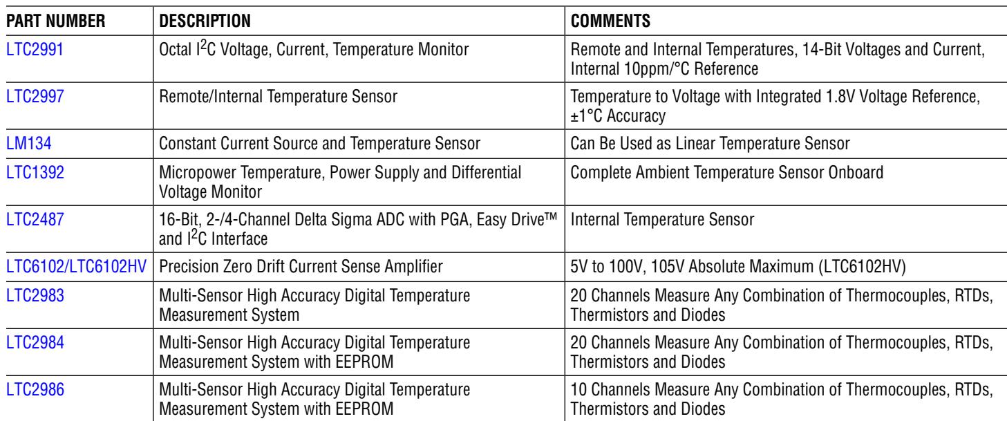
RELATED PARTS
| PART NUMBER | DESCRIPTION | COMMENTS |
| LTC2991 | Octal I2C Voltage, Current, Temperature Monitor | Remote and Internal Temperatures, 14-Bit Voltages and Current, Internal 10ppm/°C Reference |
| LTC2997 | Remote/Internal Temperature Sensor | Temperature to Voltage with Integrated 1.8V Voltage Reference, ±1°C Accuracy |
| LM134 | Constant Current Source and Temperature Sensor | Can Be Used as Linear Temperature Sensor |
| LTC1392 | Micropower Temperature, Power Supply and Differential Voltage Monitor | Complete Ambient Temperature Sensor Onboard |
| LTC2487 | 16-Bit, 2-/4-Channel Delta Sigma ADC with PGA, Easy DriveTM and I2C Interface | Internal Temperature Sensor |
| LTC6102/LTC6102HV | Precision Zero Drift Current Sense Amplifier | 5V to 100V, 105V Absolute Maximum (LTC6102HV) |
| LTC2983 | Multi-Sensor High Accuracy Digital Temperature Measurement System | 20 Channels Measure Any Combination of Thermocouples, RTDs, Thermistors and Diodes |
| LTC2984 | Multi-Sensor High Accuracy Digital Temperature Measurement System with EEPROM | 20 Channels Measure Any Combination of Thermocouples, RTDs, Thermistors and Diodes |
| LTC2986 | Multi-Sensor High Accuracy Digital Temperature Measurement System with EEPROM | 10 Channels Measure Any Combination of Thermocouples, RTDs, Thermistors and Diodes |
Figures and diagrams from the PDF
Preview the extracted datasheet assets and open any image in a separate tab for closer inspection.


















Use this datasheet from any agent
Send the page, markdown, chunks, or search endpoint to ChatGPT, Claude, embedr-app, or your own tooling.