
ADS7039
Small-Size, Low-Power, 10-Bit, 2-MSPS, SAR ADC
ADS7039-Q1 Small-Size, Low-Power, 10-Bit, 2-MSPS, SAR ADC
1 Features
1• Qualified for Automotive Applications
• AEC-Q100 Qualified With the Following Results:
Device Temperature Grade $1 : - 4 0 ^ { \circ } \mathsf { C }$ to $1 2 5 ^ { \circ } \mathrm { C }$ Ambient Operating Temperature Range
– Device HBM ESD Classification Level ±2000 V
– Device CDM ESD Classification Level ±1000 V
• Ultra-Low Power Consumption:
– 1.2 mW (max) at 2 MSPS with 3-V AVDD
– Less Than 1 µW at 1 kSPS with 3-V AVDD
• Miniature Footprint:
– 8-Pin VSSOP Package: 2.30 mm × 2.00 mm
• 2-MSPS Throughput with Zero Data Latency
• Wide Operating Range:
– AVDD: 2.35 V to 3.6 V
– DVDD: 1.65 V to 3.6 V (Independent of AVDD)
– Temperature Range: $\scriptscriptstyle - 4 0 ^ { \circ } \mathsf { C }$ to $+ 1 2 5 ^ { \circ } \mathrm { C }$
• Excellent Performance:
– 10-Bit Resolution with NMC
– ±0.4 LSB DNL; ±0.4 LSB INL
– 61-dB SNR with 3-V AVDD
– –75-dB THD with 3-V AVDD
• Unipolar Input Range: 0 V to AVDD
• Integrated Offset Calibration
• SPI-Compatible Serial Interface: 32 MHz
• JESD8-7A Compliant Digital I/O
2 Applications
• Automotive Infotainment
• Automotive Sensors
• Level Sensors
• Ultrasonic Flow Meters
• Motor Control
• Portable Medical Equipment
3 Description
The ADS7039-Q1 device is a an automotive Q100- qualified, 10-bit, 2-MSPS, analog-to-digital converter (ADC). The device supports a wide analog input voltage range (2.35 V to 3.6 V) and includes a capacitor-based, successive-approximation register (SAR) ADC with an inherent sample-and-hold circuit. The SPI-compatible serial interface is controlled by the CS and SCLK signals. The input signal is sampled with the CS falling edge and SCLK is used for conversion and serial data output. The device supports a wide digital supply range (1.65 V to 3.6 V), enabling direct interface to a variety of host controllers. The ADS7039-Q1 complies with the JESD8-7A standard for a normal DVDD range (1.65 V to 1.95 V).
The ADS7039-Q1 is available in an 8-pin, miniature, VSSOP package and is specified for operation from –40°C to +125°C. The fast sampling rate of the ADS7039-Q1, along with miniature form-factor and low-power consumption, makes this device suitable for space-constrained and fast-scanning automotive applications.
Device Information(1)
| PART NAME | PACKAGE | BODY SIZE (NOM) |
| ADS7039-Q1 | VSSOP (8) | 2.30 mm × 2.00 mm |
(1) For all available packages, see the orderable addendum at the end of the datasheet.
Typical Application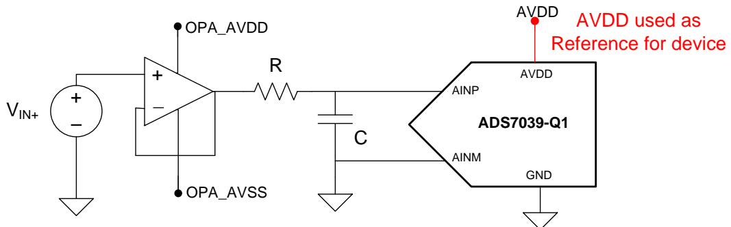
Copyright © 2016, Texas Instruments Incorporated
Table of Contents
1 Features.... 1
2 Applications.... 1
3 Description.... 1
4 Revision History.... 2
5 Pin Configuration and Functions.... 3
6 Specifications.... 4
6.1 Absolute Maximum Ratings.... 4
6.2 ESD Ratings.... 4
6.3 Recommended Operating Conditions.... 4
6.4 Thermal Information.... 4
6.5 Electrical Characteristics.... 5
6.6 Timing Requirements.... 6
6.7 Switching Characteristics.... 6
6.8 Typical Characteristics.... 7
7 Parameter Measurement Information.... 12
7.1 Digital Voltage Levels.... 12
8 Detailed Description.... 12
8.1 Overview.... 12
8.2 Functional Block Diagram.... 13
8.3 Feature Description.... 13
8.4 Device Functional Modes.... 17
9 Application and Implementation.... 20
9.1 Application Information.... 20
9.2 Typical Application.... 20
10 Power Supply Recommendations.... 23
10.1 AVDD and DVDD Supply Recommendations.... 23
10.2 Estimating Digital Power Consumption.... 23
10.3 Optimizing Power Consumed by the Device.... 23
11 Layout.... 24
11.1 Layout Guidelines.... 24
11.2 Layout Example.... 24
12 Device and Documentation Support.... 25
12.1 Documentation Support.... 25
12.2 Receiving Notification of Documentation Updates.... 25
12.3 Community Resources.... 25
12.4 Trademarks.... 25
12.5 Electrostatic Discharge Caution.... 25
12.6 Glossary.... 25
13 Mechanical, Packaging, and Orderable Information.... 25
4 Revision History
NOTE: Page numbers for previous revisions may differ from page numbers in the current version.
Changes from Original (January 2017) to Revision A Page
- Changed Timing Diagram figure to correct SCLK and SDO traces....6
- Changed number of conversion bits from 12 to 10 and number of SCLKs from 14 to 12 in first paragraph of Serial Interface section....16
5 Pin Configuration and Functions

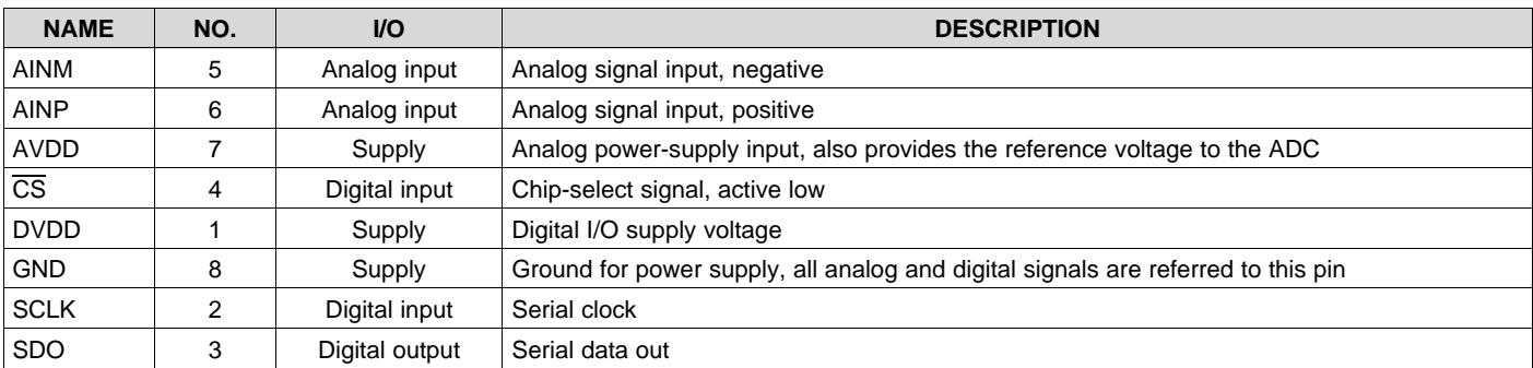
Pin Functions
| NAME | NO. | I/O | DESCRIPTION |
| AINM | 5 | Analog input | Analog signal input, negative |
| AINP | 6 | Analog input | Analog signal input, positive |
| AVDD | 7 | Supply | Analog power-supply input, also provides the reference voltage to the ADC |
| $\overline{CS}$ | 4 | Digital input | Chip-select signal, active low |
| DVDD | 1 | Supply | Digital I/O supply voltage |
| GND | 8 | Supply | Ground for power supply, all analog and digital signals are referred to this pin |
| SCLK | 2 | Digital input | Serial clock |
| SDO | 3 | Digital output | Serial data out |
6 Specifications
6.1 Absolute Maximum Ratings(1)
| MIN | MAX | UNIT | |
| AVDD to GND | -0.3 | 3.9 | V |
| DVDD to GND | -0.3 | 3.9 | V |
| AINP to GND | -0.3 | AVDD + 0.3 | V |
| AINM to GND | -0.3 | 0.3 | V |
| Digital input voltage to GND | -0.3 | DVDD + 0.3 | V |
| Storage temperature, $T_{stg}$ | -60 | 150 | °C |
(1) Stresses beyond those listed under Absolute Maximum Ratings may cause permanent damage to the device. These are stress ratings only, which do not imply functional operation of the device at these or any other conditions beyond those indicated under Recommended Operating Conditions. Exposure to absolute-maximum-rated conditions for extended periods may affect device reliability.
6.2 ESD Ratings
| VALUE | UNIT | ||
| $V_{(ESD)}$ Electrostatic discharge | Human-body model (HBM), per AEC Q100-002 $^{(1)}$ | ±2000 | V |
| Charged-device model (CDM), per AEC Q100-011 | ±1000 | ||
(1) AEC Q100-002 indicates that HBM stressing shall be in accordance with the ANSI/ESDA/JEDEC JS-001 specification.
6.3 Recommended Operating Conditions
over operating free-air temperature range (unless otherwise noted)
| MIN | NOM | MAX | UNIT | ||
| AVDD | Analog supply voltage range | 2.35 | 3.6 | V | |
| DVDD | Digital supply voltage range | 1.65 | 3.6 | V | |
| $T_A$ | Operating free-air temperature | -40 | 125 | °C | |
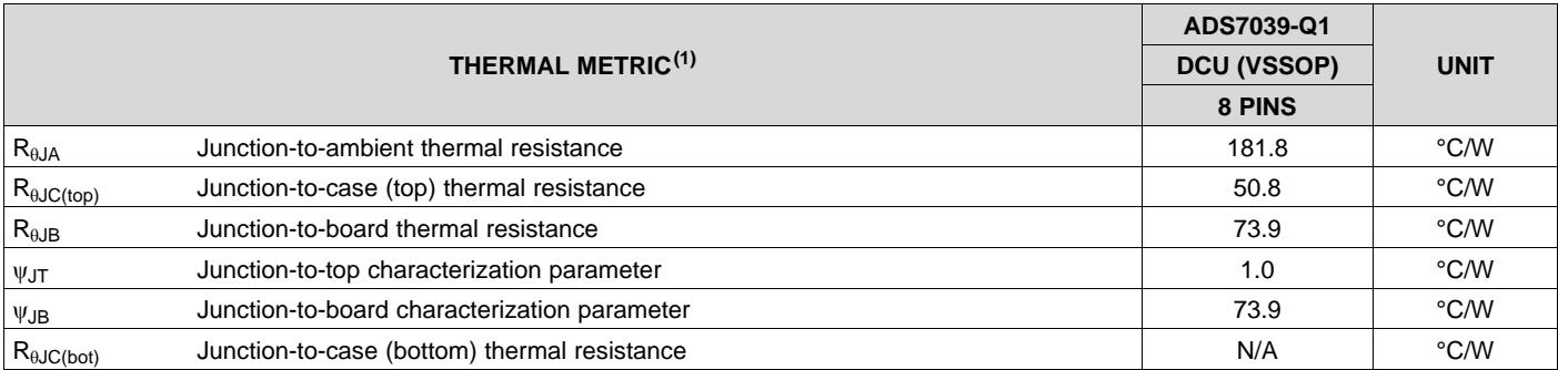
6.4 Thermal Information
| THERMAL METRIC(1) | ADS7039-Q1 | UNIT | |
| DCU (VSSOP) | |||
| 8 PINS | |||
| $R_{\theta JA}$ | Junction-to-ambient thermal resistance | 181.8 | °C/W |
| $R_{\theta JC(top)}$ | Junction-to-case (top) thermal resistance | 50.8 | °C/W |
| $R_{\theta JB}$ | Junction-to-board thermal resistance | 73.9 | °C/W |
| $\psi_{JT}$ | Junction-to-top characterization parameter | 1.0 | °C/W |
| $\psi_{JB}$ | Junction-to-board characterization parameter | 73.9 | °C/W |
| $R_{\theta JC(bot)}$ | Junction-to-case (bottom) thermal resistance | N/A | °C/W |
(1) For more information about traditional and new thermal metrics, see the Semiconductor and IC Package Thermal Metrics application report.
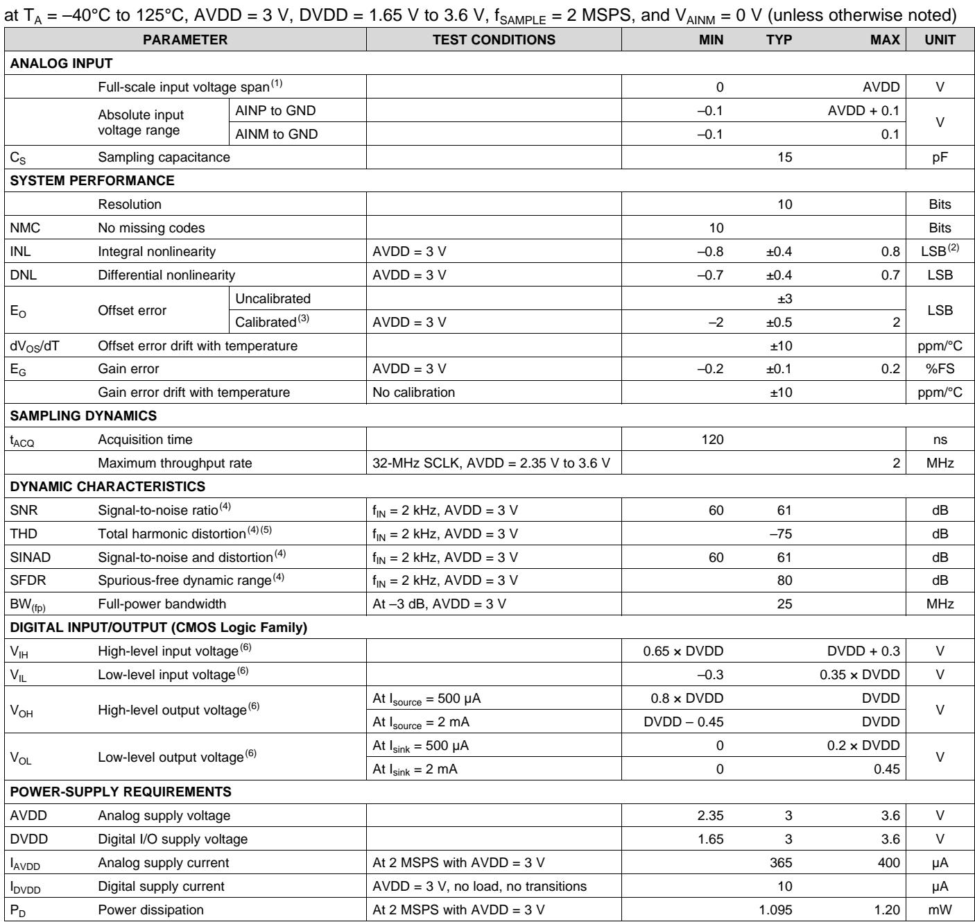
6.5 Electrical Characteristics
| PARAMETER | TEST CONDITIONS | MIN | TYP | MAX | UNIT | |
| ANALOG INPUT | ||||||
| Full-scale input voltage span(1) | 0 | AVDD | V | |||
| Absolute input voltage range | AINP to GND | -0.1 | AVDD + 0.1 | V | ||
| AINM to GND | -0.1 | 0.1 | ||||
| CSSampling capacitance | 15 | pF | ||||
| SYSTEM PERFORMANCE | ||||||
| Resolution | 10 | Bits | ||||
| NMC No missing codes | 10 | Bits | ||||
| INL Integral nonlinearity | AVDD = 3 V | -0.8 | ±0.4 | 0.8 | LSB(2) | |
| DNL Differential nonlinearity | AVDD = 3 V | -0.7 | ±0.4 | 0.7 | LSB | |
| EO Offset error | Uncalibrated | ±3 | LSB | |||
| Calibrated(3) | AVDD = 3 V | -2 | ±0.5 | 2 | ||
| dVOS/dT Offset error drift with temperature | ±10 | ppm/°C | ||||
| EG Gain error | AVDD = 3 V | -0.2 | ±0.1 | 0.2 | %FS | |
| Gain error drift with temperature | No calibration | ±10 | ppm/°C | |||
| SAMPLING DYNAMICS | ||||||
| tACQ Acquisition time | 120 | ns | ||||
| Maximum throughput rate | 32-MHz SCLK, AVDD = 2.35 V to 3.6 V | 2 | MHz | |||
| DYNAMIC CHARACTERISTICS | ||||||
| SNR Signal-to-noise ratio(4) | fIN= 2 kHz, AVDD = 3 V | 60 | 61 | dB | ||
| THD Total harmonic distortion(4)(5) | fIN= 2 kHz, AVDD = 3 V | -75 | dB | |||
| SINAD Signal-to-noise and distortion(4) | fIN= 2 kHz, AVDD = 3 V | 60 | 61 | dB | ||
| SFDR Spurious-free dynamic range(4) | fIN= 2 kHz, AVDD = 3 V | 80 | dB | |||
| BW(fp) Full-power bandwidth | At -3 dB, AVDD = 3 V | 25 | MHz | |||
| DIGITAL INPUT/OUTPUT (CMOS Logic Family) | ||||||
| VIH High-level input voltage(6) | 0.65 × DVDD | DVDD + 0.3 | V | |||
| VIL Low-level input voltage(6) | -0.3 | 0.35 × DVDD | V | |||
| VOH High-level output voltage(6) | At Isource= 500 μA | 0.8 × DVDD | DVDD | V | ||
| At Isource= 2 mA | DVDD - 0.45 | DVDD | ||||
| VOL Low-level output voltage(6) | At Isink= 500 μA | 0 | 0.2 × DVDD | V | ||
| At Isink= 2 mA | 0 | 0.45 | ||||
| POWER-SUPPLY REQUIREMENTS | ||||||
| AVDD Analog supply voltage | 2.35 | 3 | 3.6 | V | ||
| DVDD Digital I/O supply voltage | 1.65 | 3 | 3.6 | V | ||
| IAVDD Analog supply current | At 2 MSPS with AVDD = 3 V | 365 | 400 | μA | ||
| IDVDD Digital supply current | AVDD = 3 V, no load, no transitions | 10 | μA | |||
| PD Power dissipation | At 2 MSPS with AVDD = 3 V | 1.095 | 1.20 | mW | ||
(1) Ideal input span; does not include gain or offset error.
(2) LSB means least significant bit.
(3) See the Offset Calibration section for more details.
(4) All specifications expressed in decibels (dB) refer to the full-scale input (FSR) and are tested with an input signal 0.5 dB below full-scale, unless otherwise specified.
(5) Calculated on the first nine harmonics of the input frequency.
(6) Digital voltage levels comply with the JESD8-7A standard for DVDD from 1.65 V to 1.95 V; see the Digital Voltage Levels section for more details.
6.6 Timing Requirements
all specifications are at $\mathsf { T } _ { \mathsf { A } } = - 4 0 ^ { \circ } \mathsf { C }$ to 125°C, AVDD = 2.35 V to 3.6 V, DVDD = 1.65 V to 3.6 V, and $\mathsf { C } _ { \mathsf { L O A D } }$ on SDO = 20 pF (unless otherwise specified)
| MIN | TYP | MAX | UNIT | ||
| $t_{ACQ}$ | Acquisition time | 120 | ns | ||
| $f_{SCLK}$ | SCLK frequency | 0.016 | 28 | MHz | |
| $t_{SCLK}$ | SCLK period | 35.7 | ns | ||
| $t_{PH\_CK}$ | SCLK high time | 0.45 | 0.55 | $t_{SCLK}$ | |
| $t_{PL\_CK}$ | SCLK low time | 0.45 | 0.55 | $t_{SCLK}$ | |
| $t_{PH\_CS}$ | $\overline{CS}$ high time | 30 | ns | ||
| $t_{SU\_CSCK}$ | Setup time: $\overline{CS}$ falling to SCLK falling | 12 | ns | ||
| $t_{D\_CKCS}$ | Delay time: last SCLK falling to $\overline{CS}$ rising | 10 | ns | ||
6.7 Switching Characteristics
all specifications are at $\mathsf { T } _ { \mathsf { A } } = - 4 0 ^ { \circ } \mathsf { C }$ to 125°C, AVDD = 2.35 V to 3.6 V, DVDD = 1.65 V to 3.6 V, and $\mathsf { C } _ { \mathsf { L O A D } }$ on SDO = 20 pF (unless otherwise specified)
| PARAMETER | TEST CONDITIONS | MIN | TYP | MAX | UNIT | |
| $f_{THROUGHPUT}$ | Throughput | 2 | MSPS | |||
| $t_{CYCLE}$ | Cycle time | 0.5 | μs | |||
| $t_{CONV}$ | Conversion time | 10.5 × $t_{SCLK} + t_{SU\_CSCK}$ | ns | |||
| $t_{DV\_CSDO}$ | Delay time: $\overline{CS}$ falling to data enable | 10 | ns | |||
| $t_{D\_CKDO}$ | Delay time: SCLK falling to (next) data valid on DOUT | AVDD = 2.35 V to 3.6 V | 25 | ns | ||
| $t_{DZ\_CSDO}$ | Delay time: $\overline{CS}$ rising to DOUT going to tri-state | 5 | ns | |||
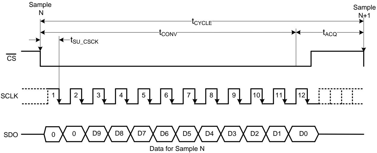
Figure 1. Timing Diagram
6.8 Typical Characteristics
at ${ \sf T } _ { \sf A } = 2 5 ^ { \circ } { \sf C }$ , AVDD = 3 V, $\mathsf { D V D D } = 1 . 8 \mathsf { V } ,$ and $\mathsf { f } _ { \mathsf { S A M P L E } } = 2$ MSPS (unless otherwise noted)

SNR = 61.39 dB, THD = –80.82 dB, f = 2 kHz, AVDD = 3 V
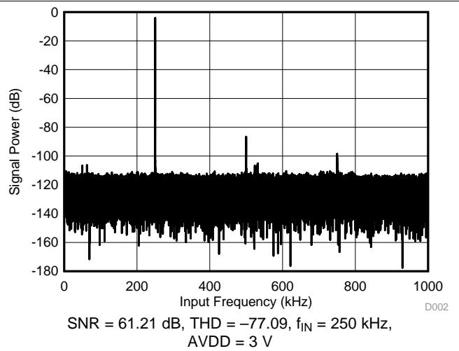
Figure 2. Typical FFT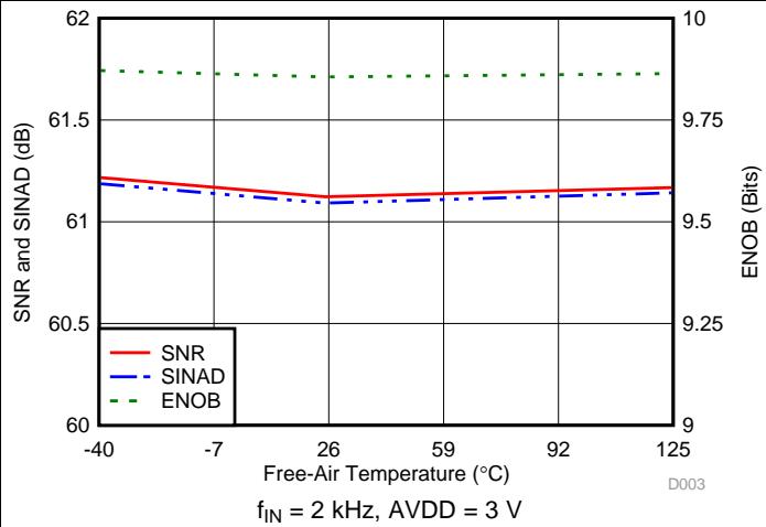
Figure 3. Typical FFT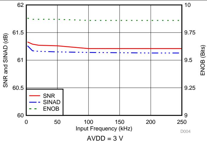
Figure 4. SNR and SINAD vs Temperature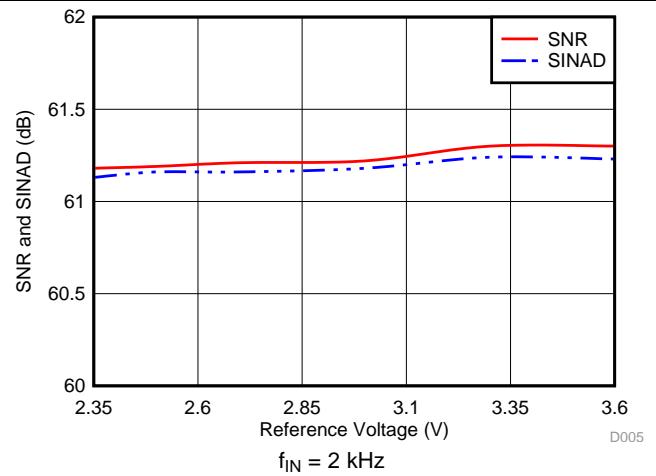
Figure 6. SNR and SINAD vs Reference Voltage (AVDD)
Figure 5. SNR and SINAD vs Input Frequency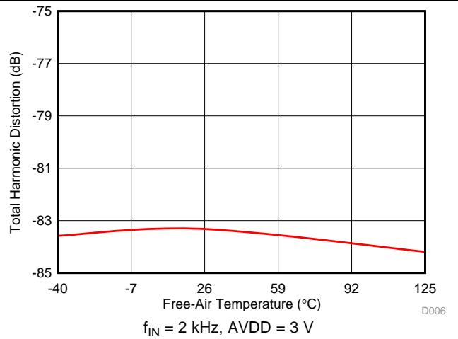
Figure 7. THD vs Temperature
Typical Characteristics (continued)
at ${ \sf T } _ { \sf A } = 2 5 ^ { \circ } { \sf C }$ , AVDD = 3 V, DVDD = 1.8 V, and $\mathbf { f } _ { \mathsf { S A M P L E } } = 2$ MSPS (unless otherwise noted)
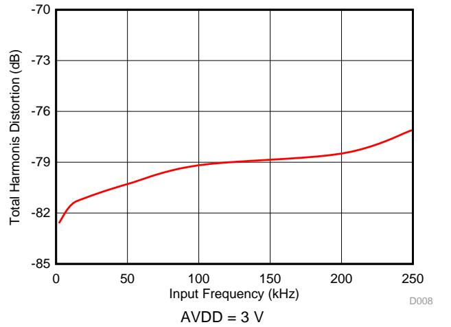
Figure 8. SFDR vs Temperature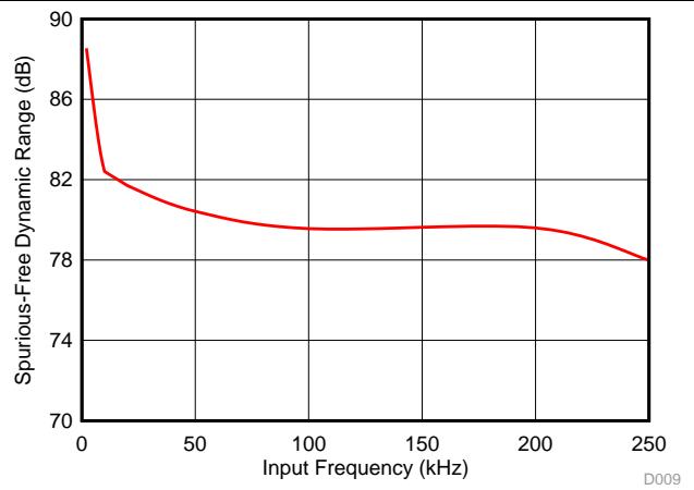
Figure 9. THD vs Input Frequency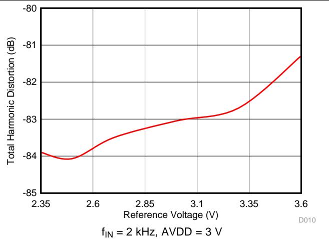
Figure 10. SFDR vs Input Frequency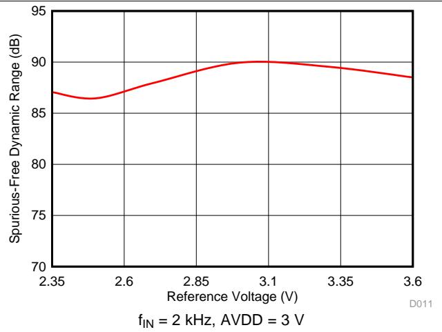
Figure 12. SFDR vs Reference Voltage (AVDD)
Figure 11. THD vs Reference Voltage (AVDD)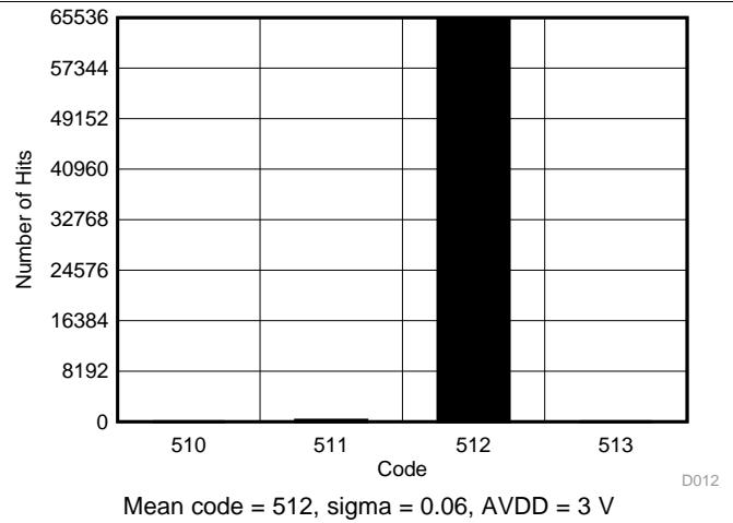
Figure 13. DC Input Histogram
Typical Characteristics (continued)
at $\bar { \mathsf { T } } _ { \mathsf { A } } = 2 5 ^ { \circ } \mathsf { C }$ , AVDD = 3 V, DVDD = 1.8 V, and $\mathbf { f } _ { \mathsf { S A M P L E } } = 2$ MSPS (unless otherwise noted)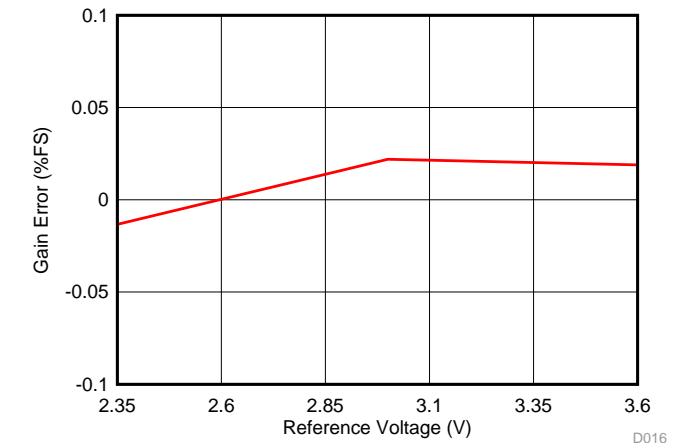
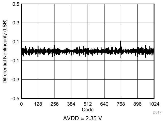
Figure 14. Gain Error vs Reference Voltage (AVDD)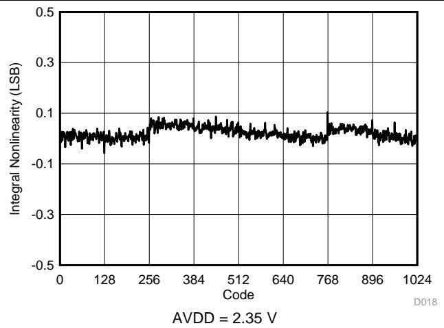
Figure 15. Typical DNL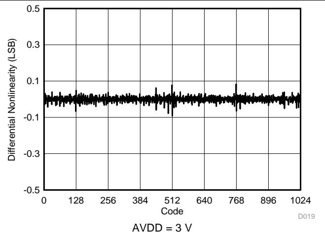
Figure 16. Typical INL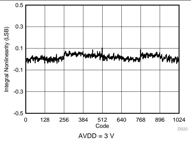
Figure 18. Typical INL
Figure 17. Typical DNL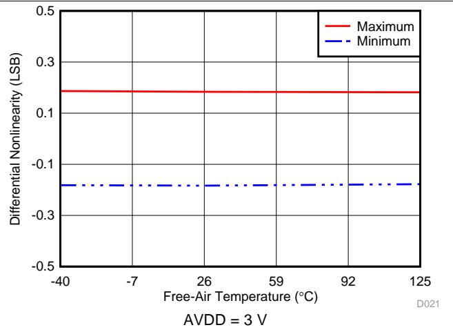
Figure 19. DNL vs Temperature
Typical Characteristics (continued)
at ${ \sf T } _ { \sf A } = 2 5 ^ { \circ } { \sf C }$ , AVDD = 3 V, DVDD = 1.8 V, and $\mathsf { f } _ { \mathsf { S A M P L E } } = 2$ MSPS (unless otherwise noted)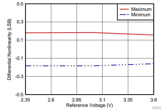

Figure 20. DNL vs Reference Voltage (AVDD)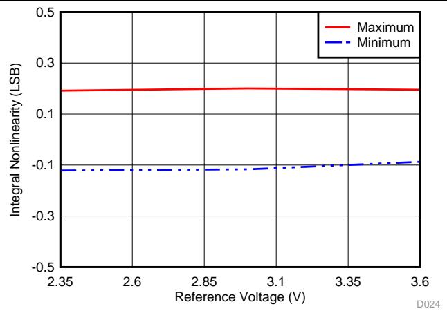
Figure 21. INL vs Temperature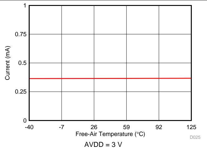
Figure 22. INL vs Reference Voltage (AVDD)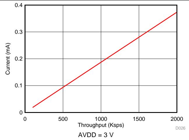
Figure 24. AVDD Supply Current vs Throughput
Figure 23. AVDD Supply Current vs Temperature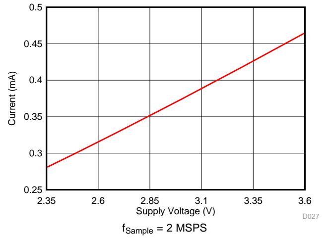
Figure 25. AVDD Supply Current vs Supply Voltage
www.ti.com
Typical Characteristics (continued)
at T = 25°C, AVDD = 3 V, DVDD = 1.8 V, and $\mathbf { f } _ { \mathsf { S A M P L E } } = 2$ MSPS (unless otherwise noted)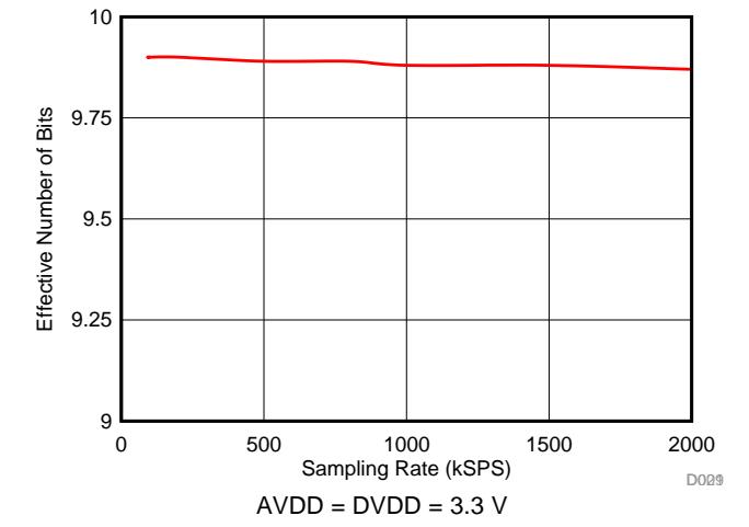

Figure 26. ENOB vs Sampling Rate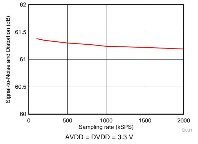
Figure 28. SINAD vs Sampling Rate
Figure 27. SNR vs Sampling Rate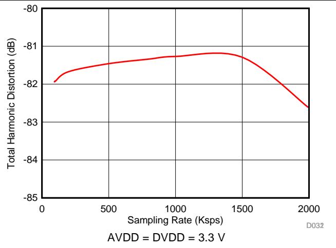
Figure 29. THD vs Sampling Rate
7 Parameter Measurement Information
7.1 Digital Voltage Levels
The device complies with the JESD8-7A standard for DVDD from 1.65 V to 1.95 V. Figure 30 shows voltage levels for the digital input and output pins.
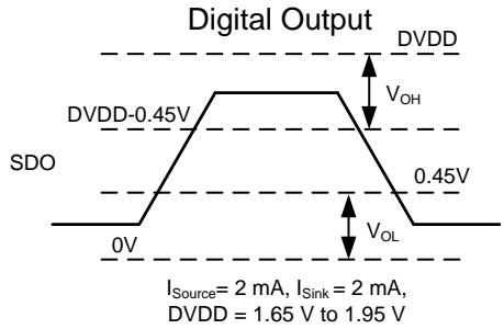

Figure 30. Digital Voltage Levels as per the JESD8-7A Standard
8 Detailed Description
8.1 Overview
The ADS7039-Q1 is an ultra-low-power, miniature analog-to-digital converter (ADC) that supports a wide analog input range. The analog input range for the device is defined by the AVDD supply voltage. The device samples the input voltage across the AINP and AINM pins on the CS falling edge and starts the conversion. The clock provided on the SCLK pin is used for conversion and data transfer. During conversions, both the AINP and AINM pins are disconnected from the sampling circuit. After the conversion completes, the sampling capacitors are reconnected across the AINP and AINM pins and the ADS7039-Q1 enters acquisition phase.
The device has an internal offset calibration. The offset calibration can be initiated by the user either on power-up or during normal operation; see the Offset Calibration section for more details.
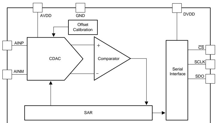
The device also provides a simple serial interface to the host controller and operates over a wide range of digital power supplies. The ADS7039-Q1 requires only a 28-MHz SCLK for supporting a throughput of 2 MSPS. The digital interface also complies with the JESD8-7A (normal range) standard. The Functional Block Diagram section provides a block diagram of the device.
8.2 Functional Block Diagram
8.3 Feature Description
8.3.1 Reference
The device uses the analog supply voltage (AVDD) as a reference, as shown in Figure 31. The AVDD pin is recommended to be decoupled with a 3.3-µF, low equivalent series resistance (ESR) ceramic capacitor.. The AVDD pin functions as a switched capacitor load to the source powering AVDD. The decoupling capacitor provides the instantaneous charge required by the internal circuit and helps in maintaining a stable dc voltage on the AVDD pin. The AVDD pin is recommended to be powered with a low output impedance and low-noise regulator (such as the TPS73230).
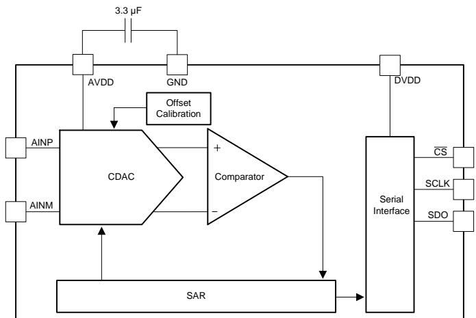
Figure 31. Reference for the Device
Feature Description (continued)
8.3.2 Analog Input
The device supports single-ended analog inputs. The ADC samples the difference between AINP and AINM and converts for this voltage. The device is capable of accepting a signal from –100 mV to 100 mV on the AINM input and is useful in systems where the sensor or signal-conditioning block is far from the ADC. In such a scenario, there can be a difference between the ground potential of the sensor or signal conditioner and the ADC ground. In such cases, use separate wires to connect the ground of the sensor or signal conditioner to the AINM pin. The AINP input is capable of accepting signals from 0 V to AVDD. Figure 32 represents the equivalent analog input circuits for the sampling stage. The device has a low-pass filter followed by the sampling switch and sampling capacitor. The sampling switch is represented by an $\mathsf { R } _ { \mathsf { S } }$ (typically 50 Ω) resistor in series with an ideal switch and ${ \sf C } _ { \sf S }$ (typically 15 pF) is the sampling capacitor. The ESD diodes are connected from both analog inputs to AVDD and ground.
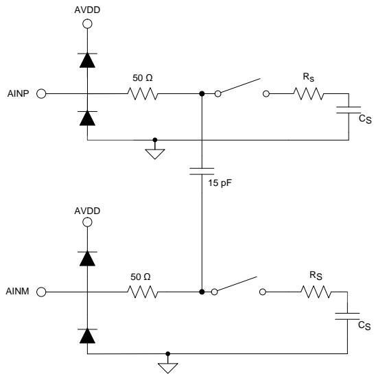
Figure 32. Equivalent Input Circuit for the Sampling Stage
The analog input full-scale range (FSR) is equal to the reference voltage of the ADC. The reference voltage for the device is equal to the analog supply voltage (AVDD). Thus, the device FSR can be determined by Equation 1:
$$
\mathrm{FSR} = \mathrm{V} _ {\mathrm{REF}} = \mathrm{AVDD}\tag{1}
$$
Feature Description (continued)
8.3.3 ADC Transfer Function
The device output is in straight binary format. The device resolution for a single-ended input can be computed by Equation 2:
$$
1 \mathrm{LSB} = V _ {\mathrm{REF}} / 2 ^ {N}
$$
where:
$\mathsf { V } _ { \mathsf { R E F } } = \mathsf { A V D D a n d }$
$\Nu = 1 0$
(2)
Figure 33 and Table 1 show the ideal transfer characteristics for the device.
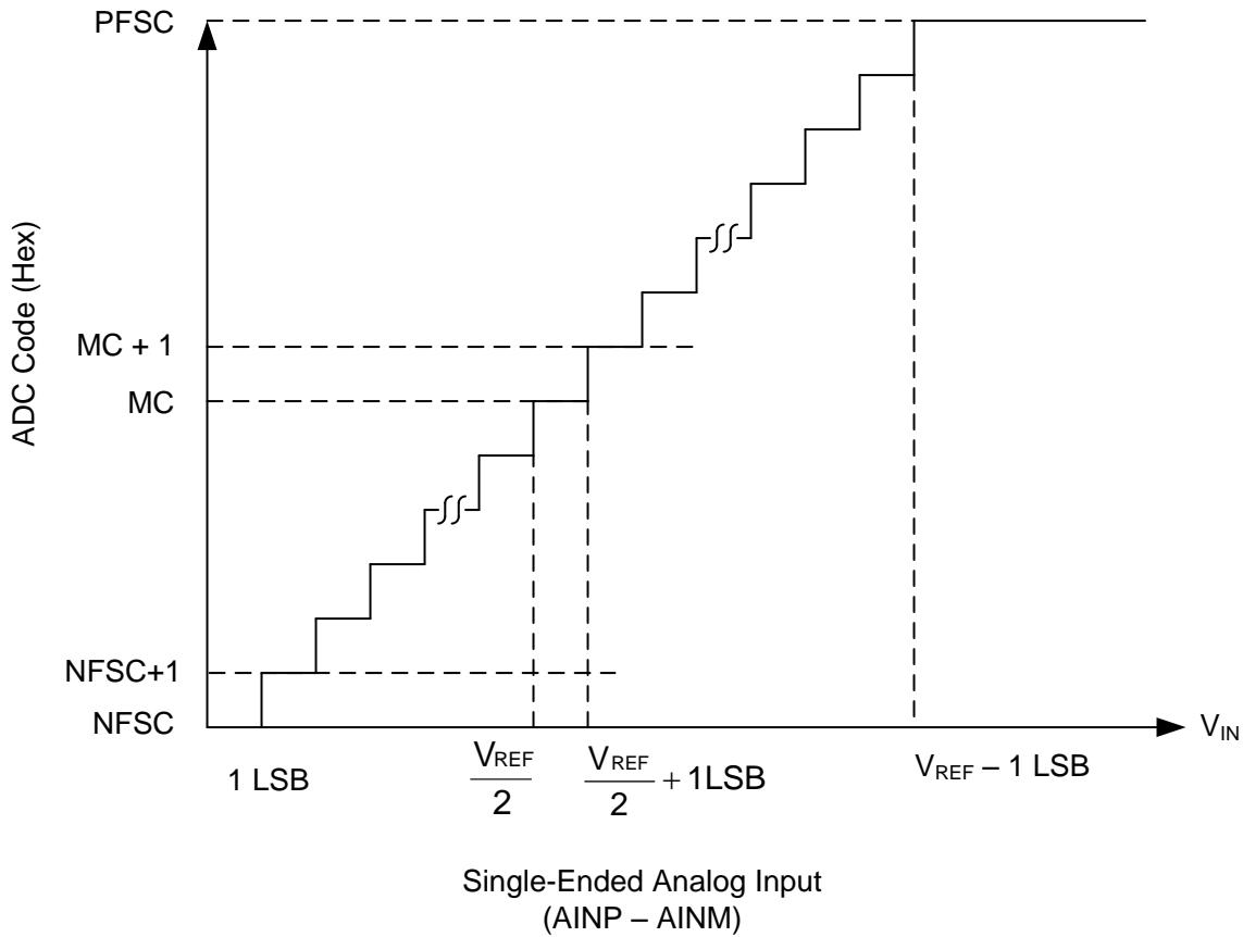
Figure 33. Ideal Transfer Characteristics
Table 1. Transfer Characteristics
| INPUT VOLTAGE (AINP – AINM) | CODE | DESCRIPTION | IDEAL OUTPUT CODE (HEX) |
| ≤1 LSB | NFSC | Negative full-scale code | 000 |
| 1 LSB to 2 LSBs | NFSC + 1 | — | 001 |
| $(V_{REF} / 2)$ to $(V_{REF} / 2) + 1$ LSB | MC | Mid code | 200 |
| $(V_{REF} / 2) + 1$ LSB to $(V_{REF} / 2) + 2$ LSBs | MC + 1 | — | 201 |
| ≥ $V_{REF} - 1$ LSB | PFSC | Positive full-scale code | 3FF |
8.3.4 Serial Interface
The device supports a simple, SPI-compatible interface to the external host. The $\overline { { \mathsf { C S } } }$ signal defines one conversion and serial transfer frame. A frame starts with a CS falling edge and ends with a CS rising edge. The SDO pin outputs the ADC conversion results. Figure 34 shows a detailed timing diagram for the serial interface. A minimum delay of $\mathfrak { t } _ { \mathtt { S U } _ { \mathtt { - } } }$ _CSCK must elapse between the CS falling edge and the first SCLK falling edge. The device uses the clock provided on the SCLK pin for conversion and data transfer. The conversion result is available on the SDO pin with the first two bits set to 0, followed by 10 bits of the conversion result. The first zero is launched on the SDO pin on the CS falling edge. Subsequent bits (starting with another 0 followed by the conversion result) are launched on the SDO pin on subsequent SCLK falling edges. The SDO output remains low after 12 SCLKs. A CS rising edge ends the frame and brings the serial data bus to tri-state. For acquisition of the next sample, a minimum time of $\mathtt { t _ { A C Q } }$ must be provided after the conversion of the current sample is completed. For details on timing specifications, see the Timing Requirements table.
The device initiates an offset calibration on the first $\overline { { \mathsf { C S } } }$ falling edge after power-up and the SDO output remains low during the first serial transfer frame after power-up. For further details, see the Offset Calibration section.

Figure 34. Serial Interface Timing Diagram
8.4 Device Functional Modes
8.4.1 Offset Calibration
The ADS7039-Q1 includes a feature to calibrate the device internal offset. During offset calibration, the analog input pins (AINP and AINM) are disconnected from the sampling stage. The device includes an internal offset calibration register (OCR) that stores the offset calibration result. The OCR is an internal register and cannot be accessed by the user through the serial interface. The OCR is reset to zero on power-up. Therefore, it is recommended to calibrate the offset on power-up in order to bring the offset error within the specified limits. If the operating temperature or analog supply voltage reflect a significant change, the offset can be recalibrated during normal operation. Figure 35 shows the offset calibration process.
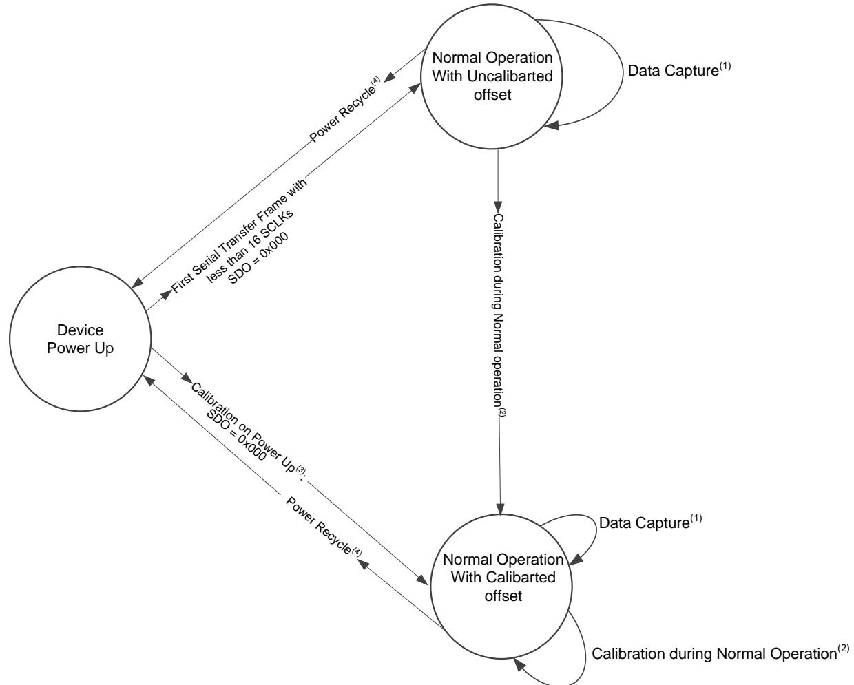
(1) See the Timing Requirements section for timing specifications.
(2) See the Offset Calibration During Normal Operation section for details.
(3) See the Offset Calibration on Power-Up section for details.
(4) The power recycle on the AVDD supply is required to reset the offset calibration and to bring the device to a power-up state.
Figure 35. Offset Calibration
Device Functional Modes (continued)
8.4.1.1 Offset Calibration on Power-Up
The device initiates offset calibration on the first CS falling edge after power-up and calibration completes if the CS pin remains low for at least 16 SCLK falling edges after the first CS falling edge. The SDO output remains low during calibration. The minimum acquisition time must be provided after calibration for acquiring the first sample. If the device is not provided with at least 16 SCLKs during the first serial transfer frame after power-up, the OCR is not updated. Table 2 provides the timing parameters for offset calibration on power-up.
For subsequent samples, the device adjusts the conversion results with the value stored in the OCR. The conversion result adjusted with the value stored in OCR is provided by the device on the SDO output. Figure 36 shows the timing diagram for offset calibration on power-up.
Table 2. Offset Calibration on Power-Up
| MIN | TYP | MAX | UNIT | ||
| $f_{CLK-CAL}$ | SCLK frequency for calibration | 14 | MHz | ||
| $t_{POWERUP-CAL}$ | Calibration time at power-up | $15 \times t_{SCLK}$ | ns | ||
| $t_{ACQ}$ | Acquisition time | 120 | ns | ||
| $t_{PH\_CS}$ | $\overline{CS}$ high time | $t_{ACQ}$ | ns | ||
| $t_{SU\_CSCK}$ | Setup time: $\overline{CS}$ falling to SCLK falling | 12 | ns | ||
| $t_{D\_CKCS}$ | Delay time: last SCLK falling to $\overline{CS}$ rising | 10 | ns | ||
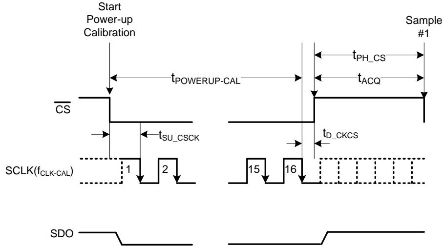
Figure 36. Offset Calibration on Power-Up Timing Diagram
8.4.1.2 Offset Calibration During Normal Operation
Offset calibration can be done during normal device operation if at least 32 SCLK falling edges are provided in one serial transfer frame. During the first 12 SCLKs, the device converts the sample acquired on the CS falling edge and provides data on the SDO output. The device initiates the offset calibration on the 17th SCLK falling edge and calibration completes on the 32nd SCLK falling edge. The SDO output remains low after the 12th SCLK falling edge and SDO goes to tri-state after CS goes high. If the device is provided with less than 32 SCLKs during a serial transfer frame, the OCR is not updated. Table 3 provides the timing parameters for offset calibration during normal operation.
For subsequent samples, the device adjusts the conversion results with the value stored in the OCR. The conversion result adjusted with the value stored in the OCR is provided by the device on the SDO output. Figure 37 shows the timing diagram for offset calibration during normal operation.
Table 3. Offset Calibration During Normal Operation
| MIN | TYP | MAX | UNIT | ||
| $f_{CLK-CAL}$ | SCLK frequency for calibration | 14 | MHz | ||
| $t_{CAL}$ | Calibration time during normal operation | $15 \times t_{SCLK}$ | ns | ||
| $t_{ACQ}$ | Acquisition time | 120 | ns | ||
| $t_{PH\_CS}$ | $\overline{CS}$ high time | $t_{ACQ}$ | ns | ||
| $t_{SU\_CSCK}$ | Setup time: $\overline{CS}$ falling to SCLK falling | 12 | ns | ||
| $t_{D\_CKCS}$ | Delay time: last SCLK falling to $\overline{CS}$ rising | 10 | ns | ||
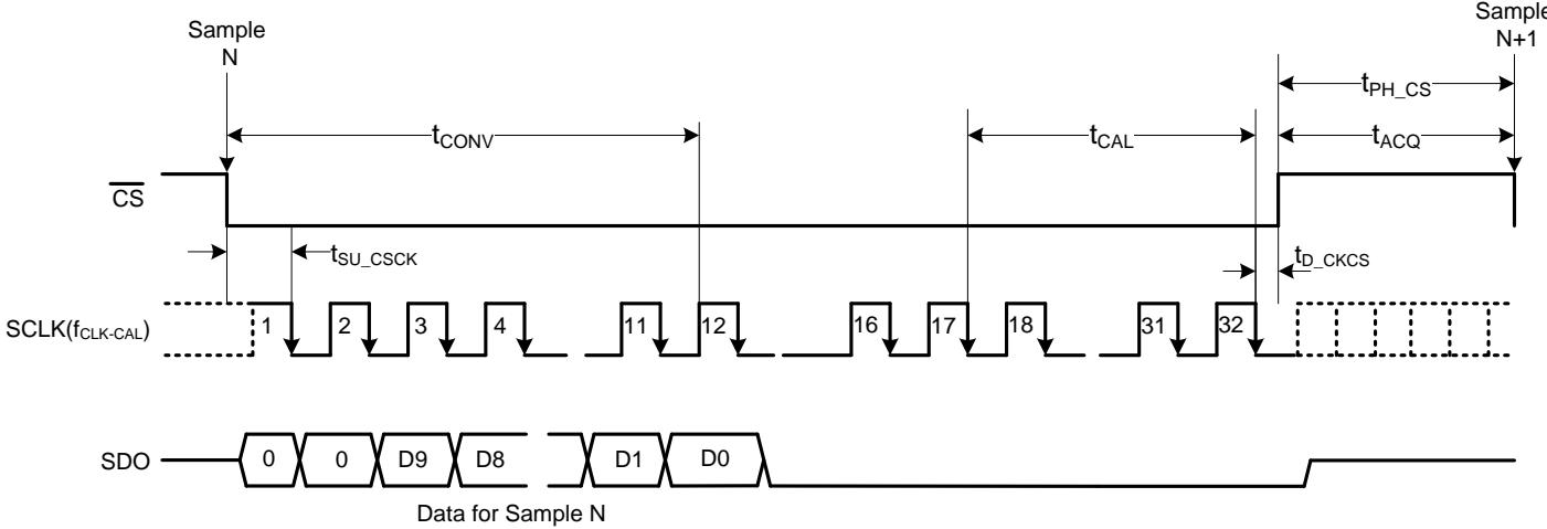
Figure 37. Offset Calibration During Normal Operation Timing Diagram
9 Application and Implementation
NOTE
Information in the following applications sections is not part of the TI component specification, and TI does not warrant its accuracy or completeness. TI’s customers are responsible for determining suitability of components for their purposes. Customers should validate and test their design implementation to confirm system functionality.
9.1 Application Information
The two primary circuits required to maximize the performance of a SAR ADC are the input driver and the reference driver circuits. This section details some general principles for designing the input driver circuit, reference driver circuit, and provides some application circuits designed for the ADS7039-Q1.
9.2 Typical Application

Figure 38. Single-Supply DAQ with the ADS7039-Q1
9.2.1 Design Requirements
The goal of this application is to design a single-supply digital acquisition (DAQ) circuit based on the ADS7039- Q1 with SNR greater than 61 dB and THD less than –75 dB for input frequencies of 2 kHz at a throughput of 2 MSPS.
9.2.2 Detailed Design Procedure
The input driver circuit for a high-precision ADC mainly consists of two parts: a driving amplifier and a charge kickback filter. Careful design of the front-end circuit is critical to meet the linearity and noise performance of a high-precision ADC.
Typical Application (continued)
9.2.2.1 Low Distortion Charge Kickback Filter Design
Figure 39 shows the input circuit of a typical SAR ADC. During the acquisition phase, the SW switch closes and connects the sampling capacitor $( \mathsf { C } _ { \mathsf { S H } } )$ to the input driver circuit. This action introduces a transient on the input pins of the SAR ADC. An ideal amplifier with 0 Ω of output impedance and infinite current drive can settle this transient in zero time. For a real amplifier with non-zero output impedance and finite drive strength, this switched capacitor load can create stability issues.
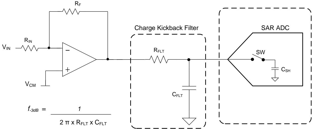
Figure 39. Charge Kickback Filter
For ac signals, the filter bandwidth must be kept low to band limit the noise fed into the ADC input, thereby increasing the SNR of the system. Besides filtering the noise from the front-end drive circuitry, the RC filter also helps attenuate the sampling charge injection from the switched-capacitor input stage of the ADC. A filter capacitor, $\complement _ { \mathsf { F L T } }$ , is connected across the ADC inputs. This capacitor helps reduce the sampling charge injection and provides a charge bucket to quickly charge the internal sample-and-hold capacitors during the acquisition process. As a rule of thumb, the value of this capacitor is at least 20 times the specified value of the ADC sampling capacitance. For this device, the input sampling capacitance is equal to 15 pF. Thus, the value of $\complement _ { \mathsf { F L T } }$ is greater than 300 pF. Select a COG- or NPO-type capacitor because these capacitor types have a high-Q, low temperature coefficient, and stable electrical characteristics under varying voltages, frequency, and time.
Note that driving capacitive loads can degrade the phase margin of the input amplifiers, thus making the amplifier marginally unstable. To avoid amplifier stability issues, series isolation resistors $( \mathsf { R } _ { \mathsf { F L T } } )$ are used at the output of the amplifiers. A higher value of $\dot { \mathsf { R } } _ { \mathsf { F L T } }$ is helpful from the amplifier stability perspective, but adds distortion as a result of interactions with the nonlinear input impedance of the ADC. Distortion increases with source impedance, input signal frequency, and input signal amplitude. Therefore, the selection of $\mathsf { R } _ { \mathsf { F L T } }$ requires balancing the stability and distortion of the design.
The input amplifier bandwidth is typically much higher than the cutoff frequency of the antialiasing filter. Thus, a SPICE simulation is strongly recommended to be performed to confirm that the amplifier has more than $4 0 ^ { \circ }$ phase margin with the selected filter. Simulation is critical because even with high-bandwidth amplifiers, some amplifiers can require more bandwidth than others to drive similar filters.
Typical Application (continued)
9.2.2.2 Input Amplifier Selection
To achieve a SINAD greater than 61 dB, the operational amplifier must have high bandwidth in order to settle the input signal within the acquisition time of the ADC. The operational amplifier must have low noise to keep the total system noise below 20% of the input-referred noise of the ADC. For the application circuit illustrated in Figure 38, the OPA365-Q1 is selected for its high bandwidth (50 MHz) and low noise (4.5 nV/√Hz).
For a step-by-step design procedure for a low-power, small form-factor digital acquisition (DAQ) circuit based on similar SAR ADCs, see the Three 12-Bit Data Acquisition Reference Designs Optimized for Low Power and Ultra-Small Form Factor TI Precision Design.
9.2.2.3 Reference Circuit
The analog supply voltage of the device is also used as a voltage reference for conversion. The AVDD pin is recommended to be decoupled with a 3.3-µF, low-ESR ceramic capacitor.
9.2.3 Application Curve
Figure 40 shows the FFT plot for the ADS7039-Q1 with a 2-kHz input frequency used for the circuit in Figure 38.
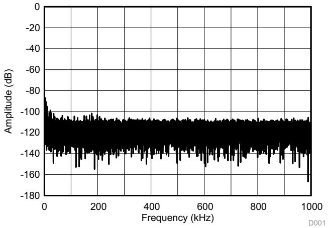
SNR = 70.6 dB, THD = –86 dB, SINAD = 70.2 dB, number of samples = 32768
Figure 40. Test Results for the ADS7039-Q1 and OPA365-Q1 for a 2-kHz Input
10 Power Supply Recommendations
10.1 AVDD and DVDD Supply Recommendations
The ADS7039-Q1 has two separate power supplies: AVDD and DVDD. The device operates on AVDD; DVDD is used for the interface circuits. AVDD and DVDD can be independently set to any value within the permissible ranges. The AVDD supply also defines the full-scale input range of the device. Always set the AVDD supply to be greater than or equal to the maximum input signal to avoid saturation of codes. Decouple the AVDD and DVDD pins individually with 3.3-µF ceramic decoupling capacitors, as shown in Figure 41.
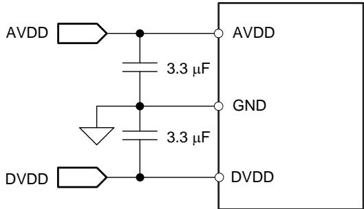
Figure 41. Power-Supply Decoupling
10.2 Estimating Digital Power Consumption
The current consumption from the DVDD supply depends on the DVDD voltage, load capacitance on the SDO line, and the output code. The load capacitance on the SDO line is charged by the current from the SDO pin on every rising edge of the data output and is discharged on every falling edge of the data output. The current consumed by the device from the DVDD supply can be calculated by Equation 3:
IDVDD = C × V × f
where:
• C = Load capacitance on the SDO line
• V = DVDD supply voltage and
• f = Number of transitions on the SDO output
(3)
The number of transitions on the SDO output depends on the output code, and thus changes with the analog input. The maximum value of f occurs when data output on SDO change at every SCLK. SDO data changing at every SCLK results in an output code of 3AAh or 155h. For an output code of 3AAh or 155h at a 2-MSPS throughput, the frequency of transitions on the SDO output is 10 MHz.
For the current consumption to remain at the lowest possible value, keep the DVDD supply at the lowest permissible value and keep the capacitance on the SDO line as low as possible.
10.3 Optimizing Power Consumed by the Device
• Keep the analog supply voltage (AVDD) as close as possible to the analog input voltage. Set AVDD to be greater than or equal to the analog input voltage of the device.
• Keep the digital supply voltage (DVDD) at the lowest permissible value.
• Reduce the load capacitance on the SDO output.
• Run the device at the optimum throughput. Power consumption reduces with throughput.
11 Layout
11.1 Layout Guidelines
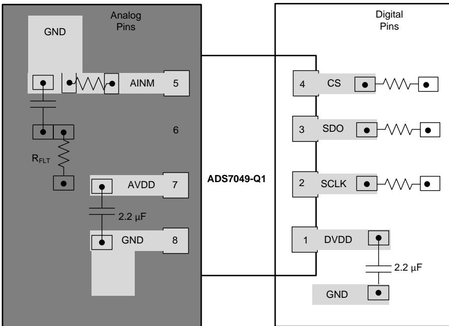
Figure 42 shows a board layout example for the ADS7039-Q1.
Some of the key considerations for an optimum layout with this device are:
• Use a ground plane underneath the device and partition the printed circuit board (PCB) into analog and digital sections.
• Avoid crossing digital lines with the analog signal path and keep the analog input signals and the reference input signals away from noise sources.
• The power sources to the device must be clean and well-bypassed. Use 2.2-μF ceramic bypass capacitors in close proximity to the analog (AVDD) and digital (DVDD) power-supply pins.
• Avoid placing vias between the AVDD and DVDD pins and the bypass capacitors.
• Connect ground pins to the ground plane using short, low-impedance path.
• Place the fly-wheel RC filters components close to the device.
Among ceramic surface-mount capacitors, COG (NPO) ceramic capacitors provide the best capacitance precision. The type of dielectric used in COG (NPO) ceramic capacitors provides the most stable electrical properties over voltage, frequency, and temperature changes.
11.2 Layout Example
Copyright © 2016, Texas Instruments Incorporated
Figure 42. Example Layout
12 Device and Documentation Support
12.1 Documentation Support
12.1.1 Related Documentation
For related documentation see the following:
• TPS732xx Capacitor-Free, NMOS, 250-mA Low-Dropout Regulator With Reverse Current Protection
Three 12-Bit Data Acquisition Reference Designs Optimized for Low Power and Ultra-Small Form Factor TI Precision Design
• OPAx314 3-MHz, Low-Power, Low-Noise, RRIO, 1.8-V CMOS Operational Amplifier
• OPAx365-Q1 50-MHz Low-Distortion High-CMRR Rail-to-Rail I/O, Single-Supply Operational Amplifiers
12.2 Receiving Notification of Documentation Updates
To receive notification of documentation updates, navigate to the device product folder on ti.com. In the upper right corner, click on Alert me to register and receive a weekly digest of any product information that has changed. For change details, review the revision history included in any revised document.
12.3 Community Resources
The following links connect to TI community resources. Linked contents are provided "AS IS" by the respective contributors. They do not constitute TI specifications and do not necessarily reflect TI's views; see TI's Terms of Use.
TI E2E™ Online Community TI's Engineer-to-Engineer (E2E) Community. Created to foster collaboration among engineers. At e2e.ti.com, you can ask questions, share knowledge, explore ideas and help solve problems with fellow engineers.
Design Support TI's Design Support Quickly find helpful E2E forums along with design support tools and contact information for technical support.
12.4 Trademarks
E2E is a trademark of Texas Instruments.
All other trademarks are the property of their respective owners.
12.5 Electrostatic Discharge Caution

This integrated circuit can be damaged by ESD. Texas Instruments recommends that all integrated circuits be handled with appropriate precautions. Failure to observe proper handling and installation procedures can cause damage.
ESD damage can range from subtle performance degradation to complete device failure. Precision integrated circuits may be more susceptible to damage because very small parametric changes could cause the device not to meet its published specifications.
12.6 Glossary
SLYZ022 — TI Glossary.
This glossary lists and explains terms, acronyms, and definitions.
13 Mechanical, Packaging, and Orderable Information
The following pages include mechanical packaging and orderable information. This information is the most current data available for the designated devices. This data is subject to change without notice and revision of this document. For browser-based versions of this data sheet, refer to the left-hand navigation.
PACKAGING INFORMATION
| Orderable part number | Status(1) | Material type(2) | Package | Pins | Package qty | Carrier | RoHS(3) | Lead finish/ Ball material(4) | MSL rating/ Peak reflow(5) | Op temp (°C) | Part marking(6) |
| ADS7039QDCURQ1 | Active | Production | VSSOP (DCU) | 8 | 3000 | LARGE T&R | Yes | NIPDAU | Level-2-260C-1 YEAR | -40 to 125 | 17UT |
| ADS7039QDCURQ1.A | Active | Production | VSSOP (DCU) | 8 | 3000 | LARGE T&R | Yes | NIPDAU | Level-2-260C-1 YEAR | -40 to 125 | 17UT |
(1) Status: For more details on status, see our product life cycle.
(2) Material type: When designated, preproduction parts are prototypes/experimental devices, and are not yet approved or released for full production. Testing and final process, including without limitation quality assurance, reliability performance testing, and/or process qualification, may not yet be complete, and this item is subject to further changes or possible discontinuation. If available for ordering, purchases will be subject to an additional waiver at checkout, and are intended for early internal evaluation purposes only. These items are sold without warranties of any kind.
(3) RoHS values: Yes, No, RoHS Exempt. See the TI RoHS Statement for additional information and value definition.
(4) Lead finish/Ball material: Parts may have multiple material finish options. Finish options are separated by a vertical ruled line. Lead finish/Ball material values may wrap to two lines if the finish value exceeds the maximum column width.
(5) MSL rating/Peak reflow: The moisture sensitivity level ratings and peak solder (reflow) temperatures. In the event that a part has multiple moisture sensitivity ratings, only the lowest level per JEDEC standards is shown. Refer to the shipping label for the actual reflow temperature that will be used to mount the part to the printed circuit board.
(6) Part marking: There may be an additional marking, which relates to the logo, the lot trace code information, or the environmental category of the part.
Multiple part markings will be inside parentheses. Only one part marking contained in parentheses and separated by a "~" will appear on a part. If a line is indented then it is a continuation of the previous line and the two combined represent the entire part marking for that device.
Important Information and Disclaimer:The information provided on this page represents TI's knowledge and belief as of the date that it is provided. TI bases its knowledge and belief on information provided by third parties, and makes no representation or warranty as to the accuracy of such information. Efforts are underway to better integrate information from third parties. TI has taken and continues to take reasonable steps to provide representativ and accurate information but may not have conducted destructive testing or chemical analysis on incoming materials and chemicals. TI and TI suppliers consider certain information to be proprietary, and thus CAS number and other limited information may not be available for release.
In no event shall TI's liability arising out of such information exceed the total purchase price of the TI part(s) at issue in this document sold by TI to Customer on an annual basis.
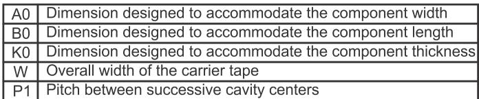
TAPE AND REEL INFORMATION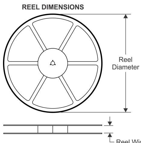
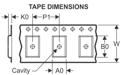
| A0 | Dimension designed to accommodate the component width |
| B0 | Dimension designed to accommodate the component length |
| K0 | Dimension designed to accommodate the component thickness |
| W | Overall width of the carrier tape |
| P1 | Pitch between successive cavity centers |
- Reel Width (W1)
QUADRANT ASSIGNMENTS FOR PIN 1 ORIENTATION IN TAPE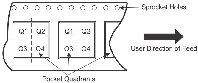
*All dimensions are nomina
| Device | Package Type | Package Drawing | Pins | SPQ | Reel Diameter (mm) | Reel Width W1 (mm) | A0 (mm) | B0 (mm) | K0 (mm) | P1 (mm) | W (mm) | Pin1 Quadrant |
| ADS7039QDCURQ1 | VSSOP | DCU | 8 | 3000 | 180.0 | 8.4 | 2.25 | 3.35 | 1.05 | 4.0 | 8.0 | Q3 |

*All dimensions are nomina
| Device | Package Type | Package Drawing | Pins | SPQ | Length (mm) | Width (mm) | Height (mm) |
| ADS7039QDCURQ1 | VSSOP | DCU | 8 | 3000 | 223.0 | 270.0 | 35.0 |
SMALL OUTLINE PACKAGE
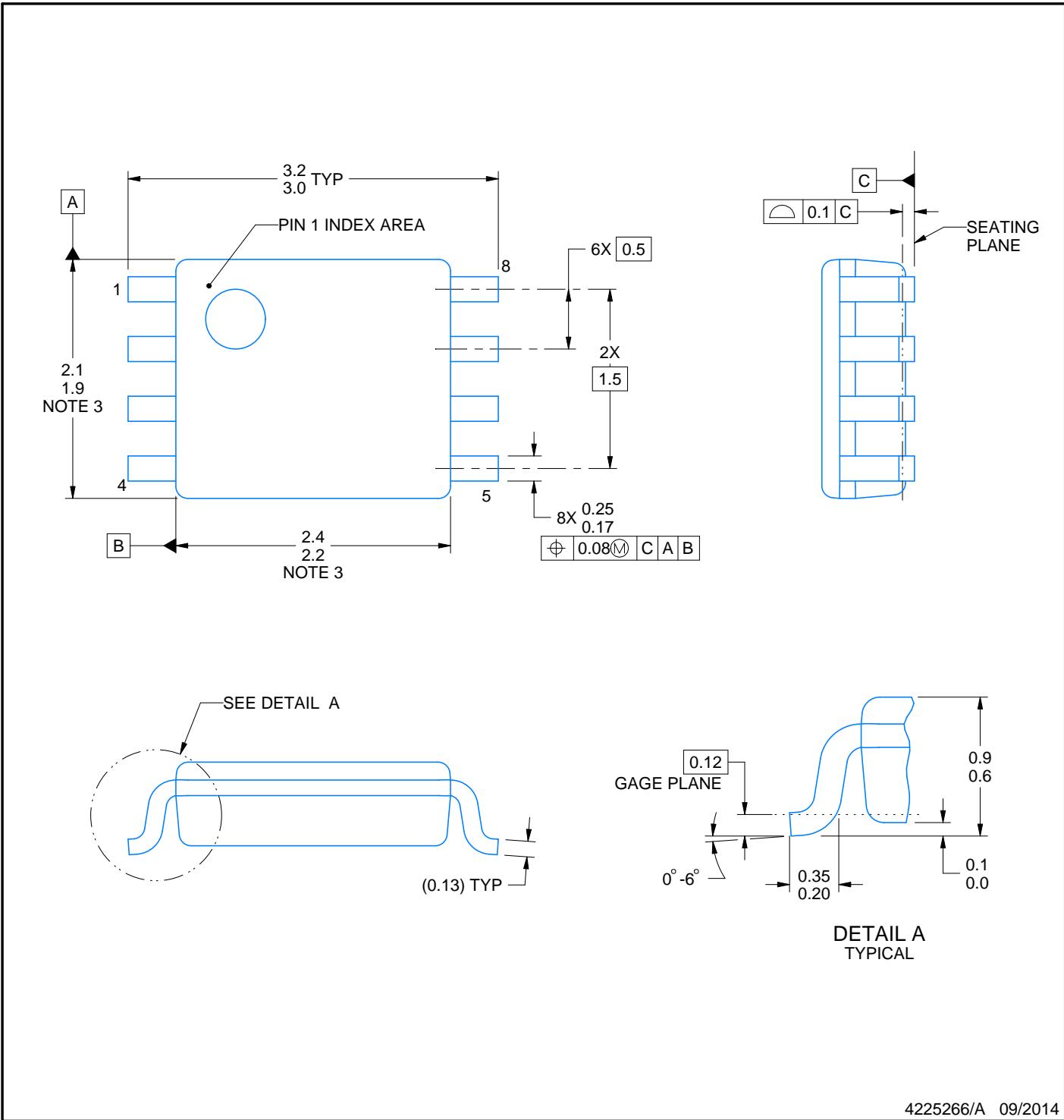
4225266/A 09/2014
NOTES:
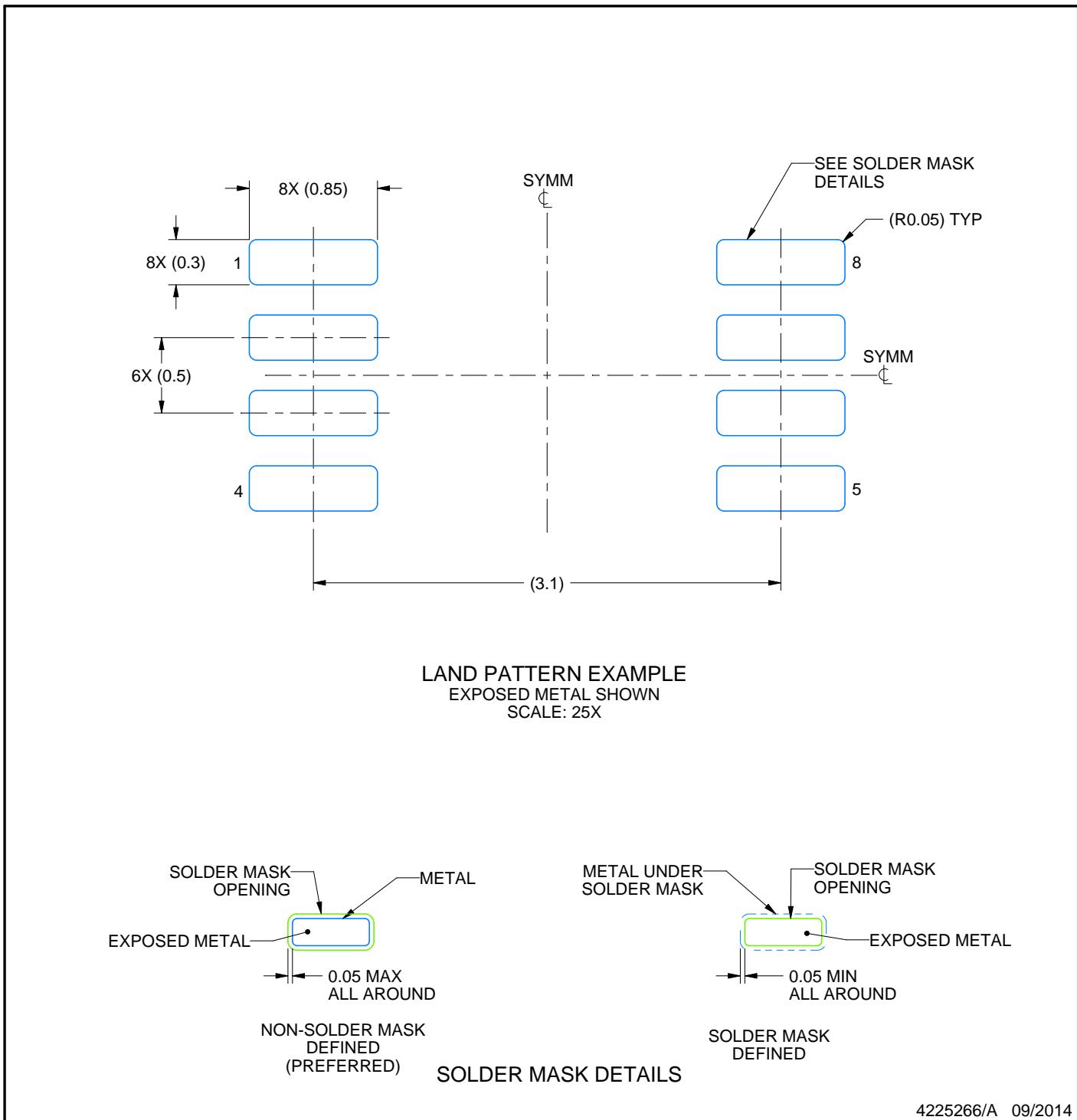
NOTES: (continued)
Publication IPC-7351 may have alternate designs.
Solder mask tolerances between and around signal pads can vary based on board fabrication site.
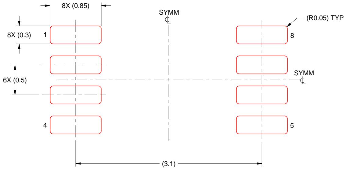
(R0.05) TYP
SOLDER PASTE EXAMPLE BASED ON 0.125 mm THICK STENCIL SCALE: 25X
4225266/A 09/2014
NOTES: (continued)
Laser cutting apertures with trapezoidal walls and rounded corners may offer better paste release. IPC-7525 may have alternate design recommendations.
Board assembly site may have different recommendations for stencil design.
Figures and diagrams from the PDF
Preview the extracted datasheet assets and open any image in a separate tab for closer inspection.











Use this datasheet from any agent
Send the page, markdown, chunks, or search endpoint to ChatGPT, Claude, embedr-app, or your own tooling.