
Texas Instruments DRV8876PWPR H-Bridge Motor Driver
Texas Instruments DRV8876PWPR 40-V, 3.5-A brushed-DC H-bridge motor-driver IC with integrated current sense/current regulation, IPROPI current feedback, and open-drain nFAULT in the PWP HTSSOP-16 PowerPAD package.
DRV8876 H-Bridge Motor Driver With Integrated Current Sense and Regulation
1 Features
1• N-channel H-bridge motor driver
– Drives one bidirectional brushed DC motor
– Two unidirectional brushed DC motors
– Other resistive and inductive loads
• 4.5-V to 37-V operating supply voltage range
• Pin to pin ${ \mathsf { R } } _ { \mathsf { D S } ( \mathsf { o n } ) }$ variants
– DRV8874: 200-mΩ (High-Side + Low-Side)
– DRV8876: 700-mΩ (High-Side + Low-Side)
• High output current capability
– DRV8874: 6-A Peak
– DRV8876: 3.5-A Peak
• Integrated current sensing and regulation
• Proportional current output (IPROPI)
• Selectable current regulation (IMODE) – Cycle-by-cycle or fixed off time
• Selectable input control modes (PMODE)
– PH/EN and PWM H-bridge control modes
– Independent half-bridge control mode
• Supports 1.8-V, 3.3-V, and 5-V logic inputs
• Ultra low-power sleep mode
$$
- < 1 - \mu A @ V _ {V M} = 2 4 - V, T _ {J} = 2 5 ^ {\circ} C
$$
• Spread spectrum clocking for low electromagnetic interference (EMI)
• Integrated protection features
– Undervoltage lockout (UVLO)
– Charge pump undervoltage (CPUV)
– Overcurrent protection (OCP)
– Automatic retry or outputs latched off (IMODE)
– Thermal shutdown (TSD)
– Automatic fault recovery
– Fault indicator pin (nFAULT)
2 Applications
Brushed DC motors
• Major and small home appliances
• Vacuum, humanoid, and toy robotics
• Printers and scanners
• Smart meters
• ATMs, currency counters, and EPOS
• Servo motors and actuators
3 Description
The DRV887x family of devices are flexible motor drivers for a wide variety of applications. The devices integrate an N-channel H-bridge, charge pump regulator, current sensing and regulation, current proportional output, and protection circuitry. The charge pump improves efficiency by allowing for both high-side and low-side N-channels MOSFETs and 100% duty cycle support. The family of devices come in pin-to-pin, scalable ${ \mathsf { R } } _ { \mathsf { D S ( o n ) } }$ options to support different loads with minimal design changes.
Integrated current sensing allows for the driver to regulate the motor current during start up and high load events. A current limit can be set with an adjustable external voltage reference. Additionally, the devices provide an output current proportional to the motor load current. This can be used to detect motor stall or change in load conditions. The integrated current sensing uses an internal current mirror architecture, removing the need for a large power shunt resistor, saving board area and reducing system cost.
A low-power sleep mode is provided to achieve ultralow quiescent current draw by shutting down most of the internal circuitry. Internal protection features are provided for supply undervoltage lockout (UVLO), charge pump undervoltage (CPUV), output overcurrent (OCP), and device overtemperature (TSD). Fault conditions are indicated on nFAULT.
Device Information (1)
| PART NUMBER | PACKAGE | BODY SIZE (NOM) |
| DRV8876 | HTSSOP (16) | 5.00 mm × 4.40 mm |
| VQFN (16) | 3.00 mm × 3.00 mm |
(1) For all available packages, see the orderable addendum at the end of the data sheet.
Simplified Schematic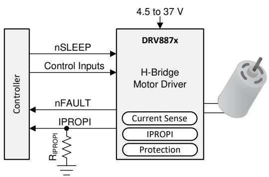
Table of Contents
1 Features.... 1
2 Applications.... 1
3 Description.... 1
4 Revision History.... 2
5 Pin Configuration and Functions.... 3
6 Specifications.... 4
6.1 Absolute Maximum Ratings.... 4
6.2 ESD Ratings.... 4
6.3 Recommended Operating Conditions.... 4
6.4 Thermal Information.... 5
6.5 Electrical Characteristics.... 5
6.6 Typical Characteristics.... 7
7 Detailed Description.... 9
7.1 Overview.... 9
7.2 Functional Block Diagram.... 9
7.3 Feature Description.... 10
7.4 Device Functional Modes.... 17
8 Application and Implementation.... 19
8.1 Application Information.... 19
8.2 Typical Application.... 19
9 Power Supply Recommendations.... 31
9.1 Bulk Capacitance.... 31
10 Layout.... 32
10.1 Layout Guidelines.... 32
10.2 Layout Example.... 32
11 Device and Documentation Support.... 34
11.1 Documentation Support.... 34
11.2 Receiving Notification of Documentation Updates.... 34
11.3 Community Resources.... 34
11.4 Trademarks.... 34
11.5 Electrostatic Discharge Caution.... 34
11.6 Glossary.... 34
12 Mechanical, Packaging, and Orderable Information.... 35
4 Revision History
Changes from Original (October 2018) to Revision A Page
• Changed device status to Production Data .... 1
Changes from Revision A (April 2019) to Revision B Page
• Added load condition to $t_{PD}$ test conditions .... 6
• Added PWP package designator to $A_{ERR}$ test conditions.... 6
5 Pin Configuration and Functions
DRV8876 RGT Package 16-Pin VQFN With Exposed Thermal Pad Top View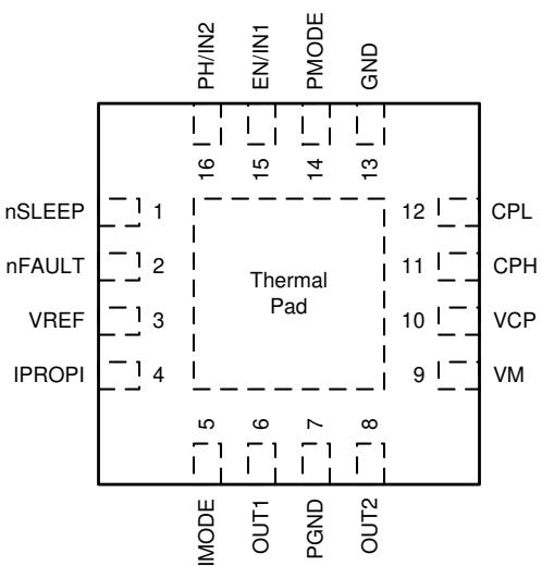
DRV8876 PWP Package 16-Pin HTSSOP With Exposed Thermal Pad Top View
| EN/IN1 | 1 | Thermal Pad | 16 | PMODE |
| PH/IN2 | 2 | 15 | GND | |
| nSLEEP | 3 | 14 | CPL | |
| nFAULT | 4 | 13 | CPH | |
| VREF | 5 | 12 | VCP | |
| IPROPI | 6 | 11 | VM | |
| IMODE | 7 | 10 | OUT2 | |
| OUT1 | 8 | 9 | PGND |
Pin Functions
| PIN | TYPE(1) | DESCRIPTION | ||
| NAME | RGT | PWP | ||
| CPH | 11 | 13 | PWR | Charge pump switching node. Connect a X5R or X7R, 22-nF, VM-rated ceramic capacitor between the CPH and CPL pins. |
| CPL | 12 | 14 | PWR | |
| EN/IN1 | 15 | 1 | I | H-bridge control input. See Control Modes. Internal pulldown resistor. |
| GND | 13 | 15 | PWR | Device ground. Connect to system ground. |
| IMODE | 5 | 7 | I | Current regulation and overcurrent protection mode. See Current Regulation. Quad-level input. |
| IPROPI | 4 | 6 | O | Analog current output proportional to load current. See Current Sensing. |
| nFAULT | 2 | 4 | OD | Fault indicator output. Pulled low during a fault condition. Connect an external pullup resistor for open-drain operation. See Protection Circuits. |
| nSLEEP | 1 | 3 | I | Sleep mode input. Logic high to enable device. Logic low to enter low-power sleep mode. See Device Functional Modes. Internal pulldown resistor. |
| OUT1 | 6 | 8 | O | H-bridge output. Connect to the motor or other load. |
| OUT2 | 8 | 10 | O | H-bridge output. Connect to the motor or other load. |
| PGND | 7 | 9 | PWR | Device power ground. Connect to system ground. |
| PH/IN2 | 16 | 2 | I | H-bridge control input. See Control Modes. Internal pulldown resistor. |
| PMODE | 14 | 16 | I | H-bridge control input mode. See Control Modes. Tri-level input. |
| VCP | 10 | 12 | PWR | Charge pump output. Connect a X5R or X7R, 100-nF, 16-V ceramic capacitor between the VCP and VM pins. |
| VM | 9 | 11 | PWR | 4.5-V to 37-V power supply input. Connect a 0.1-μF bypass capacitor to ground, as well as sufficient Bulk Capacitance rated for VM. |
| VREF | 3 | 5 | I | External reference voltage input to set internal current regulation limit. See Current Regulation. |
| PAD | — | — | — | Thermal pad. Connect to system ground. |
(1) PWR = power, I = input, O = output, NC = no connection, OD = open-drain
6 Specifications
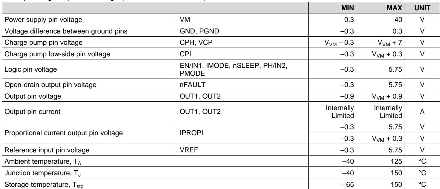
6.1 Absolute Maximum Ratings
over operating temperature range (unless otherwise noted)(1)
| MIN | MAX | UNIT | ||
| Power supply pin voltage | VM | -0.3 | 40 | V |
| Voltage difference between ground pins | GND, PGND | -0.3 | 0.3 | V |
| Charge pump pin voltage | CPH, VCP | $V_{VM} - 0.3$ | $V_{VM} + 7$ | V |
| Charge pump low-side pin voltage | CPL | -0.3 | $V_{VM} + 0.3$ | V |
| Logic pin voltage | EN/IN1, IMODE, nSLEEP, PH/IN2, PMODE | -0.3 | 5.75 | V |
| Open-drain output pin voltage | nFAULT | -0.3 | 5.75 | V |
| Output pin voltage | OUT1, OUT2 | -0.9 | $V_{VM} + 0.9$ | V |
| Output pin current | OUT1, OUT2 | Internally Limited | Internally Limited | A |
| Proportional current output pin voltage | IPROPI | -0.3 | 5.75 | V |
| -0.3 | $V_{VM} + 0.3$ | V | ||
| Reference input pin voltage | VREF | -0.3 | 5.75 | V |
| Ambient temperature, $T_A$ | -40 | 125 | °C | |
| Junction temperature, $T_J$ | -40 | 150 | °C | |
| Storage temperature, $T_{stg}$ | -65 | 150 | °C | |
(1) Stresses beyond those listed under Absolute Maximum Rating may cause permanent damage to the device. These are stress ratings only, which do not imply functional operation of the device at these or any other conditions beyond those indicated under Recommended Operating Condition. Exposure to absolute-maximum-rated conditions for extended periods may affect device reliability.
6.2 ESD Ratings
| VALUE | UNIT | |||
| $V_{(ESD)}$ | Electrostatic discharge | Human body model (HBM), per ANSI/ESDA/JEDEC JS-001 $^{(1)}$ | ±2000 | V |
| Charged device model (CDM), per JEDEC specification JESD22-C101 $^{(2)}$ | ±500 | |||
(1) JEDEC document JEP155 states that 500-V HBM allows safe manufacturing with a standard ESD control process. Pins listed $a \mathbf { s } \pm 2 0 0 0$ V may actually have higher performance.
(2) JEDEC document JEP157 states that 250-V CDM allows safe manufacturing with a standard ESD control process. Pins listed as ± 500 V may actually have higher performance.
6.3 Recommended Operating Conditions
over operating temperature range (unless otherwise noted)
| MIN | NOM | MAX | UNIT | |||
| $V_{VM}$ | Power supply voltage | VM | 4.5 | 37 | V | |
| $V_{IN}$ | Logic input voltage | EN/IN1, MODE, nSLEEP, PH/IN2 | 0 | 5.5 | V | |
| $f_{PWM}$ | PWM frequency | EN/IN1, PH/IN2 | 0 | 100 | kHz | |
| $V_{OD}$ | Open drain pullup voltage | nFAULT | 0 | 5.5 | V | |
| $I_{OD}$ | Open drain output current | nFAULT | 0 | 5 | mA | |
| $I_{OUT}^{(1)}$ | Peak output current | OUT1, OUT2 | 0 | 3.5 | A | |
| $I_{IPROPI}$ | Current sense output current | IPROPI | 0 | 3 | mA | |
| $V_{VREF}$ | Current limit reference voltage | VREF | 0 | 3.6 | V | |
| $T_A$ | Operating ambient temperature | -40 | 125 | °C | ||
| $T_J$ | Operating junction temperature | -40 | 150 | °C | ||
(1) Power dissipation and thermal limits must be observed
6.4 Thermal Information
| THERMAL METRIC(1) | DRV8876 | DRV8876 | UNIT | |
| RGT (VQFN) | PWP (HTSSOP) | |||
| 16 PINS | 16 PINS | |||
| $R_{\theta JA}$ | Junction-to-ambient thermal resistance | 45.9 | 44.3 | °C/W |
| $R_{\theta JC(top)}$ | Junction-to-case (top) thermal resistance | 48.8 | 38.3 | °C/W |
| $R_{\theta JB}$ | Junction-to-board thermal resistance | 19.9 | 20.5 | °C/W |
| $\Psi_{JT}$ | Junction-to-top characterization parameter | 1.1 | 1.0 | °C/W |
| $\Psi_{JB}$ | Junction-to-board characterization parameter | 19.9 | 20.4 | °C/W |
| $R_{\theta JC(bot)}$ | Junction-to-case (bottom) thermal resistance | 7.1 | 5.0 | °C/W |
(1) For more information about traditional and new thermal metrics, see the Semiconductor and IC Package Thermal Metrics application report.
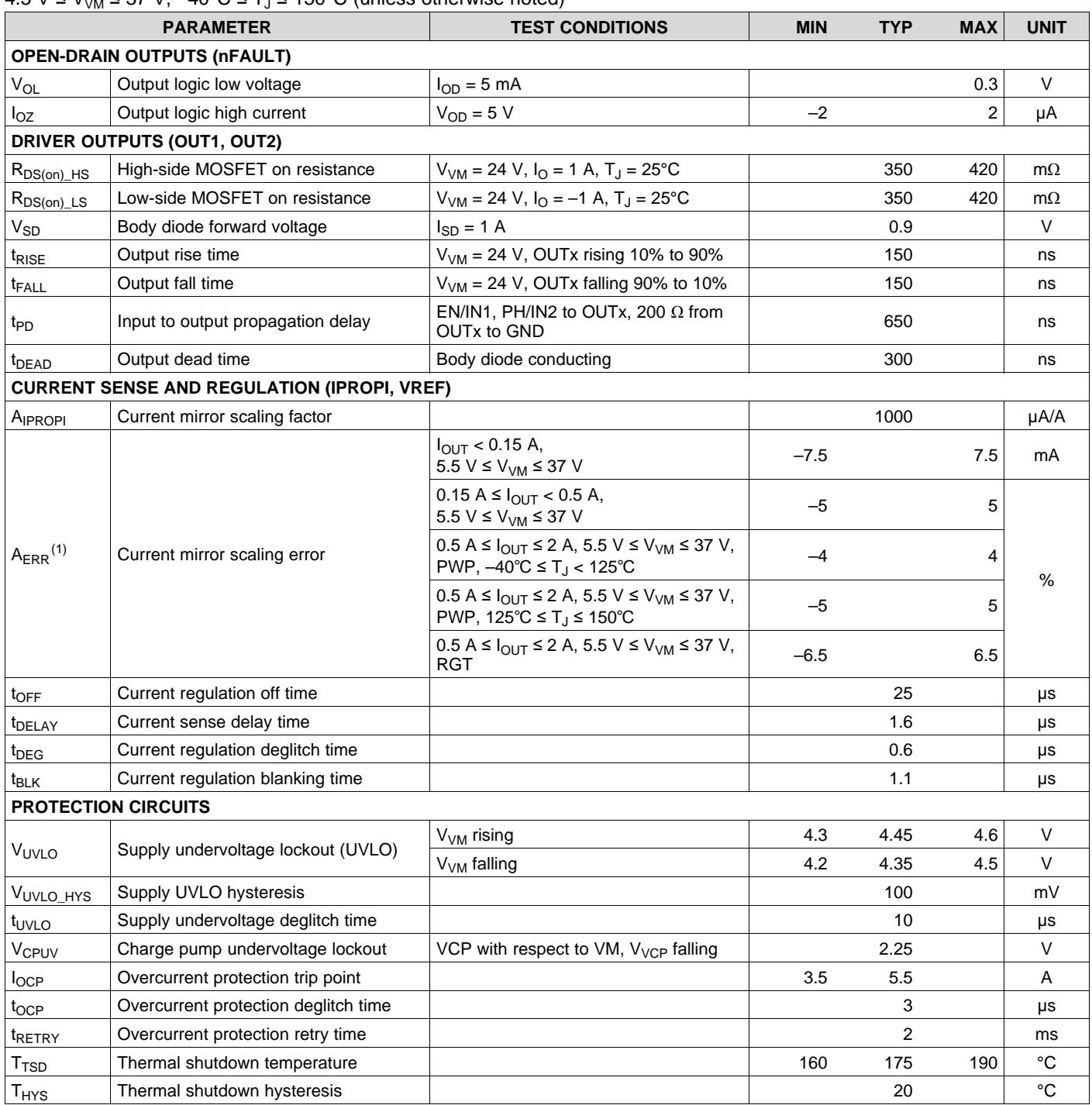
6.5 Electrical Characteristics
4.5 $\vee \le \vee _ { \vee \mathbb { M } } \le 3 7 \vee , - 4 0 ^ { \circ } \mathbb { C } \le \mathsf { T } _ { \mathsf { J } } \le 1 5 0 ^ { \circ } \mathbb { C }$ (unless otherwise noted)
| PARAMETER | TEST CONDITIONS | MIN | TYP | MAX | UNIT | |
| POWER SUPPLIES (VCP, VM) | ||||||
| $I_{VMQ}$ | VM sleep mode current | $V_{VM}=24 V, nSLEEP=0 V, T_J=25°C$ | 0.75 | 1 | μA | |
| nSLEEP=0 V | 5 | μA | ||||
| $I_{VM}$ | VM active mode current | $V_{VM}=24 V, nSLEEP=5 V, EN/IN1=PH/IN2=0 V$ | 3 | 7 | mA | |
| $t_{WAKE}$ | Turnon time | $V_{VM}>V_{UVLO}, nSLEEP=5 V to active$ | 1 | ms | ||
| $t_{SLEEP}$ | Turnoff time | nSLEEP=0 V to sleep mode | 1 | ms | ||
| $V_{VCP}$ | Charge pump regulator voltage | VCP with respect to VM, $V_{VM}=24 V$ | 5 | V | ||
| $f_{VCP}$ | Charge pump switching frequency | 400 | kHz | |||
| LOGIC-LEVEL INPUTS (EN/IN1, PH/IN2, nSLEEP) | ||||||
| $V_{IL}$ | Input logic low voltage | $V_{VM}<5 V$ | 0 | 0.7 | V | |
| $V_{VM}≥5 V$ | 0 | 0.8 | ||||
| $V_{IH}$ | Input logic high voltage | 1.5 | 5.5 | V | ||
| $V_{HYS}$ | Input hysteresis | 200 | mV | |||
| nSLEEP | 50 | mV | ||||
| $I_{IL}$ | Input logic low current | $V_I=0 V$ | -5 | 5 | μA | |
| $I_{IH}$ | Input logic high current | $V_I=5 V$ | 50 | 75 | μA | |
| $R_{PD}$ | Input pulldown resistance | To GND | 100 | kΩ | ||
| TRI-LEVEL INPUTS (PMODE) | ||||||
| $V_{TIL}$ | Tri-level input logic low voltage | 0 | 0.65 | V | ||
| $V_{TIZ}$ | Tri-level input Hi-Z voltage | 0.9 | 1.1 | 1.2 | V | |
| $V_{TIH}$ | Tri-level input logic high voltage | 1.5 | 5.5 | V | ||
| $I_{TIL}$ | Tri-level input logic low current | $V_I=0 V$ | -50 | -32 | μA | |
| $I_{TIZ}$ | Tri-level input Hi-Z current | $V_I=1.1 V$ | -5 | 5 | μA | |
| $I_{TIH}$ | Tri-level input logic high current | $V_I=5 V$ | 113 | 150 | μA | |
| $R_{TPD}$ | Tri-level pulldown resistance | To GND | 44 | kΩ | ||
| $R_{TPU}$ | Tri-level pullup resistance | To internal 5 V | 156 | kΩ | ||
| QUAD-LEVEL INPUTS (IMODE) | ||||||
| $V_{QI2}$ | Quad-level input level 1 | Voltage to set quad-level 1 | 0 | 0.45 | V | |
| $R_{QI2}$ | Quad-level input level 2 | Resistance to GND to set quad-level 2 | 18.6 | 20 | 21.4 | kΩ |
| $R_{QI3}$ | Quad-level input level 3 | Resistance to GND to set quad-level 3 | 57.6 | 62 | 66.4 | kΩ |
| $V_{QI4}$ | Quad-level input level 4 | Voltage to set quad-level 4 | 2.5 | 5.5 | V | |
| $R_{QPD}$ | Quad-level pulldown resistance | To GND | 136 | kΩ | ||
| $R_{QPU}$ | Quad-level pullup resistance | To internal 5 V | 68 | kΩ | ||
Electrical Characteristics (continued)
4.5 $\vee \le \vee _ { \vee \mathbb { M } } \le 3 7 \vee , - 4 0 ^ { \circ } \mathbb { C } \le \mathsf { T } _ { \mathsf { J } } \le 1 5 0 ^ { \circ } \mathbb { C }$ (unless otherwise noted)
| PARAMETER | TEST CONDITIONS | MIN | TYP | MAX | UNIT | |
| OPEN-DRAIN OUTPUTS (nFAULT) | ||||||
| $V_{OL}$ | Output logic low voltage | $I_{OD}=5 mA$ | 0.3 | V | ||
| $I_{OZ}$ | Output logic high current | $V_{OD}=5 V$ | -2 | 2 | μA | |
| DRIVER OUTPUTS (OUT1, OUT2) | ||||||
| $R_{DS(on)_HS}$ | High-side MOSFET on resistance | $V_{VM}=24 V, I_{O}=1 A, T_{J}=25°C$ | 350 | 420 | mΩ | |
| $R_{DS(on)_LS}$ | Low-side MOSFET on resistance | $V_{VM}=24 V, I_{O}=-1 A, T_{J}=25°C$ | 350 | 420 | mΩ | |
| $V_{SD}$ | Body diode forward voltage | $I_{SD}=1 A$ | 0.9 | V | ||
| $t_{RISE}$ | Output rise time | $V_{VM}=24 V, OUTx rising 10% to 90%$ | 150 | ns | ||
| $t_{FALL}$ | Output fall time | $V_{VM}=24 V, OUTx falling 90% to 10%$ | 150 | ns | ||
| $t_{PD}$ | Input to output propagation delay | EN/IN1, PH/IN2 to OUTx, 200 Ω from OUTx to GND | 650 | ns | ||
| $t_{DEAD}$ | Output dead time | Body diode conducting | 300 | ns | ||
| CURRENT SENSE AND REGULATION (IPROPI, VREF) | ||||||
| $A_{IPROPI}$ | Current mirror scaling factor | 1000 | μA/A | |||
| $A_{ERR}^{(1)}$ | Current mirror scaling error | $I_{OUT}<0.15 A, 5.5 V ≤ V_{VM} ≤ 37 V$ | -7.5 | 7.5 | mA | |
| 0.15 A ≤ $I_{OUT}<0.5 A, 5.5 V ≤ V_{VM} ≤ 37 V$ | -5 | 5 | % | |||
| 0.5 A ≤ $I_{OUT}≤2 A, 5.5 V ≤ V_{VM} ≤ 37 V, PWP, -40°C ≤ T_{J}<125°C$ | -4 | 4 | ||||
| 0.5 A ≤ $I_{OUT}≤2 A, 5.5 V ≤ V_{VM} ≤ 37 V, PWP, 125°C ≤ T_{J}≤150°C$ | -5 | 5 | ||||
| 0.5 A ≤ $I_{OUT}≤2 A, 5.5 V ≤ V_{VM} ≤ 37 V, RGT$ | -6.5 | 6.5 | ||||
| $t_{OFF}$ | Current regulation off time | 25 | μs | |||
| $t_{DELAY}$ | Current sense delay time | 1.6 | μs | |||
| $t_{DEG}$ | Current regulation deglitch time | 0.6 | μs | |||
| $t_{BLK}$ | Current regulation blanking time | 1.1 | μs | |||
| PROTECTION CIRCUITS | ||||||
| $V_{UVLO}$ | Supply undervoltage lockout (UVLO) | $V_{VM}$ rising | 4.3 | 4.45 | 4.6 | V |
| $V_{VM}$ falling | 4.2 | 4.35 | 4.5 | V | ||
| $V_{UVLO_HYS}$ | Supply UVLO hysteresis | 100 | mV | |||
| $t_{UVLO}$ | Supply undervoltage deglitch time | 10 | μs | |||
| $V_{CPUV}$ | Charge pump undervoltage lockout | VCP with respect to VM, $V_{VCP}$ falling | 2.25 | V | ||
| $I_{OCP}$ | Overcurrent protection trip point | 3.5 | 5.5 | A | ||
| $t_{OCP}$ | Overcurrent protection deglitch time | 3 | μs | |||
| $t_{RETRY}$ | Overcurrent protection retry time | 2 | ms | |||
| $T_{TSD}$ | Thermal shutdown temperature | 160 | 175 | 190 | °C | |
| $T_{HYS}$ | Thermal shutdown hysteresis | 20 | °C | |||
(1) At low currents, the IPROPI output has a fixed offset error with respect to the I current through the low-side power MOSFETs.
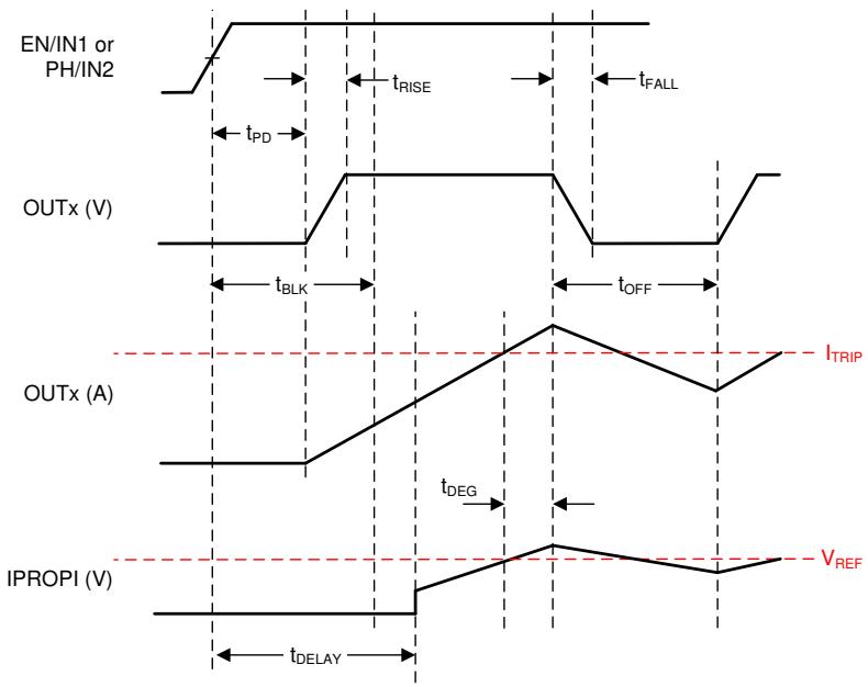
Figure 1. Timing Parameter Diagram
6.6 Typical Characteristics

Figure 2. Sleep Current (IVMQ) vs. Supply Voltage (VVM)
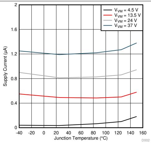
Figure 3. Sleep Current (I ) vs. Junction Temperature
Typical Characteristics (continued)
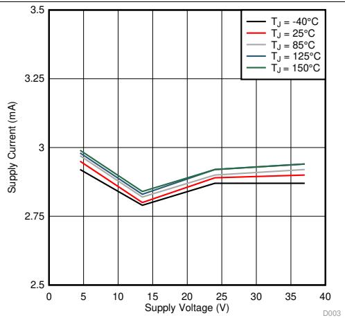

Figure 4. Active Current (IVM) vs. Supply Voltage (VVM)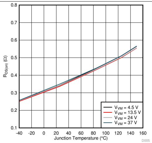
Figure 5. Active Current (IVM) vs. Junction Temperature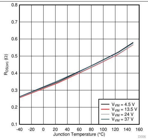
Figure 6. Low-Side $\mathsf { R } _ { \mathsf { D } \mathsf { S } ( \mathsf { o n } ) }$ vs. Junction Temperature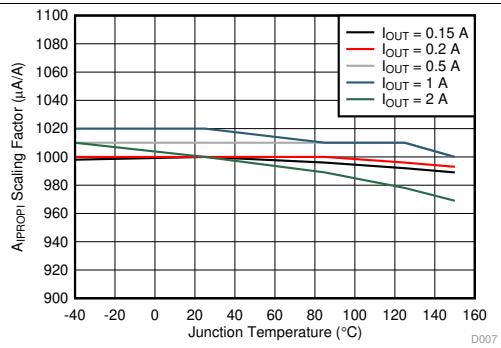
Figure 8. OUT1 Current Sense Error vs. Junction Temperature
Figure 7. High-Side $\mathsf { R } _ { \mathsf { D } \mathsf { S } ( \mathsf { o n } ) }$ vs. Junction Temperature
Figure 9. OUT2 Current Sense Error vs. Junction Temperature
7 Detailed Description
7.1 Overview
The DRV887x family of devices are brushed DC motor drivers that operate from 4.5 to 37-V supporting a wide range of output load currents for various types of motors and loads. The devices integrate an H-bridge output power stage that can be operated in different control modes set by the PMODE pin setting. This allows for driving a single bidirectional brushed DC motor, two unidirectional brushed DC motors, or other output load configurations. The devices integrate a charge pump regulator to support more efficient high-side N-channel MOSFETs and 100% duty cycle operation. The devices operate from a single power supply input (VM) which can be directly connected to a battery or DC voltage supply. The nSLEEP pin provides an ultra-low power mode to minimize current draw during system inactivity.
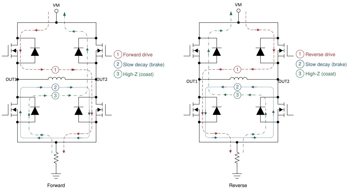
The DRV887x family of devices also integrate current sense output using current mirrors on the low-side power MOSFETs. The IPROPI pin sources a small current that is proportional to the current in the MOSFETs. This current can be converted to a proportional voltage using an external resistor $\scriptstyle \left( { \mathsf { R } } _ { | { \mathsf { P R O P l } } } \right)$ The integrated current sensing allows the DRV887x devices to limit the output current with a fixed off-time PWM chopping scheme and provide load information to the external controller to detect changes in load or stall conditions. The integrated current sensing out performs traditional external shunt resistor sensing by providing current information even during the off-time slow decay recirculating period and removing the need for an external power shunt resistor. The off-time PWM current regulation level can be configured during motor operation through the VREF pin to limit the load current accordingly to the system demands.
A variety of integrated protection features protect the device in the case of a system fault. These include undervoltage lockout (UVLO), charge pump undervoltage (CPUV), overcurrent protection (OCP), and overtemperature shutdown (TSD). Fault conditions are indicated on the nFAULT pin.
7.2 Functional Block Diagram

7.3 Feature Description
7.3.1 External Components
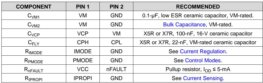
Table 1 lists the recommended external components for the device.
Table 1. Recommended External Components
| COMPONENT | PIN 1 | PIN 2 | RECOMMENDED |
| $C_{VM1}$ | VM | GND | 0.1-μF, low ESR ceramic capacitor, VM-rated. |
| $C_{VM2}$ | VM | GND | Bulk Capacitance, VM-rated. |
| $C_{VCP}$ | VCP | VM | X5R or X7R, 100-nF, 16-V ceramic capacitor |
| $C_{FLY}$ | CPH | CPL | X5R or X7R, 22-nF, VM-rated ceramic capacitor |
| $R_{IMODE}$ | IMODE | GND | See Current Regulation. |
| $R_{PMODE}$ | PMODE | GND | See Control Modes. |
| $R_{nFAULT}$ | VCC | nFAULT | Pullup resistor, $I_{OD} \leq 5$ -mA |
| $R_{IPROPI}$ | IPROPI | GND | See Current Sensing. |
7.3.2 Control Modes
The DRV887x family of devices provides three modes to support different control schemes with the EN/IN1 and PH/IN2 pins. The control mode is selected through the PMODE pin with either logic low, logic high, or setting the pin Hi-Z as shown in Table 2. The PMODE pin state is latched when the device is enabled through the nSLEEP pin. The PMODE state can be changed by taking the nSLEEP pin logic low, waiting the tSLEEP time, changing the PMODE pin input, and then enabling the device by taking the nSLEEP pin back logic high.
Table 2. PMODE Functions
| PMODE STATE | CONTROL MODE |
| PMODE = Logic Low | PH/EN |
| PMODE = Logic High | PWM |
| PMODE = Hi-Z | Independent Half-Bridge |
Figure 10. H-Bridge States
The inputs can accept static or pulse-width modulated (PWM) voltage signals for either 100% or PWM drive modes. The device input pins can be powered before VM is applied with no issues. By default, the EN/IN1 and PH/IN2 pins have an internal pulldown resistor to ensure the outputs are Hi-Z if no inputs are present.
The sections below show the truth table for each control mode. Note that these tables do not take into account the internal current regulation feature. Additionally, the DRV887x family of devices automatically handles the dead-time generation when switching between the high-side and low-side MOSFET of a half-bridge.
Figure 10 describes the naming and configuration for the various H-bridge states.
7.3.2.1 PH/EN Control Mode (PMODE = Logic Low)
When the PMODE pin is logic low on power up, the device is latched into PH/EN mode. PH/EN mode allows for the H-bridge to be controlled with a speed and direction type of interface. The truth table for PH/EN mode is shown in Table 3.
Table 3. PH/EN Control Mode
| nSLEEP | EN | PH | OUT1 | OUT2 | DESCRIPTION |
| 0 | X | X | Hi-Z | Hi-Z | Sleep, (H-Bridge Hi-Z) |
| 1 | 0 | X | L | L | Brake, (Low-Side Slow Decay) |
| 1 | 1 | 0 | L | H | Reverse (OUT2 → OUT1) |
| 1 | 1 | 1 | H | L | Forward (OUT1 → OUT2) |
7.3.2.2 PWM Control Mode (PMODE = Logic High)
When the PMODE pin is logic high on power up, the device is latched into PWM mode. PWM mode allows for the H-bridge to enter the Hi-Z state without taking the nSLEEP pin logic low. The truth table for PWM mode is shown in Table 4.
Table 4. PWM Control Mode
| nSLEEP | IN1 | IN2 | OUT1 | OUT2 | DESCRIPTION |
| 0 | X | X | Hi-Z | Hi-Z | Sleep, (H-Bridge Hi-Z) |
| 1 | 0 | 0 | Hi-Z | Hi-Z | Coast, (H-Bridge Hi-Z) |
| 1 | 0 | 1 | L | H | Reverse (OUT2 → OUT1) |
| 1 | 1 | 0 | H | L | Forward (OUT1 → OUT2) |
| 1 | 1 | 1 | L | L | Brake, (Low-Side Slow Decay) |
7.3.2.3 Independent Half-Bridge Control Mode (PMODE = Hi-Z)
When the PMODE pin is Hi-Z on power up, the device is latched into independent half-bridge control mode. This mode allows for each half-bridge to be directly controlled in order to support high-side slow decay or driving two independent loads. The truth table for independent half-bridge mode is shown in Table 5.
In independent half-bridge control mode, current sensing and feedback are still available, but the internal current regulation is disabled since each half-bridge is operating independently. Additionally, if both low-side MOSFETs are conducting current at the same time, the IPROPI scaled output will be the sum of the currents. See Current Sense and Regulation for more information.
Table 5. Independent Half-Bridge Control Mode
| nSLEEP | INx | OUTx | DESCRIPTION |
| 0 | X | Hi-Z | Sleep, (H-Bridge Hi-Z) |
| 1 | 0 | L | OUTx Low-Side On |
| 1 | 1 | H | OUTx High-Side On |
7.3.3 Current Sense and Regulation
The DRV887x family of devices integrate current sensing, regulation, and feedback. These features allow for the device to sense the output current without an external sense resistor or sense circuitry reducing system size, cost, and complexity. This also allows for the devices to limit the output current in the case of motor stall or high torque events and give detailed feedback to the controller about the load current through a current proportional output.
7.3.3.1 Current Sensing
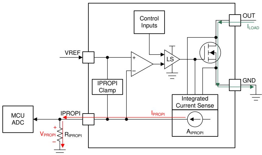
The IPROPI pin outputs an analog current proportional to the current flowing through the low-side power MOSFETs in the H-bridge scaled by $\mathsf { A } _ { | \mathsf { P R O P l } | } .$ . The IPROPI output current can be calculated by Equation 1. The $\mathsf { I } _ { \mathsf { L S x } }$ in Equation 1 is only valid when the current flows from drain to source in the low-side MOSFET. If when current flows from source to drain, the value of $\mathsf { I } _ { \mathsf { L S x } }$ for that channel is zero. For instance, if the bridge is in the brake, slow-decay state, then the current out of IPROPI is only proportional to the current in one of the low-side MOSFETs.
$$
I _ {P R O P I} (\mu A) = (I _ {L S 1} + I _ {L S 2}) (A) \times A _ {I P R O P I} (\mu A / A)\tag{1}
$$
The current is measured by an internal current mirror architecture that removes the needs for an external power sense resistor. Additionally, the current mirror architecture allows for the motor winding current to be sensed in both the drive and brake low-side slow-decay periods allowing for continuous current monitoring in typical bidirectional brushed DC motor applications. In coast mode, the current is freewheeling and cannot be sensed because it flow from source to drain. However, the current can be sampled by briefly reenabling the driver in either drive or slow-decay modes and measuring the current before switching back to coast mode again. In the case of independent PWM mode and both low-side MOSFETs are carrying current, the IPROPI output will be the sum of the two low-side MOSFET currents.
The IPROPI pin should be connected to an external resistor $\scriptstyle \left( { \mathsf { R } } _ { | { \mathsf { P R O P l } } } \right)$ to ground in order to generate a proportional voltage $( \mathsf { V } _ { \mathsf { I P R O P l } } )$ on the IPROPI pin with the $\mathsf { I } _ { | \mathsf { P R O P } | }$ analog current output. This allows for the load current to be measured as the voltage drop across the RIPROPI resistor with a standard analog to digital converter (ADC). The $\mathsf { R } _ { | \mathsf { P R O P l } }$ resistor can be sized based on the expected load current in the application so that the full range of the controller ADC is utilized. Additionally, the DRV887x devices implements an internal IPROPI voltage clamp circuit to limit $\mathsf { V } _ { | \mathsf { P R O P } | }$ with respect to $V _ { \mathsf { V R E F } }$ on the VREF pin and protect the external ADC in case of output overcurrent or unexpected high current events.
The corresponding IPROPI voltage to the output current can be calculated by Equation 2.
$$
V _ {I P R O P I} (V) = I _ {P R O P I} (A) \times R _ {I P R O P I}\tag{Ω}
$$
(2)
Copyright © 2017, Texas Instruments Incorporated
Figure 11. Integrated Current Sensing
The IPROPI output bandwidth is limited by the sense delay time $( \tt t _ { D E L A Y } )$ of the DRV887x internal current sensing circuit. This time is the delay from the low-side MOSFET enable command to the IPROPI output being ready. If the device is alternating between drive and slow-decay (brake) in an H-bridge PWM pattern then the low-side MOSFET sensing the current is continuously on and the sense delay time has no impact to the IPROPI output.
7.3.3.2 Current Regulation
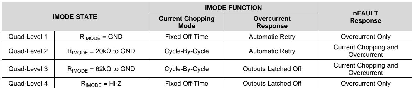
The DRV887x family of devices integrate current regulation using either a fixed off-time or cycle-by-cycle PWM current chopping scheme. The current chopping scheme is selectable through the IMODE quad-level input. This allows the devices to limit the output current in case of motor stall, high torque, or other high current load events.
The IMODE level can be set by leaving the pin floating (Hi-Z), connecting the pin to GND, or connecting a resistor between IMODE and GND. The IMODE pin state is latched when the device is enabled through the nSLEEP pin. The IMODE state can be changed by taking the nSLEEP pin logic low, waiting the $\mathfrak { t } _ { \mathtt { S L E E P } }$ time, changing the IMODE pin input, and then enabling the device by taking the nSLEEP pin back logic high. The IMODE input is also used to select the device response to an overcurrent event. See more details in the Protection Circuits section.
The internal current regulation can be disabled by tying IPROPI to GND and setting the VREF pin voltage greater than GND (if current feedback is not required) or if current feedback is required, setting $V _ { \mathsf { V R E F } }$ and $\mathsf { R } _ { | \mathsf { P R O P l } | }$ such that VIPROPI never reaches the $\mathsf { V } _ { \mathsf { V R E F } }$ threshold. In independent half-bridge control mode $( P M O D E = H i - Z )$ , the internal current regulation is automatically disabled since the outputs are operating independently and the current sense and regulation is shared between half-bridges.
Table 6. IMODE Functions
| IMODE STATE | IMODE FUNCTION | nFAULT Response | ||
| Current Chopping Mode | Overcurrent Response | |||
| Quad-Level 1 | $R_{IMODE} = GND$ | Fixed Off-Time | Automatic Retry | Overcurrent Only |
| Quad-Level 2 | $R_{IMODE} = 20k\Omega \text{ to GND}$ | Cycle-By-Cycle | Automatic Retry | Current Chopping and Overcurrent |
| Quad-Level 3 | $R_{IMODE} = 62k\Omega \text{ to GND}$ | Cycle-By-Cycle | Outputs Latched Off | Current Chopping and Overcurrent |
| Quad-Level 4 | $R_{IMODE} = Hi-Z$ | Fixed Off-Time | Outputs Latched Off | Overcurrent Only |
The current chopping threshold $( \mathsf { I } _ { \mathsf { T R I P } } )$ is set through a combination of the VREF voltage $( \mathsf { V } _ { \mathsf { V R E F } } )$ and IPROPI output resistor $( \mathsf { R } _ { | \mathsf { P R O P l } | } )$ . This is done by comparing the voltage drop across the external $\mathsf { R } _ { | \mathsf { P R O P l } }$ resistor to $\mathsf { V } _ { \mathsf { V R E F } }$ with an internal comparator.
$$
I _ {T R I P} (A) \times A _ {I P R O P I} (\mu A / A) = V _ {V R E F} (V) / R _ {I P R O P I} (\Omega)\tag{3}
$$
For example, if $\mathsf { V } _ { \mathsf { V R E F } } = 2 . 5 ~ \mathsf { V } , ~ \mathsf { R } _ { \mathsf { I P R O P } | } = 1 5 0 0 ~ \Omega$ , and $\mathsf { A } _ { | \mathsf { P R O P } | } = 1 0 0 0 ~ \mu \mathsf { A } / \mathsf { A }$ , then $\mathsf { I } _ { \mathsf { T R I P } }$ will be approximately 1.67 $\mathsf { A } .$
When the $\mathsf { I } _ { \mathsf { T R I P } }$ threshold is exceeded, the outputs will enter a current chopping mode according to the IMODE setting. The $\mathsf { I } _ { \mathsf { T R I P } }$ comparator has both a blanking time $( t _ { \mathsf { B L K } } )$ and a deglitch time $( \mathtt { t } _ { \mathtt { D E G } } )$ . The internal blanking time helps to prevent voltage and current transients during output switching from effecting the current regulation. These transients may be caused by a capacitor inside the motor or on the connections to the motor terminals. The internal deglitch time ensures that transient conditions do not prematurely trigger the current regulation. In certain cases where the transient conditions are longer than the deglitch time, placing a $1 0 - n F$ capacitor on the IPROPI pin, close to the DRV887x, will help filter the transients on IPROPI output so current regulation does not prematurely trigger. The capacitor value can be adjusted as needed, however large capacitor values may slow down the response time of the current regulation circuitry.
The $\mathsf { A } _ { \mathsf { E R R } }$ parameter in the Electrical Characteristics table is the error associated with the $\mathsf { A } _ { | \mathsf { P R O P l } }$ gain. It indicates the combined effect of offset error added to the $\mathsf { I } _ { \mathsf { O U T } }$ current and gain error.
7.3.3.2.1 Fixed Off-Time Current Chopping
In the fixed off-time mode, the H-bridge enters a brake/low-side slow decay state (both low-side MOSFETs ON) for $\boldsymbol { \mathrm { t } } _ { \mathsf { O F F } }$ duration after $\mathsf { I } _ { \mathsf { O U T } }$ exceeds $\mathsf { I } _ { \mathsf { T R I P } } ,$ . After $\boldsymbol { \mathrm { t } } _ { \mathsf { O F F } }$ the outputs are re-enabled according to the control inputs unless $\mathsf { I } _ { \mathsf { O U T } }$ is still greater than $\mathsf { I } _ { \mathsf { T R I P } }$ . If $\mathsf { I } _ { \mathsf { O U T } }$ is still greater than ${ \mathsf { I } } _ { { \mathsf { T R I P } } } ,$ the H-bridge will enter another period of brake/low-side slow decay for t . If the state of the EN/IN1 or PH/IN2 control pin inputs changes during the t time, the remainder of the $\mathsf { t } _ { \mathsf { O F F } }$ time is ignored, and the outputs will again follow the inputs.
The fixed off-time mode allows for a simple current chopping scheme without involvement from the external controller. This is shown in Figure 12. Fixed off-time mode will support 100% duty cycle current regulation since the H-bridge automatically enables after the $\mathsf { t } _ { \mathsf { O F F } }$ period and does not require a new control input edge on the EN/IN1 or PH/IN2 pins to reset the outputs.
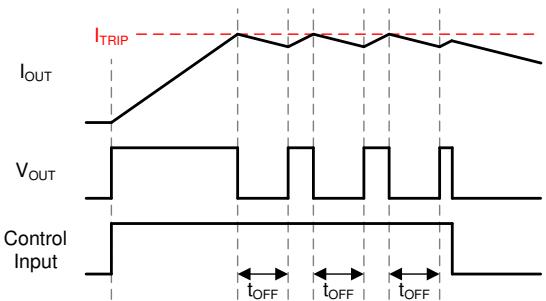
Figure 12. Off-Time Current-Regulation
7.3.3.2.2 Cycle-By-Cycle Current Chopping
In cycle-by-cycle mode, the H-bridge enters a brake, low-side slow decay state (both low-side MOSFETs ON) after $\mathsf { I } _ { \mathsf { O U T } }$ exceeds $\mathsf { I } _ { \mathsf { T R I P } }$ until the next control input edge on the EN/IN1 or PH/IN2 pins. This allows for additional control of the current chopping scheme by the external controller. This is shown in Figure 13. Cycle-by-cycle mode will not support 100% duty cycle current regulation as a new control input edge is required to reset the outputs after the brake, low-side slow decay state has been entered.
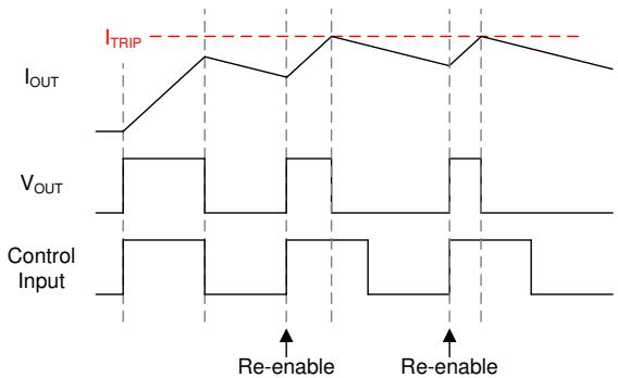
Figure 13. Cycle-By-Cycle Current Regulation
In cycle-by-cycle mode, the device will also indicates whenever the H-bridge has entered internal current chopping by pulling the nFAULT pin low. This can be used to determine when the device outputs will differ from the control inputs or the load has reached the $\mathsf { I } _ { \mathsf { T R I P } }$ threshold. This is shown in Figure 14. nFAULT will be released whenever the next control input edge is received by the device and the outputs are reset.
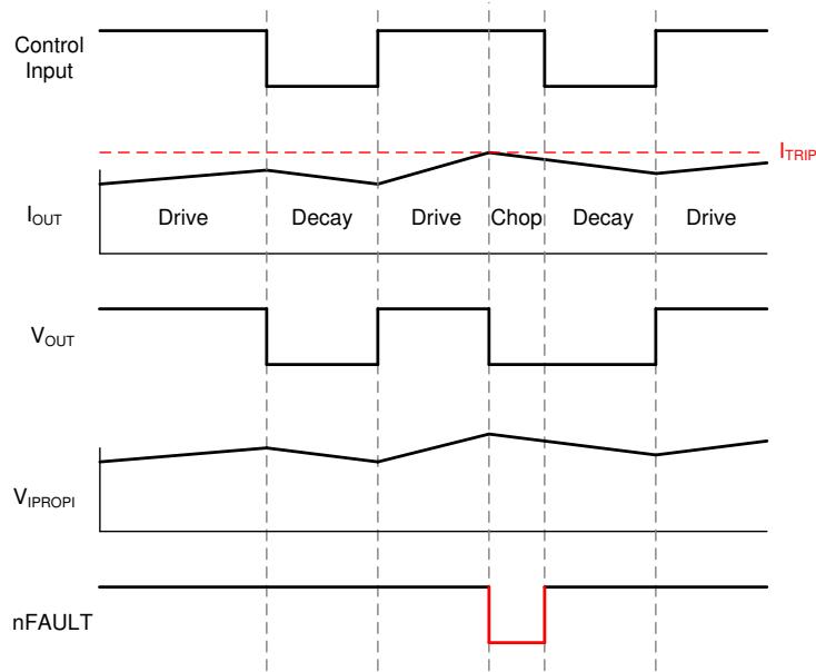
Figure 14. Cycle-By-Cycle Current Regulation
No device functionality is affected when the nFAULT pin is pulled low for the current chopping indicator. The nFAULT pin is only used as an indicator and the device will continue normal operation. To distinguish from a device fault (outlined in the Protection Circuits section) from the current chopping indicator, the nFAULT pin can be compared with the control inputs. The current chopping indicator can only assert when the control inputs are commanding a forward or reverse drive state (Figure 10). If the nFAULT pin is pulled low and the control inputs are commanding the high-Z or slow-decay states, then a device fault has occurred.
7.3.4 Protection Circuits
The DRV887x family of devices are fully protected against supply undervoltage, charge pump undervoltage, output overcurrent, and device overtemperature events.
7.3.4.1 VM Supply Undervoltage Lockout (UVLO)
If at any time the supply voltage on the VM pin falls below the undervoltage lockout threshold voltage $( \mathsf { V } _ { \mathsf { U V L O } } )$ , all MOSFETs in the H-bridge will be disabled and the nFAULT pin driven low. The charge pump is disabled in this condition. Normal operation will resume when the undervoltage condition is removed and VM rises above the $\mathsf { V } _ { \mathsf { U V L O } }$ threshold.
7.3.4.2 VCP Charge Pump Undervoltage Lockout (CPUV)
If at any time the charge pump voltage on the VCP pin falls below the undervoltage lockout threshold voltage $( \mathsf { V } _ { \mathsf { C P U V } } )$ , all MOSFETs in the H-bridge will be disabled and the nFAULT pin driven low. Normal operation will resume when the undervoltage condition is removed and VCP rises above the $\mathsf { V } _ { \mathsf { C P U V } }$ threshold.
7.3.4.3 OUTx Overcurrent Protection (OCP)
An analog current limit circuit on each MOSFET limits the peak current out of the device even in hard short circuit events.
If the output current exceeds the overcurrent threshold, I , for longer than $\mathsf { t _ { O C P } } ,$ , all MOSFETs in the H-bridge will be disabled and the nFAULT pin driven low. The overcurrent response can be configured through the IMODE pin as shown in Table 6.
In automatic retry mode, the MOSFETs will be disabled and nFAULT pin driven low for a duration of $\mathsf { t } _ { \mathsf { R E T R Y } } .$ . After t , the MOSFETs are re-enabled according to the state of the EN/IN1 and PH/IN2 pins. If the overcurrent condition is still present, the cycle repeats; otherwise normal device operation resumes.
In latched off mode, the MOSFETs will remain disabled and nFAULT pin driven low until the device is reset through either the nSLEEP pin or by removing the VM power supply.
In Independent Half-Bridge Control Mode (PMODE = Hi-Z), the OCP behavior is slightly modified. If an overcurrent event is detected, only the corresponding half-bridge will be disabled and the nFAULT pin driven low. The other half-bridge will continue normal operation. This allows for the device to manage independent fault events when driving independent loads. If an overcurrent event is detected in both half-bridges, both half-bridges will be disabled and the nFAULT pin driven low. In automatic retry mode, both half-bridges share the same overcurrent retry timer. If an overcurrent event occurs first in one half-bridge and then later in the secondary halfbridge, but before $\tt t _ { R E T R Y }$ has expired, the retry timer for the first half-bridge will be reset to $\tt t _ { R E T R Y }$ and both halfbridges will enable again after the retry timer expires.
7.3.4.4 Thermal Shutdown (TSD)
If the die temperature exceeds the overtemperature limit ${ \sf T } _ { \sf \sf T S D } .$ , all MOSFET in the H-bridge will be disabled and the nFAULT pin driven low. Normal operation will resume when the overtemperature condition is removed and the die temperature drops below the $T _ { \mathsf { T S D } }$ threshold.
7.3.4.5 Fault Condition Summary
Table 7. Fault Condition Summary
| FAULT | CONDITION | REPORT | H-BRIDGE | RECOVERY |
| ITRIP Indicator | CBC Mode & IOUT > ITRIP | nFAULT | Active Low-Side Slow Decay | Control Input Edge |
| VM Undervoltage Lockout (UVLO) | VM < VUVLO | nFAULT | Disabled | VM > VUVLO |
| VCP Undervoltage Lockout (CPUV) | VCP < VCPUV | nFAULT | Disabled | VCP > VCPUV |
| Overcurrent (OCP) | IOUT > IOCP | nFAULT | Disabled | tRETRY or Reset (Set by IMODE) |
| Thermal Shutdown (TSD) | TJ > TTSD | nFAULT | Disabled | TJ < TTSD - THYS |
7.3.5 Pin Diagrams
7.3.5.1 Logic-Level Inputs
Figure 15 shows the input structure for the logic-level input pins EN/IN1, PH/IN2, and nSLEEP.
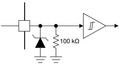
Figure 15. Logic-Level Input
7.3.5.2 Tri-Level Inputs
Figure 16 shows the input structure for the tri-level input pin PMODE.
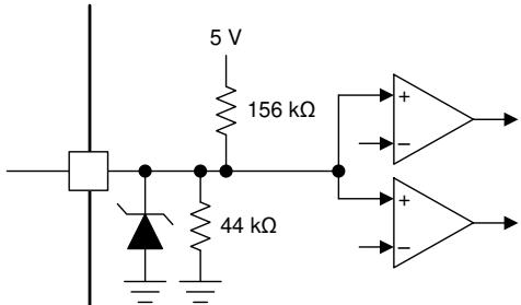
Figure 16. PMODE Tri-Level Input
7.3.5.3 Quad-Level Inputs
Figure 17 shows the input structure for the quad-level input pin IMODE.
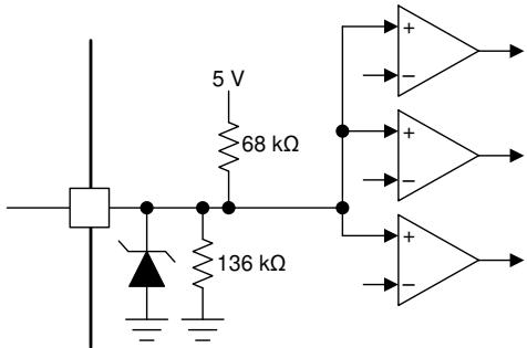
Figure 17. Quad-Level Input
7.4 Device Functional Modes
The DRV887x family of devices have several different modes of operation depending on the system inputs.
7.4.1 Active Mode
After the supply voltage on the VM pin has crossed the undervoltage threshold $\mathsf { V } _ { \mathsf { U V L O } } ,$ the nSLEEP pin is logic high, and tWAKE has elapsed, the device enters its active mode. In this mode, the H-bridge, charge pump, and internal logic are active and the device is ready to receive inputs. The input control mode (PMODE) and current control modes (IMODE) will be latched when the device enters active mode.
Device Functional Modes (continued)
7.4.2 Low-Power Sleep Mode
The DRV887x family of devices support a low power mode to reduce current consumption from the VM pin when the driver is not active. This mode is entered by setting the nSLEEP pin logic low and waiting for t to elapse. In sleep mode, the H-bridge, charge pump, internal 5-V regulator, and internal logic are disabled. The device relies on a weak pulldown to ensure all of the internal MOSFETs remain disabled. The device will not respond to any inputs besides nSLEEP while in low-power sleep mode.
7.4.3 Fault Mode
The DRV887x family of devices enter a fault mode when a fault is encountered. This is utilized to protect the device and the output load. The device behavior in the fault mode is described in Table 7 and depends on the fault condition. The device will leave the fault mode and re-enter the active mode when the recovery condition is met.
8 Application and Implementation
NOTE
Information in the following applications sections is not part of the TI component specification, and TI does not warrant its accuracy or completeness. TI’s customers are responsible for determining suitability of components for their purposes. Customers should validate and test their design implementation to confirm system functionality.
8.1 Application Information
The DRV887x family of devices can be used in a variety of applications that require either a half-bridge or Hbridge power stage configuration. Common application examples include brushed DC motors, solenoids, and actuators. The device can also be utilized to drive many common passive loads such as LEDs, resistive elements, relays, etc. The application examples below will highlight how to use the device in bidirectional current control applications requiring an H-bridge driver and dual unidirectional current control applications requiring two half-bridge drivers.
8.2 Typical Application
8.2.1 Primary Application
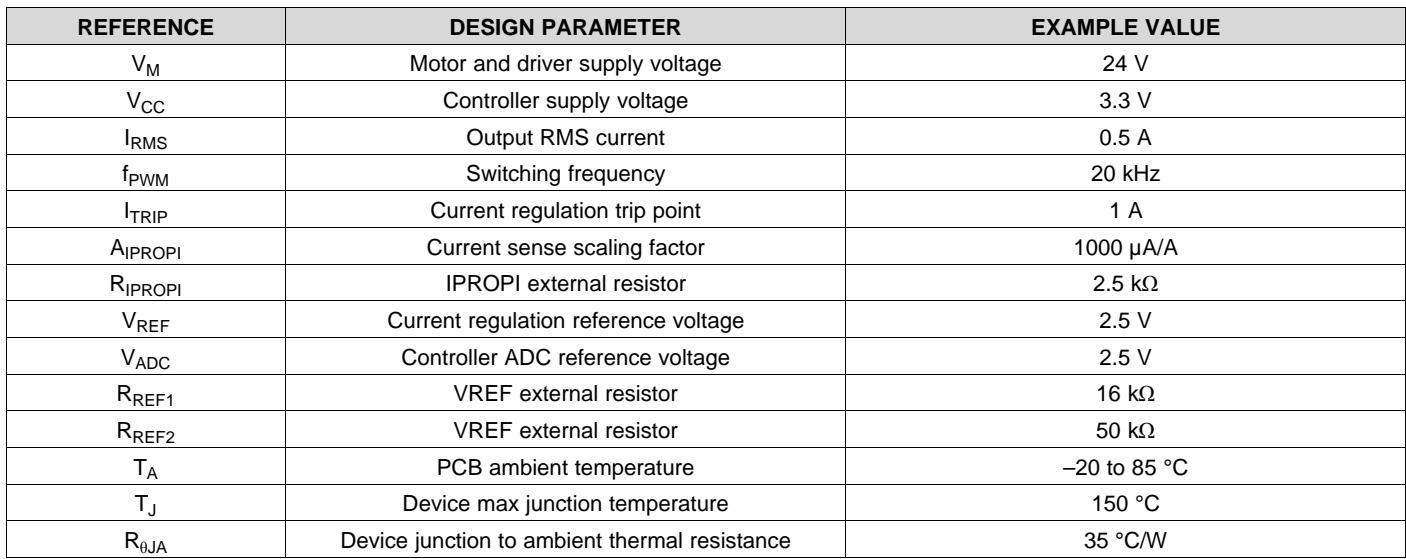
In the primary application example, the device is configured to drive a bidirectional current through an external load (such as a brushed DC motor) using an H-bridge configuration. The H-bridge polarity and duty cycle are controlled with a PWM and IO resource from the external controller to the EN/IN1 and PH/IN2 pins. The device is configured for the PH/EN control mode by tying the PMODE pin to GND. The current limit threshold $( \mathsf { I } _ { \mathsf { T R I P } } )$ is generated with an external resistor divider from the control logic supply voltage $( \mathsf { V } _ { \mathsf { C C } } )$ . The device is configured for the fixed off-time current regulation scheme by tying the IMODE pin to GND. The load current is monitored with an ADC from the controller to detect the voltage across $\mathsf { R } _ { | \mathsf { P R O P l } | }$

Figure 18. Typical Application Schematic
Typical Application (continued)
8.2.1.1 Design Requirements
Table 8. Design Parameters
| REFERENCE | DESIGN PARAMETER | EXAMPLE VALUE |
| $V_M$ | Motor and driver supply voltage | 24 V |
| $V_{CC}$ | Controller supply voltage | 3.3 V |
| $I_{RMS}$ | Output RMS current | 0.5 A |
| $f_{PWM}$ | Switching frequency | 20 kHz |
| $I_{TRIP}$ | Current regulation trip point | 1 A |
| $A_{IPROPI}$ | Current sense scaling factor | 1000 μA/A |
| $R_{IPROPI}$ | IPROPI external resistor | 2.5 kΩ |
| $V_{REF}$ | Current regulation reference voltage | 2.5 V |
| $V_{ADC}$ | Controller ADC reference voltage | 2.5 V |
| $R_{REF1}$ | VREF external resistor | 16 kΩ |
| $R_{REF2}$ | VREF external resistor | 50 kΩ |
| $T_A$ | PCB ambient temperature | -20 to 85 °C |
| $T_J$ | Device max junction temperature | 150 °C |
| $R_{\theta JA}$ | Device junction to ambient thermal resistance | 35 °C/W |
8.2.1.2 Detailed Design Procedure
8.2.1.2.1 Current Sense and Regulation
The DRV887x family of devices provide integrated regulation and sensing out the output current.
The current sense feedback is configured by scaling the $\mathsf { R } _ { | \mathsf { P R O P } | }$ resistor to properly sense the scaled down output current from IPROPI within the dynamic voltage range of the controller ADC. An example of this is shown.
$$
R _ {I P R O P I} < = V _ {A D C} / \left(I _ {T R I P} \times A _ {I P R O P I}\right)\tag{4}
$$
$$
R _ {I P R O P I} = 2. 5 \mathrm{k} \Omega < = 2. 5 \mathrm{V} / (1 \mathrm{A} \times 1 0 0 0 \mu \mathrm{A} / \mathrm{A})\tag{5}
$$
If $\mathsf { V } _ { \mathsf { A D C } } = 2 . 5 ~ \mathsf { V } , ~ \mathsf { I } _ { \mathsf { T R I P } } = 1 ~ \mathsf { A }$ , and $\mathsf { A } _ { | \mathsf { P R O P } | } = 1 0 0 0 \ \mu \mathsf { A } / \mathsf { A }$ then to maximize the dynamic IPROPI voltage range an $\mathsf { R } _ { | \mathsf { P R O P l } }$ of approximately 2.5 kΩ should be selected.
The accuracy tolerance of $\mathsf { R } _ { | \mathsf { P R O P l } }$ can be selected based on the application requirements. 10%, 5%, 1%, 0.1% are all valid tolerance values. The typical recommendation is 1% for best tradeoff between performance and cost.
The output current regulation trip point (I ) is configured with a combination of $V _ { \mathsf { R E F } }$ and $\mathsf { R } _ { | \mathsf { P R O P l } | }$ . Since RIPROPI was previously calculated and $\mathsf { A } _ { | \mathsf { P R O P l } | }$ is a constant, all the remains is to calculate $V _ { \mathsf { R E F } }$
$$
V _ {R E F} = R _ {I P R O P I} \times \left(I _ {T R I P} \times A _ {I P R O P I}\right)\tag{6}
$$
$$
V _ {R E F} = 2. 5 \mathrm{V} = 2. 5 \mathrm{k} \Omega \times (1 \mathrm{A} \times 1 0 0 0 \mu \mathrm{A} / \mathrm{A})\tag{7}
$$
$$
\text { If } R _ {\mathrm{IPROPI}} = 2. 5 \mathrm{k} \Omega , I _ {\mathrm{TRIP}} = 1 \mathrm{A}, \text { and } A _ {\mathrm{IPROPI}} = 1 0 0 0 \mu \mathrm{A/A} \text { then } V _ {\mathrm{REF}} \text { should be set to } 2. 5 \mathrm{V}.
$$
$V _ { \mathsf { R E F } }$ can be generated with a simple resistor divider $( R _ { R E F 1 }$ and $\mathsf { R } _ { \mathsf { R E F 2 } } )$ from the controller supply voltage. The resistor sizing can be achieved by selecting a value for $\mathsf { R } _ { \mathsf { R E F 1 } }$ and calculating the required value for ${ \mathsf { R } } _ { \mathsf { R E F 2 } }$
8.2.1.2.2 Power Dissipation and Output Current Capability
The output current and power dissipation capabilities of the device are heavily dependent on the PCB design and external system conditions. This section provides some guidelines for calculating these values.
Total power dissipation for the device is composed of three main components. These are the quiescent supply current dissipation, the power MOSFET switching losses. and the power MOSFET ${ \mathsf { R } } _ { \mathsf { D S } ( \mathsf { o n } ) }$ (conduction) losses. While other factors may contribute additional power losses, these other items are typically insignificant compared to the three main items.
$$
P _ {T O T} = P _ {V M} + P _ {S W} + P _ {R D S}\tag{8}
$$
$\mathsf { P } _ { \mathsf { V M } }$ can be calculated from the nominal supply voltage $( \mathsf { V } _ { \mathsf { M } } )$ and the $\mathsf { I } _ { \mathsf { V M } }$ active mode current specification.
$$
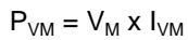
P _ {V M} = V _ {M} \times I _ {V M}\tag{9}
$$
$$
P _ {V M} = 0. 0 9 6 \mathrm{W} = 2 4 \mathrm{V} \times 4 \mathrm{mA}\tag{10}
$$
PSW can be calculated from the nominal supply voltage $( \mathsf { V } _ { \mathsf { M } } )$ , average output current (IRMS), switching frequency (fPWM) and the device output rise $( \mathfrak { t } _ { \mathsf { R } 1 \mathsf { S } \mathsf { E } } )$ and fall $( \tt t _ { F A L L } )$ time specifications.
$$
P _ {S W} = P _ {S W _ R I S E} + P _ {S W _ F A L L}\tag{11}
$$
$$
P _ {S W _ R I S E} = 0. 5 \times V _ {M} \times I _ {R M S} \times t _ {R I S E} \times f _ {P W M}\tag{12}
$$
$$
P _ {S W _ F A L L} = 0. 5 \times V _ {M} \times I _ {R M S} \times t _ {F A L L} \times f _ {P W M}\tag{13}
$$
$$
P _ {S W _ R I S E} = 0. 0 1 8 \mathrm{W} = 0. 5 \times 2 4 \mathrm{V} \times 0. 5 \mathrm{A} \times 1 5 0 \mathrm{ns} \times 2 0 \mathrm{kHz}\tag{14}
$$
$$
P _ {S W _ F A L L} = 0. 0 1 8 \mathrm{W} = 0. 5 \times 2 4 \mathrm{V} \times 0. 5 \mathrm{A} \times 1 5 0 \mathrm{ns} \times 2 0 \mathrm{kHz}\tag{15}
$$
$$
P _ {S W} = 0. 0 3 6 \mathrm{W} = 0. 0 1 8 \mathrm{W} + 0. 0 1 8 \mathrm{W}\tag{16}
$$
PRDS can be calculated from the device ${ \mathsf { R } } _ { \mathsf { D S } ( \mathsf { o n } ) }$ and average output current (IRMS)
$$
P _ {R D S} = I _ {R M S} ^ {2} \times (R _ {D S (O N) _ H S} + R _ {D S (O N) _ L S})\tag{17}
$$
It should be noted that ${ \mathsf { R } } _ { \mathsf { D S } ( \mathsf { O N } ) }$ has a strong correlation with the device temperature. A curve showing the normalized ${ \mathsf { R } } _ { \mathsf { D S } ( \mathsf { o n } ) }$ with temperature can be found in the Typical Characteristics curves. Assuming a device temperature of $8 5 ^ { \circ } C$ it can be expected that ${ \mathsf { R } } _ { \mathsf { D S } ( \mathsf { o n } ) }$ will see an increases of ~1.25 based on the normalized temperature data.
$$
P _ {R D S} = 0. 2 1 9 \mathrm{W} = (0. 5 \mathrm{A}) ^ {2} \times (3 5 0 \mathrm{m} \Omega \times 1. 2 5 + 3 5 0 \mathrm{m} \Omega \times 1. 2 5)\tag{18}
$$
By adding together the different power dissipation components it can be verified that the expected power dissipation and device junction temperature is within design targets.
$$
P _ {T O T} = P _ {V M} + P _ {S W} + P _ {R D S}\tag{19}
$$
$$
P _ {T O T} = 0. 3 5 1 \mathrm{W} = 0. 0 9 6 \mathrm{W} + 0. 0 3 6 \mathrm{W} + 0. 2 1 9 \mathrm{W}\tag{20}
$$
The device junction temperature can be calculated with the $\mathsf { P } _ { \mathsf { T O T } }$ , device ambient temperature $( \mathsf { T } _ { \mathsf { A } } )$ , and package thermal resistance $( \mathsf { R } _ { \mathsf { \theta J A } } )$ . The value for $\mathsf { R } _ { \mathsf { \theta J A } }$ is heavily dependent on the PCB design and copper heat sinking around the device.
$$
T _ {J} = (P _ {T O T} \times R _ {\theta J A}) + T _ {A}\tag{21}
$$
$$
T _ {J} = 9 7 ^ {\circ} \mathrm{C} = (0. 3 5 1 \mathrm{W} \times 3 5 ^ {\circ} \mathrm{C} / \mathrm{W}) + 8 5 ^ {\circ} \mathrm{C}\tag{22}
$$
It should be ensured that the device junction temperature is within the specified operating region. Other methods exist for verifying the device junction temperature depending on the measurements available.
Additional information on motor driver current ratings and power dissipation can be found in Thermal Performance and Related Documentation.
8.2.1.2.3 Thermal Performance
The datasheet-specified junction-to-ambient thermal resistance, $\mathsf { R } _ { \Theta \mathsf { J } \mathsf { A } } ,$ is primarily useful for comparing various drivers or approximating thermal performance. However, the actual system performance may be better or worse than this value depending on PCB stackup, routing, number of vias, and copper area around the thermal pad. The length of time the driver drives a particular current will also impact power dissipation and thermal performance. This section considers how to design for steady-state and transient thermal conditions.
The data in this section was simulated using the following criteria:
HTSSOP (PWP package)
• 2-layer PCB, standard FR4, 1-oz (35 mm copper thickness) or 2-oz copper thickness.
• Top layer: DRV887x HTSSOP package footprint and copper plane heatsink. Top layer copper area is varied in simulation.
Bottom layer: ground plane thermally connected through vias under the thermal pad for DRV887x. Bottom layer copper area varies with top copper area. Thermal vias are only present under the thermal pad (grid pattern with 1.2mm spacing).
• 4-layer PCB, standard FR4. Outer planes are 1-oz (35 mm copper thickness) or 2-oz copper thickness.
• Top layer: DRV887x HTSSOP package footprint and copper plane heatsink. Top layer copper area is varied in simulation. Inner planes were kept at 1-oz.
• Mid layer 1: GND plane thermally connected to DRV887x thermal pad through vias. The area of the ground plane is 74.2 mm x 74.2 mm.
• Mid layer 2: power plane, no thermal connection.
Bottom layer: signal layer with small copper pad underneath DRV887x and thermally connected through via stitching from the TOP and internal GND planes. Bottom layer thermal pad is the same size as the package (5 mm x 4.4 mm). Bottom pad size remains constant as top copper plane is varied. Thermal vias are only present under the thermal pad (grid pattern with 1.2mm spacing).
Figure 19 shows an example of the simulated board for the HTSSOP package. Table 9 shows the dimensions of the board that were varied for each simulation.
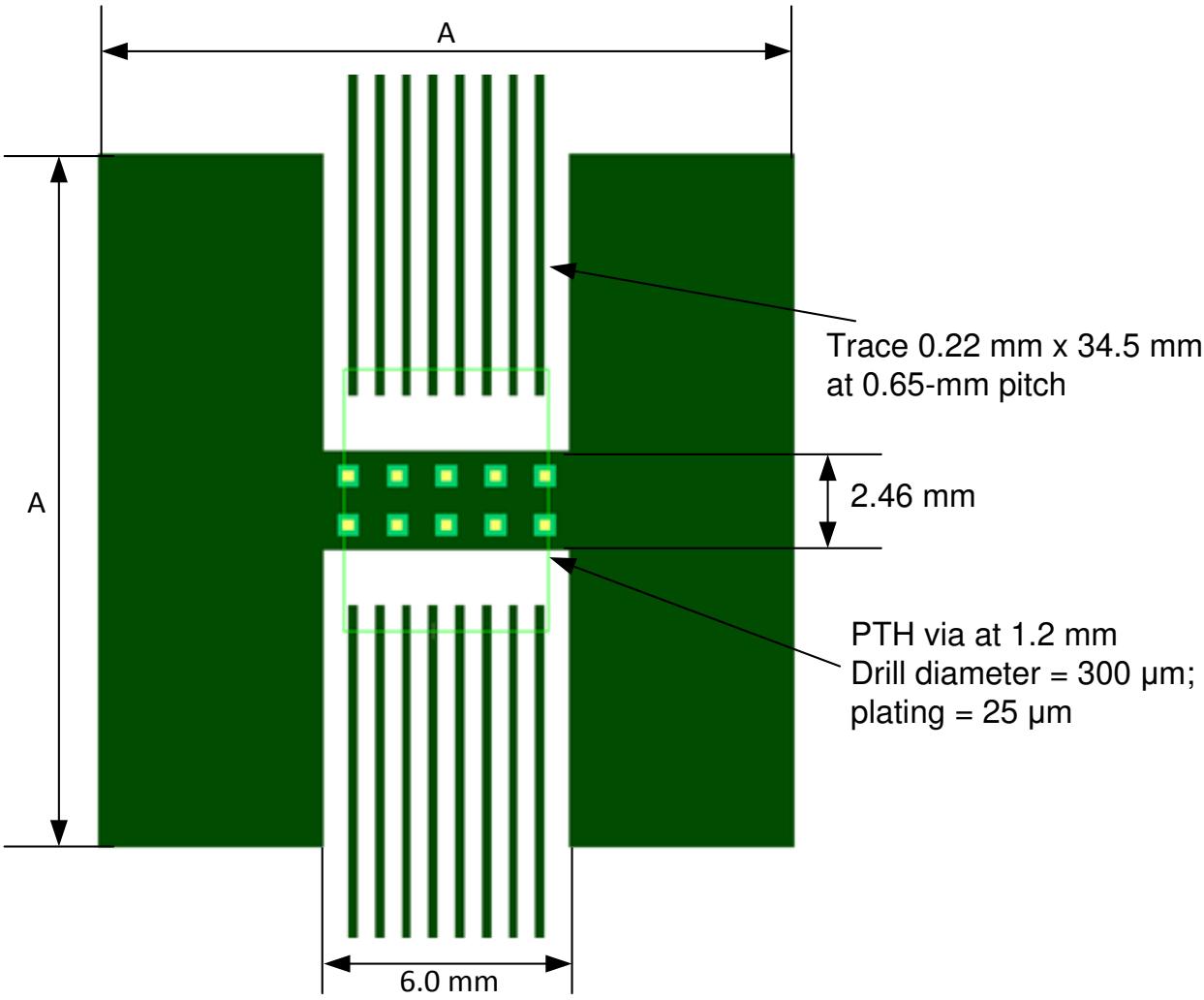
Figure 19. HTSSOP PCB model top layer
Table 9. Dimension A for 16-pin PWP package
| Cu area (mm2) | Dimension A (mm) |
| 2 | 17.0 |
| 4 | 22.8 |
| 8 | 31.0 |
| 16 | 42.8 |
VQFN (RGT package)
• 2-layer PCB, standard FR4, 1-oz (35 mm copper thickness) or 2-oz copper thickness.
• Top layer: DRV887x VQFN package footprint.
Bottom layer: ground plane thermally connected through vias under the thermal pad for DRV887x. Bottom layer copper area is varied in simulation. Thermal vias are only present under the thermal pad (grid
pattern with 1.2mm spacing).
• 4-layer PCB, standard FR4. Outer planes are 1-oz (35 mm copper thickness) or 2-oz copper thickness.
• Top layer: DRV887x VQFN package footprint. Inner planes were kept at 1-oz.
• Mid layer 1: GND plane thermally connected to DRV887x thermal pad through vias. The area of the ground plane is 74.2 mm x 74.2 mm.
• Mid layer 2: power plane, no thermal connection.
Bottom layer: signal layer with small copper pad underneath DRV887x and thermally connected through via stitching from the TOP and internal GND planes. Bottom layer thermal pad is the same size as the package (3 mm x 3 mm). Bottom pad size remains constant. Thermal vias are only present under the thermal pad (grid pattern with 1.2mm spacing).
Figure 20 shows an example of the simulated board. Table 10 shows the dimensions of the board that were varied for each simulation.

Figure 20. VQFN PCB model top layer
Table 10. Dimension A for 16-pin VQFN package
| Cu area (mm2) | Dimension A (mm) |
| 2 | 14.14 |
| 4 | 20.00 |
| 8 | 28.28 |
| 16 | 40.00 |
8.2.1.2.3.1 Steady-State Thermal Performance
"Steady-state" conditions assume that the motor driver operates with a constant RMS current over a long period of time. Figure 21, Figure 22, Figure 23, and Figure 24 show how $\mathsf { R } _ { \mathsf { \theta J A } }$ and $\Psi _ { \mathsf { J B } }$ (junction-to-board characterization parameter) change depending on copper area, copper thickness, and number of layers of the PCB for the HTSSOP package. More copper area, more layers, and thicker copper planes decrease $\mathsf { R } _ { \mathsf { \theta J A } }$ and $\Psi _ { \mathsf { J B } } ,$ which indicate better thermal performance from the PCB layout.

Figure 21. HTSSOP, 4-layer PCB junction-to-ambient thermal resistance vs copper area
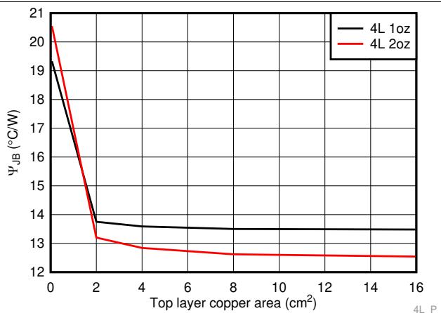
Figure 22. HTSSOP, 4-layer PCB junction-to-board characterization parameter vs copper area
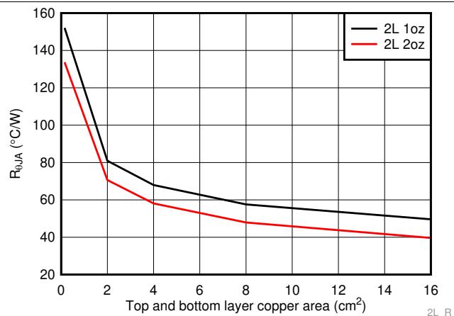
Figure 23. HTSSOP, 2-layer PCB junction-to-ambient thermal resistance vs copper area

Figure 24. HTSSOP, 2-layer PCB junction-to-board characterization parameter vs copper area
Figure 25 and Figure 26 show how $\mathsf { R } _ { \mathsf { \theta J A } }$ and $\Psi _ { \mathsf { J B } }$ vary with the bottom layer copper area for the VQFN package mounted on a 2-layer board. In the case of the 4-layer board, the top-layer copper area cannot be varied. Figure 29 and Figure 30 at 1000 s show the steady-state $\mathsf { R } _ { \mathsf { \theta J A } }$ of the 4-layer board.

Figure 25. VQFN, 2-layer PCB junction-to-ambient thermal resistance vs copper area

Figure 26. VQFN, 2-layer PCB junction-to-board characterization parameter vs copper area
8.2.1.2.3.2 Transient Thermal Performance
The motor driver may experience different transient driving conditions that cause large currents to flow for a short duration of time. These may include
• Motor start-up when the rotor is not yet spinning at full speed.
• Fault conditions when there is a supply or ground short to one of the motor outputs, and the device goes into and out of overcurrent protection.
• Briefly energizing a motor or solenoid for a limited time, then de-energizing.
For these transient cases, the duration of drive time is another factor that impacts thermal performance. In transient cases, the thermal impedance parameter $Z _ { \tt \theta J A }$ denotes the junction-to-ambient thermal performance. Figure 27 and Figure 28 show the simulated thermal impedances for 1-oz and 2-oz copper layouts for the HTSSOP package. These graphs indicate better thermal performance with short current pulses. For short periods of drive time, the device die size and package dominates the thermal performance. For longer drive pulses, board layout has a more significant impact on thermal performance. Both graphs show the curves for thermal impedance split due to number of layers and copper area as the duration of the drive pulse duration increases. Long pulses can be considered steady-state performance.
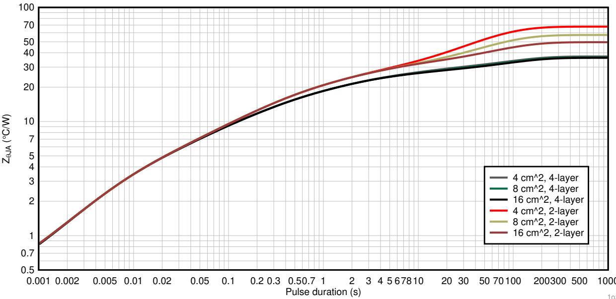
Figure 27. HTSSOP package junction-to-ambient thermal impedance for 1-oz copper layouts
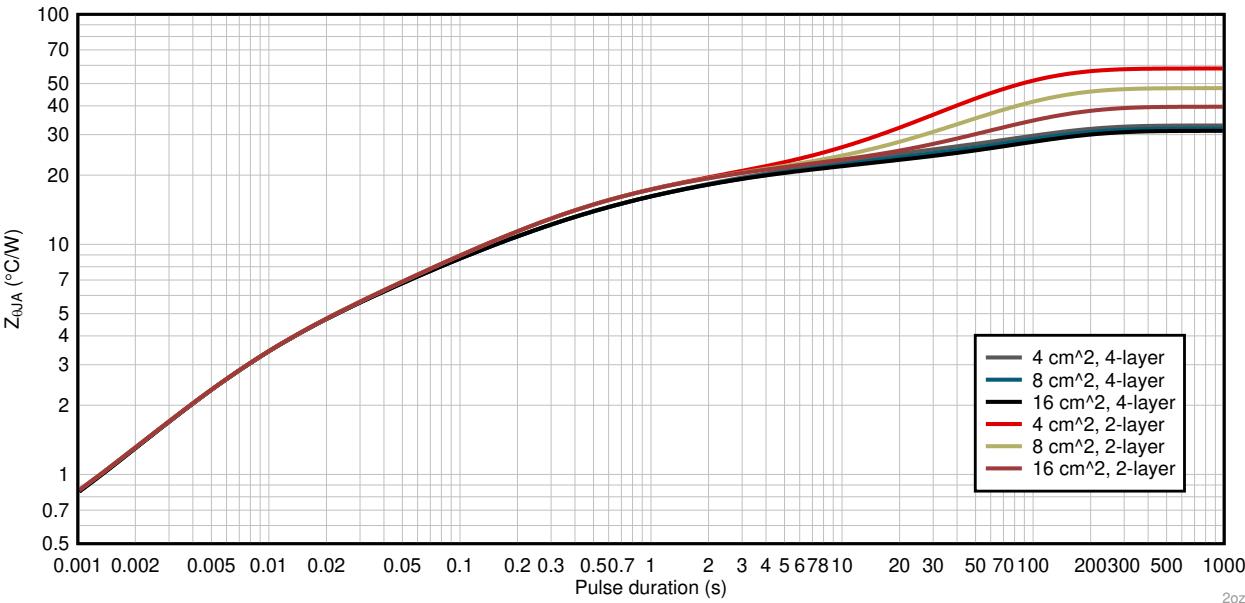
Figure 28. HTSSOP package Junction-to-ambient thermal impedance for 2-oz copper layouts
Figure 29 and Figure 30 show the transient thermal performance for the VQFN package with 2-layer and 4-layer PCB layouts. For this simulation, only the bottom layer was varied for the 2-layer case because the pins of the VQFN package constrain the copper area under the chip on the top layer.
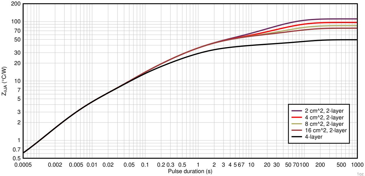
Figure 29. VQFN package junction-to-ambient thermal impedance for 1-oz copper layouts
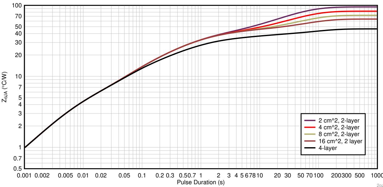
Figure 30. VQFN package Junction-to-ambient thermal impedance for 2-oz copper layouts
8.2.1.3 Application Curves
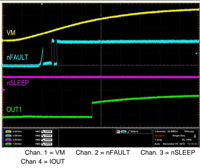
Figure 31. Device Power-up with Supply Voltage (VM) Ramp

Figure 32. Device Power-up with nSLEEP
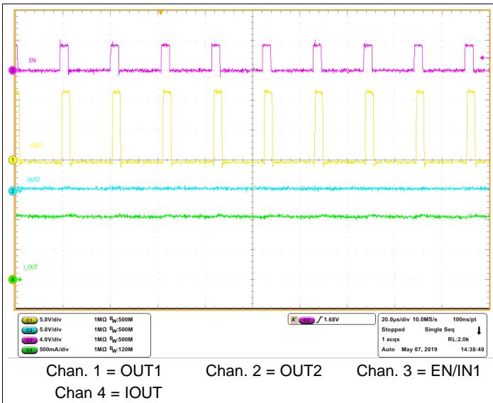
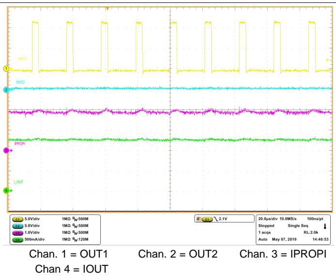
Figure 34. Driver PWM Operation With Current Feedback
Figure 33. Driver PWM Operation (PH/EN)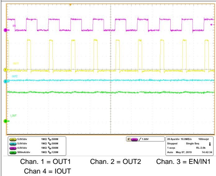
Figure 35. Driver PWM Operation With Current Chopping

Figure 36. Driver Full On Operation With Current Chopping
8.2.2 Alternative Application
In the alternative application example, the device is configured to drive a unidirectional current through two external loads (such as two brushed DC motors) using a dual half-bridge configuration. The duty cycle of each half-bridge is controlled with a PWM resource from the external controller to the EN/IN1 and PH/IN2 pins. The device is configured for the independent half-bridge control mode by leaving the PMODE pin floating. Since the current regulation scheme is disabled in the independent half-bridge control mode, the VREF pin is tied to VCC. The combined load current is monitored with an ADC from the controller to detect the voltage across RIPROPI.
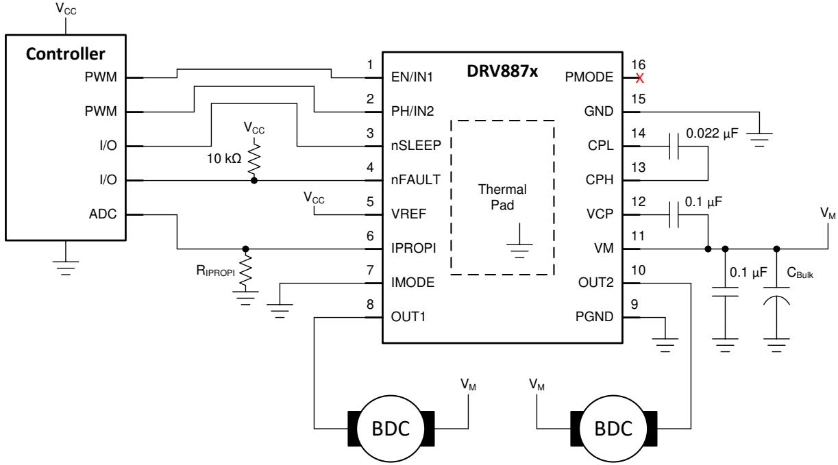
Figure 37. Typical Application Schematic
8.2.2.1 Design Requirements
Table 11. Design Parameters
| REFERENCE | DESIGN PARAMETER | EXAMPLE VALUE |
| $V_M$ | Motor and driver supply voltage | 24 V |
| $V_{CC}$ | Controller supply voltage | 3.3 V |
| $I_{RMS1}$ | Output 1 RMS current | 0.5 A |
| $I_{PEAK1}$ | Output 1 peak current | 1 A |
| $I_{RMS2}$ | Output 2 RMS current | 0.25 A |
| $I_{PEAK2}$ | Output 2 peak current | 0.5 A |
| $f_{PWM}$ | Switching frequency | 20 kHz |
| $A_{IPROPI}$ | Current sense scaling factor | 1000 μA/A |
| $R_{IPROPI}$ | IPROPI external resistor | 2.2 kΩ |
| $V_{ADC}$ | Controller ADC reference voltage | 3.3 V |
| $T_A$ | PCB ambient temperature | -20 to 85 °C |
| $T_J$ | Device max junction temperature | 150 °C |
| $R_{\theta JA}$ | Device junction to ambient thermal resistance | 35 °C/W |
8.2.2.2 Detailed Design Procedure
Refer to the Primary Application Detailed Design Procedure section for a detailed design procedure example. The majority of the design concepts apply to the alternative application example. A few changes to the procedure are outlined below.
8.2.2.2.1 Current Sense and Regulation
In the alternative application for two half-bridge loads, the IPROPI output will be the combination of the two outputs currents. The current sense feedback resistor $\mathsf { R } _ { | \mathsf { P R O P } | }$ should be scaled appropriately to stay within the dynamic voltage range of the controller ADC. An example of this is shown
$$
R _ {I P R O P I} < = V _ {A D C} / \left(\left(I _ {P E A K 1} + I _ {P E A K 2}\right) \times A _ {I P R O P I}\right)\tag{23}
$$
$$
R _ {I P R O P I} = 2. 2 \mathrm{k} \Omega < = 3. 3 \mathrm{V} / ((1 \mathrm{A} + 0. 5 \mathrm{A}) \times 1 0 0 0 \mu \mathrm{A} / \mathrm{A})\tag{24}
$$
If ${ \mathsf { V } } _ { \mathsf { A D C } } = 3 . 3 { \mathsf { V } } ,$ , IPEAK1 = 1 A, $\mathsf { I } _ { \mathsf { P E A K 2 } } = 0 . 5 \mathsf { A } ,$ and $\mathsf { A } _ { | \mathsf { P R O P } | } = 1 0 0 0 \ \mu \mathsf { A } / \mathsf { A } 4 5 5$ µA/A then to maximize the dynamic IPROPI voltage range an RIPROPI of approximately 2.2 kΩ should be selected.
The accuracy tolerance of $\mathsf { R } _ { | \mathsf { P R O P l } }$ can be selected based on the application requirements. 10%, 5%, 1%, 0.1% are all valid tolerance values. The typical recommendation is 1% for best tradeoff between performance and cost.
In independent half-bridge mode, the internal current regulation of the device is disabled. $V _ { \mathsf { R E F } }$ can be set directly to the supply reference for the controller ADC.
8.2.2.3 Application Curves
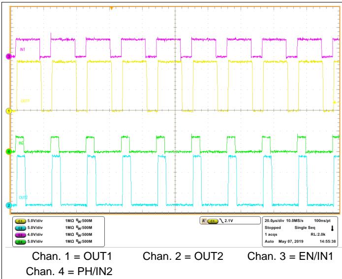
Figure 38. Independent Half-Bridge PWM Operation

Figure 39. Independent Half-Bridge PWM Operation
9 Power Supply Recommendations
9.1 Bulk Capacitance
Having appropriate local bulk capacitance is an important factor in motor drive system design. Having more bulk capacitance is generally beneficial, while the disadvantages are increased cost and physical size.
The amount of local bulk capacitance needed depends on a variety of factors, including:
• The highest current required by the motor or load
• The capacitance of the power supply and ability to source current
• The amount of parasitic inductance between the power supply and motor system
• The acceptable voltage ripple of the system
• The motor braking method (if applicable)
The inductance between the power supply and motor drive system limits how the rate current can change from the power supply. If the local bulk capacitance is too small, the system responds to excessive current demands or dumps from the motor with a change in voltage. When adequate bulk capacitance is used, the motor voltage remains stable and high current can be quickly supplied.
The data sheet generally provides a recommended minimum value, but system level testing is required to determine the appropriately sized bulk capacitor.

Figure 40. System Supply Parasitics Example
10 Layout
10.1 Layout Guidelines
Since the DRV887x family of devices are integrated power MOSFETs device capable of driving high current, careful attention should be paid to the layout design and external component placement. Some design and layout guidelines are provided below.
• Low ESR ceramic capacitors should be utilized for the VM to GND bypass capacitor, the VCP to VM charge pump storage capacitor, and the charge pump flying capacitor. X5R and X7R types are recommended.
• The VM power supply and VCP, CPH, CPL charge pump capacitors should be placed as close to the device as possible to minimize the loop inductance.
• The VM power supply bulk capacitor can be of ceramic or electrolytic type, but should also be placed as close as possible to the device to minimize the loop inductance
• VM, OUT1, OUT2, and PGND carry the high current from the power supply to the outputs and back to ground. Thick metal routing should be utilized for these traces as is feasible.
• PGND and GND should connect together directly on the PCB ground plane. They are not intended to be isolated from each other.
• The device thermal pad should be attached to the PCB top layer ground plane and internal ground plane (when available) through thermal vias to maximize the PCB heat sinking.
• A recommended land pattern for the thermal vias is provided in the package drawing section.
• The copper plane area attached to the thermal pad should be maximized to ensure optimal heat sinking.
10.2 Layout Example
10.2.1 HTSSOP Layout Example

Figure 41. HTSSOP (PWP) Example Layout
Layout Example (continued)
10.2.2 VQFN Layout Example

Figure 42. VQFN (RGT) Example Layout
11 Device and Documentation Support
11.1 Documentation Support
11.1.1 Related Documentation
For related documentation, see the following:
• Texas Instruments, Calculating Motor Driver Power Dissipation application report
• Texas Instruments, Current Recirculation and Decay Modes application report
• Texas Instruments, PowerPAD™ Made Easy application report
• Texas Instruments, PowerPAD™ Thermally Enhanced Package application report
• Texas Instruments, Understanding Motor Driver Current Ratings application report
• Texas Instruments, Best Practices for Board Layout of Motor Drivers application report
11.2 Receiving Notification of Documentation Updates
To receive notification of documentation updates, navigate to the device product folder on ti.com. In the upper right corner, click on Alert me to register and receive a weekly digest of any product information that has changed. For change details, review the revision history included in any revised document.
11.3 Community Resources
TI E2E™ support forums are an engineer's go-to source for fast, verified answers and design help — straight from the experts. Search existing answers or ask your own question to get the quick design help you need.
Linked content is provided "AS IS" by the respective contributors. They do not constitute TI specifications and do not necessarily reflect TI's views; see TI's Terms of Use.
11.4 Trademarks
E2E is a trademark of Texas Instruments.
All other trademarks are the property of their respective owners.
11.5 Electrostatic Discharge Caution

This integrated circuit can be damaged by ESD. Texas Instruments recommends that all integrated circuits be handled with appropriate precautions. Failure to observe proper handling and installation procedures can cause damage.
ESD damage can range from subtle performance degradation to complete device failure. Precision integrated circuits may be more susceptible to damage because very small parametric changes could cause the device not to meet its published specifications.
11.6 Glossary
SLYZ022 — TI Glossary.
This glossary lists and explains terms, acronyms, and definitions.
12 Mechanical, Packaging, and Orderable Information
The following pages include mechanical, packaging, and orderable information. This information is the most current data available for the designated devices. This data is subject to change without notice and revision of this document. For browser-based versions of this data sheet, refer to the left-hand navigation.
PACKAGING INFORMATION
| Orderable part number | Status(1) | Material type(2) | Package | Pins | Package qty | Carrier | RoHS(3) | Lead finish/ Ball material(4) | MSL rating/ Peak reflow(5) | Op temp (°C) | Part marking(6) |
| DRV8876PWPR | Active | Production | HTSSOP (PWP) | 16 | 2000 | LARGE T&R | Yes | NIPDAU | Level-3-260C-168 HR | -40 to 125 | 8876 |
| DRV8876PWPR.A | Active | Production | HTSSOP (PWP) | 16 | 2000 | LARGE T&R | Yes | NIPDAU | Level-3-260C-168 HR | -40 to 125 | 8876 |
| DRV8876PWPRG4 | Active | Production | HTSSOP (PWP) | 16 | 2000 | LARGE T&R | Yes | NIPDAU | Level-3-260C-168 HR | -40 to 125 | 8876 |
| DRV8876PWPRG4.A | Active | Production | HTSSOP (PWP) | 16 | 2000 | LARGE T&R | Yes | NIPDAU | Level-3-260C-168 HR | -40 to 125 | 8876 |
| DRV8876PWPT | Obsolete | Production | HTSSOP (PWP) | 16 | - | - | Call TI | Call TI | -40 to 125 | 8876 |
| DRV8876RGTR | Active | Production | VQFN (RGT) | 16 | 3000 | LARGE T&R | Yes | NIPDAU | Level-1-260C-UNLIM | -40 to 125 | 8876 |
| DRV8876RGTR.A | Active | Production | VQFN (RGT) | 16 | 3000 | LARGE T&R | Yes | NIPDAU | Level-1-260C-UNLIM | -40 to 125 | 8876 |
(1) Status: For more details on status, see our product life cycle.
(2) Material type: When designated, preproduction parts are prototypes/experimental devices, and are not yet approved or released for full production. Testing and final process, including without limitation quality assurance, reliability performance testing, and/or process qualification, may not yet be complete, and this item is subject to further changes or possible discontinuation. If available for ordering, purchases will be subject to an additiona waiver at checkout, and are intended for early internal evaluation purposes only. These items are sold without warranties of any kind.
(3) RoHS values: Yes, No, RoHS Exempt. See the TI RoHS Statement for additional information and value definition.
(4) Lead finish/Ball material: Parts may have multiple material finish options. Finish options are separated by a vertical ruled line. Lead finish/Ball material values may wrap to two lines if the finish value exceeds the maximum column width.
(5) MSL rating/Peak reflow: The moisture sensitivity level ratings and peak solder (reflow) temperatures. In the event that a part has multiple moisture sensitivity ratings, only the lowest level per JEDEC standards is shown. Refer to the shipping label for the actual reflow temperature that will be used to mount the part to the printed circuit board.
(6) Part marking: There may be an additional marking, which relates to the logo, the lot trace code information, or the environmental category of the part.
Multiple part markings will be inside parentheses. Only one part marking contained in parentheses and separated by a "~" will appear on a part. If a line is indented then it is a continuation of the previous line and the two combined represent the entire part marking for that device.
Important Information and Disclaimer:The information provided on this page represents TI's knowledge and belief as of the date that it is provided. TI bases its knowledge and belief on information provided by third parties, an makes no representation or warranty as to the accuracy of such information. Efforts are underway to better integrate information from third parties. TI has taken and continues to take reasonable steps to provide representativ and accurate information but may not have conducted destructive testing or chemical analysis on incoming materials and chemicals. TI and TI suppliers consider certain information to be proprietary, and thus CAS number and other limited information may not be available for release.
In no event shall TI's liability arising out of such information exceed the total purchase price of the TI part(s) at issue in this document sold by TI to Customer on an annual basis.
OTHER QUALIFIED VERSIONS OF DRV8876 :
Automotive : DRV8876-Q1
NOTE: Qualified Version Definitions:
• Automotive - Q100 devices qualified for high-reliability automotive applications targeting zero defects
TAPE AND REEL INFORMATION
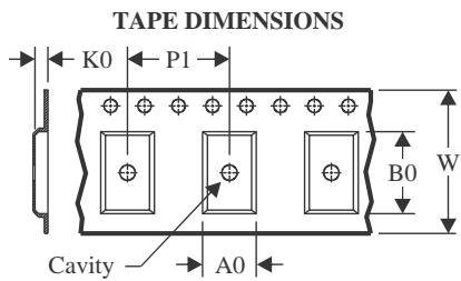
| A0 | Dimension designed to accommodate the component width |
| B0 | Dimension designed to accommodate the component length |
| K0 | Dimension designed to accommodate the component thickness |
| W | Overall width of the carrier tape |
| P1 | Pitch between successive cavity centers |
Reel Width (W1)
QUADRANT ASSIGNMENTS FOR PIN 1 ORIENTATION IN TAPE
*All dimensions are nomina
| Device | Package Type | Package Drawing | Pins | SPQ | Reel Diameter (mm) | Reel Width W1 (mm) | A0 (mm) | B0 (mm) | K0 (mm) | P1 (mm) | W (mm) | Pin1 Quadrant |
| DRV8876PWPR | HTSSOP | PWP | 16 | 2000 | 330.0 | 12.4 | 6.9 | 5.6 | 1.6 | 8.0 | 12.0 | Q1 |
| DRV8876PWPRG4 | HTSSOP | PWP | 16 | 2000 | 330.0 | 12.4 | 6.9 | 5.6 | 1.6 | 8.0 | 12.0 | Q1 |
| DRV8876RGTR | VQFN | RGT | 16 | 3000 | 330.0 | 12.4 | 3.3 | 3.3 | 1.1 | 8.0 | 12.0 | Q2 |
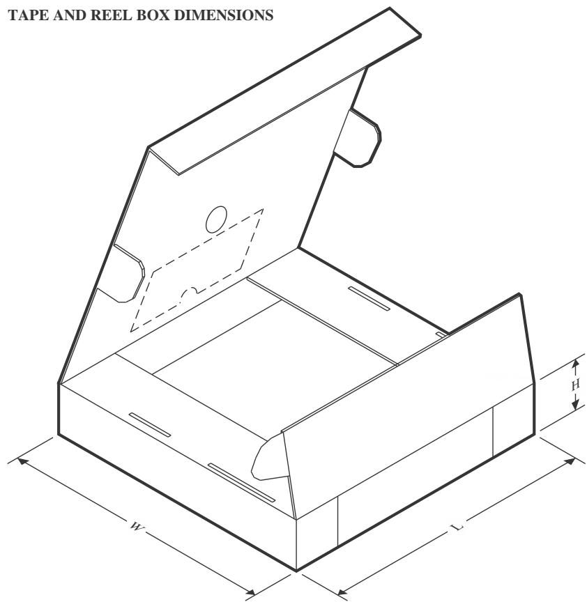
*All dimensions are nominal
| Device | Package Type | Package Drawing | Pins | SPQ | Length (mm) | Width (mm) | Height (mm) |
| DRV8876PWPR | HTSSOP | PWP | 16 | 2000 | 350.0 | 350.0 | 43.0 |
| DRV8876PWPRG4 | HTSSOP | PWP | 16 | 2000 | 350.0 | 350.0 | 43.0 |
| DRV8876RGTR | VQFN | RGT | 16 | 3000 | 367.0 | 367.0 | 35.0 |
PLASTIC SMALL OUTLINE

Images above are just a representation of the package family, actual package may vary. Refer to the product data sheet for package details.
4073225-3/J
PLASTIC SMALL OUTLINE

NOTES:
PowerPAD is a trademark of Texas Instruments.
PLASTIC SMALL OUTLINE
NOTES: (continued)
Publication IPC-7351 may have alternate designs.
Solder mask tolerances between and around signal pads can vary based on board fabrication site.
This package is designed to be soldered to a thermal pad on the board. For more information, see Texas Instruments literature numbers SLMA002 (www.ti.com/lit/slma002) and SLMA004 (www.ti.com/lit/slma004).
Size of metal pad may vary due to creepage requirement.
PLASTIC SMALL OUTLINE
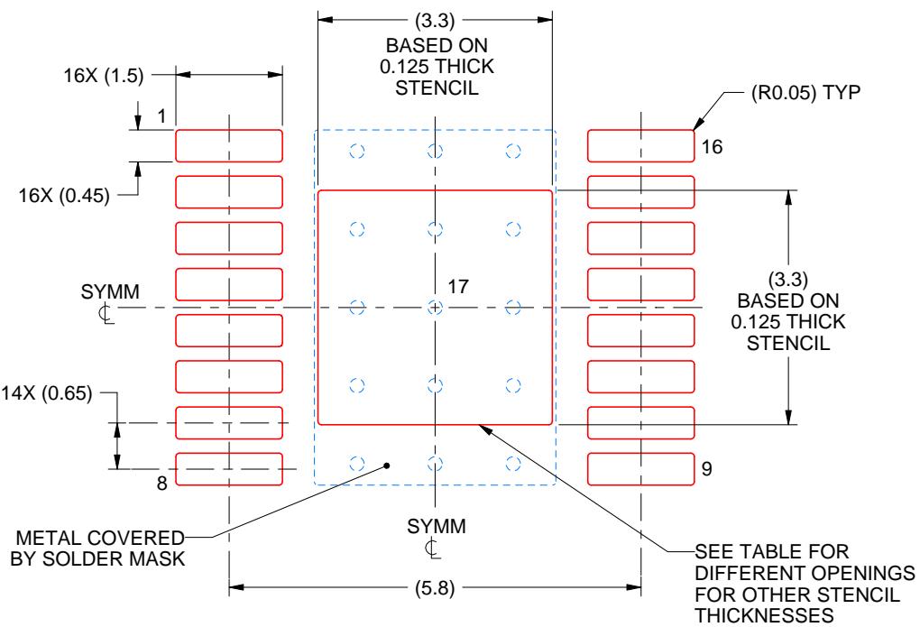
SOLDER PASTE EXAMPLE EXPOSED PAD 100% PRINTED SOLDER COVERAGE BY AREA SCALE:10X
| STENCIL THICKNESS | SOLDER STENCIL OPENING |
| 0.1 | 3.69 X 3.69 |
| 0.125 | 3.3 X 3.3 (SHOWN) |
| 0.15 | 3.01 X 3.01 |
| 0.175 | 2.79 X 2.79 |
4214868/A 02/2017
NOTES: (continued)
Laser cutting apertures with trapezoidal walls and rounded corners may offer better paste release. IPC-7525 may have alternate design recommendations.
Board assembly site may have different recommendations for stencil design.
PLASTIC QUAD FLATPACK - NO LEAD
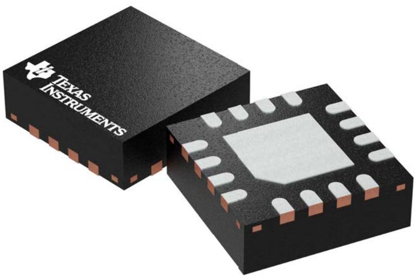
Images above are just a representation of the package family, actual package may vary. Refer to the product data sheet for package details.
4203495/I
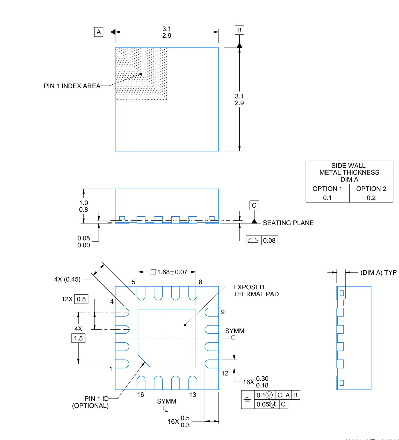
NOTES:
All linear dimensions are in millimeters. Any dimensions in parenthesis are for reference only. Dimensioning and tolerancing per ASME Y14.5M.
This drawing is subject to change without notice.
The package thermal pad must be soldered to the printed circuit board for thermal and mechanical performance.
4222419/E 07/2025
NOTES: (continued)

This package is designed to be soldered to a thermal pad on the board. For more information, see Texas Instruments literature number SLUA271 (www.ti.com/lit/slua271).
Vias are optional depending on application, refer to device data sheet. If any vias are implemented, refer to their locations shown on this view. It is recommended that vias under paste be filled, plugged or tented.
PLASTIC QUAD FLATPACK - NO LEAD
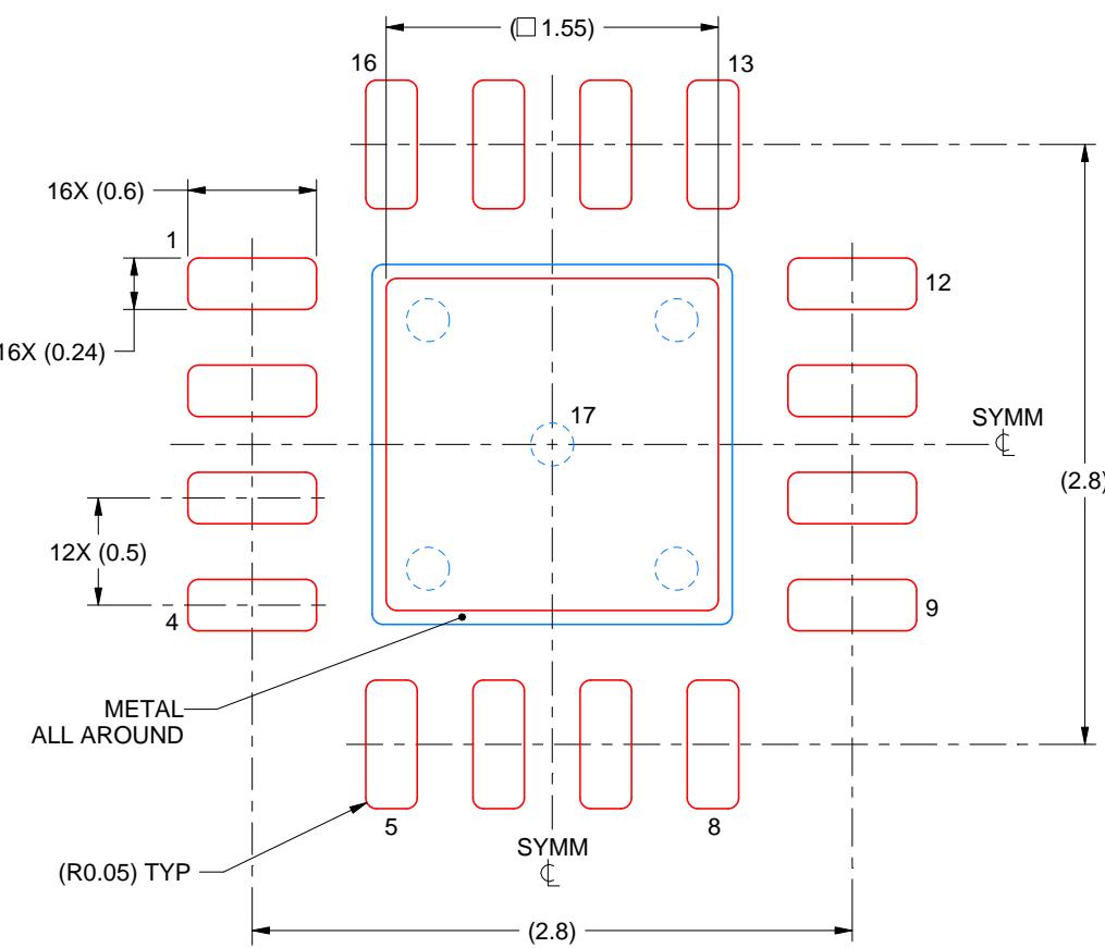
SOLDER PASTE EXAMPLE BASED ON 0.125 mm THICK STENCIL
EXPOSED PAD 17: 85% PRINTED SOLDER COVERAGE BY AREA UNDER PACKAGE SCALE:25X
4222419/E 07/2025
NOTES: (continued)
- Laser cutting apertures with trapezoidal walls and rounded corners may offer better paste release. IPC-7525 may have alternate design recommendations.
Figures and diagrams from the PDF
Preview the extracted datasheet assets and open any image in a separate tab for closer inspection.



















Use this datasheet from any agent
Send the page, markdown, chunks, or search endpoint to ChatGPT, Claude, embedr-app, or your own tooling.