
NAU7802
Precision low-power 24-bit sigma-delta ADC with programmable gain amplifier, dual differential inputs, onboard oscillator, temperature sensor, and I2C-compatible 2-wire interface.
NAU7802 Precision ADC with 2-wire Control Interface
1 GENERAL DESCRIPTION
The Nuvoton NAU7802 is a precision low-power 24-bit analog-to-digital converter (ADC), with an onboard low-noise programmable gain amplifier (PGA), onboard RC or Crystal oscillator, and a precision 24-bit sigma-delta (Σ-Δ) analog to digital converter (ADC). The NAU7802 device is capable of up to 23-bit ENOB (Effective Number of Bits) performance. This device provides a complete front-end solution for bridge/sensor measurement such as in weigh scales, strain gauges, and many other high resolution, low sample rate applications.
The many built-in features enable high performance applications with very low external parts count. Additionally, both operating current and standby current are very low, and many power management features are included. These enable powering only those elements of the chip that are needed, and also, to operate at greatly reduced power if the full 23-bit ENOB performance is not required.
The Programmable Gain Amplifier (PGA) provides selectable gains from 1 to 128. The A/D conversion is performed with a Sigma-Delta modulator and programmable FIR filter that provides a simultaneous 50Hz and 60Hz notch filter to effectively improve interference immunity. Also, this device provides a standard 2-wire interface compatible with I2C protocol for simple and straightforward connection to and interoperation with a wide range of possible host processors.
2 SYSTEM BLOCK DIAGRAM
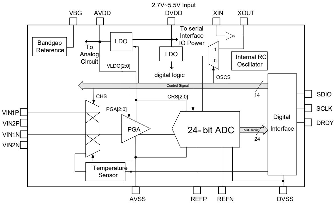
Table of Contents
1 GENERAL DESCRIPTION .... 1
2 SYSTEM BLOCK DIAGRAM .... 1
3 FEATURES .... 4
4 APPLICATIONS .... 4
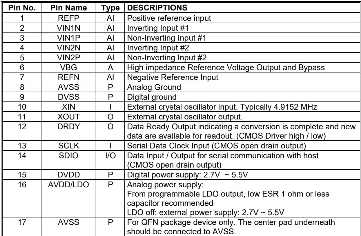
5 PIN CONFIGURATION .... 5
6 PIN DESCRIPTION .... 6
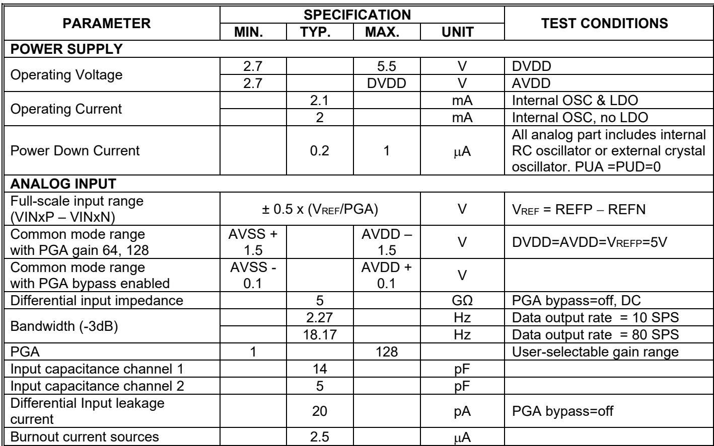
7 ELECTRICAL CHARACTERISTICS .... 7
7.1 Absolute Maximum Ratings .... 7
7.2 DC Electrical Characteristics .... 7
7.3 RC Osc and AC characteristics .... 9
7.4 Temperature Sensor .... 9
7.5 Typical Characteristics .... 10
7.5.1 NAU7802 Linearity – (Error % vs. Input Voltage).... 10
7.5.2 Noise Performance – NAU7802.... 11
7.5.3 ESD Performance – NAU7802.... 11
7.6 Digital Serial Interface Timing .... 12
7.7 Analog Input (VIN1P, VIN1N, VIN2N, VIN2P).... 12
7.8 Power Supply.... 12
7.9 2-Wire-Serial Control and Data Bus (I²C Style Interface).... 13
7.9.1 2-Wire Protocol Convention.... 13
7.9.2 2-Wire Write Operation.... 14
7.9.3 2-Wire Single Read Operation.... 15
7.10 2-Wire Timing.... 16
7.11 NAU7802 Streaming Data Mode.... 16
7.11.1 Enabling the Streaming I2C Mode.... 16
7.11.2 Streaming I2C Mode R/W Protocol 1.... 17
7.11.3 Streaming I2C Mode R/W Protocol 2.... 17
7.12 Device Calibration Features.... 17
7.12.1 Internal or External Calibration.... 18
7.12.2 Calibration Limitations.... 19
7.12.3 Calibration Error.... 19
7.13 Internal Band-Gap Circuit.... 19
7.14 Reset and Power-down Mode.... 20
7.15 Temperature Sensor.... 20
7.16 Oscillator Features.... 21
7.16.1 External Crystal Oscillator.... 21
7.16.2 External Clock Source.... 21
8 APPLICATION INFORMATION .... 22
8.1 Power-On Sequencing.... 22
8.2 Signal Path Normal Operation.... 22
8.3 Signal Path with PGA Bypass Enabled.... 23
8.4 16-pin Application Circuit .... 23
3. SUMMARY DEVICE REGISTER MAP .... 25
4. DEVICE REGISTER MAP DETAILS .... 26
4.1 REG0x00: PU_CTRL .... 26
4.2 REG0x01: CTRL1 .... 27
4.3 REG0x02: CTRL2 .... 28
4.4 REG0x03-REG0x05: Channel 1 OFFSET Calibration .... 29
4.5 REG0x06-REG0x09: Channel 1 GAIN Calibration .... 29
4.6 REG0x0A-REG0x0C: Channel 2 OFFSET Calibration .... 29
4.7 REG0x0D-REG0x10: Channel 2 GAIN Calibration .... 29
4.8 REG0x11: I2C Control .... 30
4.9 REG0x12-REG0x14: ADC Conversion Result .... 31
4.10 REG0x15: ADC registers .... 32
4.11 REG0x15-REG0x17: OTP Read Value and ADC Registers Read .... 33
4.12 REG0x18: Read Only .... 33
4.13 REG0x19: Read Only .... 33
4.14 REG0x1A: Read Only .... 33
4.15 REG0x1B: PGA Registers .... 33
4.16 REG0x1C: POWER CONTROL Register .... 34
4.17 REG0x1D: Read Only .... 34
4.18 REG0x1E: Read Only .... 34
4.19 REG0x1F: Revision ID .... 34
5 PACKAGE DIMENSIONS .... 35
5.1 SOP-16 – 150 mil.... 35
5.2 QFN-16.... 36
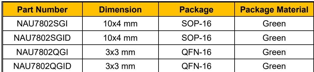
6 ORDERING INFORMATION .... 37
7 REVISION HISTORY .... 38
IMPORTANT NOTICE .... 39
3 FEATURES
• Supply Voltage: 2.7V~5.5V
• On-chip AVDD regulator for internal analog circuit or external load cell o Programmable AVDD: Off, 2.4V ~ 4.5V with eight options
• Minimum 10mA AVDD LDO output drive capability at 3.0V output voltage* 1
• 23-bit effective precision analog-to-digital converter
• Simultaneous 50Hz and 60Hz rejection (reaching -90dB)
• RMS Noise:
o 50nV in 10 SPS data output rate and PGA gain = 128
o 150nV in 80 SPS data output rate and PGA gain = 128
• Programmable PGA gains from 1 to 128
• Programmable ADC data output rates
• External differential reference voltage ranges from 0.1V ~ 5V
• System clock: External crystal oscillator or on-chip RC oscillator (4.9152Mhz)
• On-chip calibration
• On-chip power-on reset circuit
• On-chip temperature sensor
• Low Power Consumption and Programmable Power Management Options
• External 4.9152MHz Crystal oscillator
• System clock:
o Internal 4.9152MHz RC oscillator (power-on default system clock)
o External 4.9152MHz Crystal oscillator
• MCU control interface: 2-wire interface compatible with I2C protocol
• Operating Temperature: -40~85℃
• Packages:
o SOP-16 (150mil) / QFN-16
o Package is Halogen-free, RoHS-compliant and TSCA-compliant
4 APPLICATIONS
• Weigh scales
• Strain Gauge
• Industrial process control
• Liquid/gas flow control
• Pressure sensors
• Voltage monitors
5 PIN CONFIGURATION
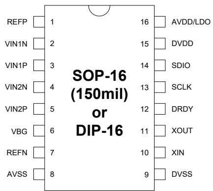
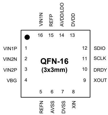
Note: QFN device center pad underneath should be connected to AVSS.
6 PIN DESCRIPTION
| Pin No. | Pin Name | Type | DESCRIPTIONS |
| 1 | REFP | AI | Positive reference input |
| 2 | VIN1N | AI | Inverting Input #1 |
| 3 | VIN1P | AI | Non-Inverting Input #1 |
| 4 | VIN2N | AI | Inverting Input #2 |
| 5 | VIN2P | AI | Non-Inverting Input #2 |
| 6 | VBG | A | High impedance Reference Voltage Output and Bypass |
| 7 | REFN | AI | Negative Reference Input |
| 8 | AVSS | P | Analog Ground |
| 9 | DVSS | P | Digital ground |
| 10 | XIN | I | External crystal oscillator input. Typically 4.9152 MHz |
| 11 | XOUT | O | External crystal oscillator output. |
| 12 | DRDY | O | Data Ready Output indicating a conversion is complete and new data are available for readout. (CMOS Driver high / low) |
| 13 | SCLK | I | Serial Data Clock Input (CMOS open drain output) |
| 14 | SDIO | I/O | Data Input / Output for serial communication with host (CMOS open drain output) |
| 15 | DVDD | P | Digital power supply: 2.7V ~ 5.5V |
| 16 | AVDD/LDO | P | Analog power supply:From programmable LDO output, low ESR 1 ohm or less capacitor recommendedLDO off: external power supply: 2.7V ~ 5.5V |
| 17 | AVSS | P | For QFN package device only. The center pad underneath should be connected to AVSS. |
TYPE description
P: Power, AI: Analog input, AO: Analog output, I: input, O: output, I/O: bi-directional
7 ELECTRICAL CHARACTERISTICS
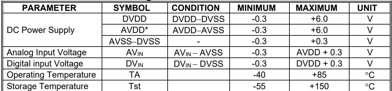
7.1 Absolute Maximum Ratings
| PARAMETER | SYMBOL | CONDITION | MINIMUM | MAXIMUM | UNIT |
| DC Power Supply | DVDD | DVDD-DVSS | -0.3 | +6.0 | V |
| AVDD* | AVDD-AVSS | -0.3 | +6.0 | V | |
| AVSS-DVSS | - | -0.3 | +0.3 | V | |
| Analog Input Voltage | $AV_{IN}$ | $AV_{IN}-AVSS$ | -0.3 | AVDD + 0.3 | V |
| Digital input Voltage | $DV_{IN}$ | $DV_{IN}-DVSS$ | -0.3 | DVDD + 0.3 | V |
| Operating Temperature | TA | -40 | +85 | °C | |
| Storage Temperature | Tst | -55 | +150 | °C |
Note: Exposure to conditions beyond those listed under absolute maximum ratings may adversely affects the life time and reliability
* AVDD should not exceed DVDD supply voltage
7.2 DC Electrical Characteristics
(Unless otherwise specified; Typical value is tested at ${ \mathsf { T A } } { = } 2 5 ^ { \circ } { \mathsf { C } } $ , DVDD = 5V, AVDD = 5V)
| PARAMETER | SPECIFICATION | TEST CONDITIONS | |||
| MIN. | TYP. | MAX. | UNIT | ||
| POWER SUPPLY | |||||
| Operating Voltage | 2.7 | 5.5 | V | DVDD | |
| 2.7 | DVDD | V | AVDD | ||
| Operating Current | 2.1 | mA | Internal OSC & LDO | ||
| 2 | mA | Internal OSC, no LDO | |||
| Power Down Current | 0.2 | 1 | μA | All analog part includes internal RC oscillator or external crystal oscillator. PUA =PUD=0 | |
| ANALOG INPUT | |||||
| Full-scale input range (VINxP - VINxN) | ± 0.5 x (VREF/PGA) | V | VREF=REFP-REFN | ||
| Common mode range with PGA gain 64, 128 | AVSS + 1.5 | AVDD - 1.5 | V | DVDD=AVDD=VREFP=5V | |
| Common mode range with PGA bypass enabled | AVSS - 0.1 | AVDD + 0.1 | V | ||
| Differential input impedance | 5 | GΩ | PGA bypass=off, DC | ||
| Bandwidth (-3dB) | 2.27 | Hz | Data output rate = 10 SPS | ||
| 18.17 | Hz | Data output rate = 80 SPS | |||
| PGA | 1 | 128 | User-selectable gain range | ||
| Input capacitance channel 1 | 14 | pF | |||
| Input capacitance channel 2 | 5 | pF | |||
| Differential Input leakage current | 20 | pA | PGA bypass=off | ||
| Burnout current sources | 2.5 | μA | |||
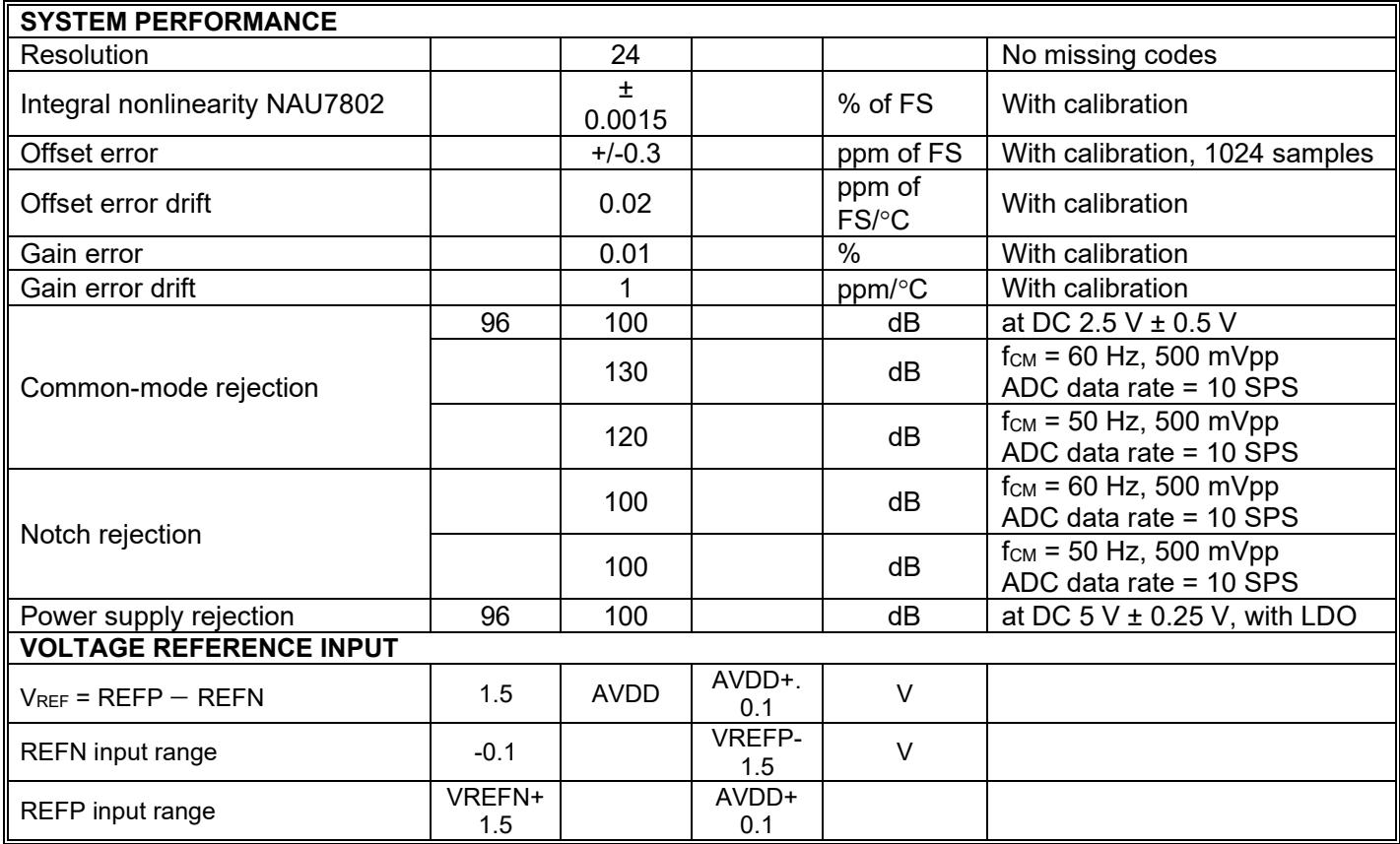
| SYSTEM PERFORMANCE | |||||
| Resolution | 24 | No missing codes | |||
| Integral nonlinearity NAU7802 | ±0.0015 | % of FS | With calibration | ||
| Offset error | +/-0.3 | ppm of FS | With calibration, 1024 samples | ||
| Offset error drift | 0.02 | ppm of FS/°C | With calibration | ||
| Gain error | 0.01 | % | With calibration | ||
| Gain error drift | 1 | ppm/°C | With calibration | ||
| Common-mode rejection | 96 | 100 | dB | at DC 2.5 V ± 0.5 V | |
| 130 | dB | $f_{CM}$ =60 Hz, 500 mVppADC data rate = 10 SPS | |||
| 120 | dB | $f_{CM}$ =50 Hz, 500 mVppADC data rate = 10 SPS | |||
| Notch rejection | 100 | dB | $f_{CM}$ =60 Hz, 500 mVppADC data rate = 10 SPS | ||
| 100 | dB | $f_{CM}$ =50 Hz, 500 mVppADC data rate = 10 SPS | |||
| Power supply rejection | 96 | 100 | dB | at DC 5 V ± 0.25 V, with LDO | |
| VOLTAGE REFERENCE INPUT | |||||
| $V_{REF}$ =REFP-REFN | 1.5 | AVDD | AVDD+.0.1 | V | |
| REFN input range | -0.1 | VREFP-1.5 | V | ||
| REFP input range | VREFN+1.5 | AVDD+0.1 | |||
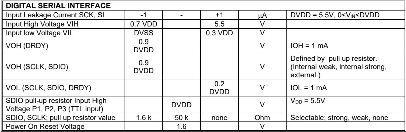
| DIGITAL SERIAL INTERFACE | |||||
| Input Leakage Current SCK, SI | -1 | - | +1 | μA | DVDD = 5.5V, 0 |
| Input High Voltage VIH | 0.7 VDD | 5.5 | V | ||
| Input low Voltage VIL | DVSS | 0.3 VDD | V | ||
| VOH (DRDY) | 0.9DVDD | V | IOH = 1 mA | ||
| VOH (SCLK, SDIO) | 0.9DVDD | V | Defined by pull up resistor.(Internal weak, internal strong,external.) | ||
| VOL (SCLK, SDIO, DRDY) | 0.2DVDD | V | IOL = 1 mA | ||
| SDIO pull-up resistor Input HighVoltage P1, P2, P3 (TTL input) | DVDD | V | $V_{DD}$ = 5.5V | ||
| SDIO, SCLK; pull up resistor value | 1.6 k | 50 k | none | Ohm | Selectable; strong, weak, none |
| Power On Reset Voltage | 1.6 | V | |||
7.3 RC Osc and AC characteristics
| Parameter | Specification (reference) | Test Conditions | |||
| Min. | Typ. | Max. | Unit | ||
| 4.9152 MHz On-chip RC oscillator | +/-3 | % | DVDD = 5V, T=25C; NAU7802 only | ||
| $T_{RDY}$ : Analog part wakeup stable plus Data Ready after exiting power-down mode | 600 | ms | DVDD = 5V; at 10 S/sec(5 sample times plus 100 ms) | ||
7.4 Temperature Sensor
| Parameter | Specification (reference) | Test Conditions | |||
| Min. | Typ. | Max. | Unit | ||
| Temperature sensor output | 109 | mV | at 25°C, @PGA=2 | ||
| Temperature sensor delta coefficient | 360 | uV / °C | relative to 25°C | ||
7.5 Typical Characteristics
7.5.1 NAU7802 Linearity – (Error % vs. Input Voltage) AVDD = 4.5V / PGA gain = 1x
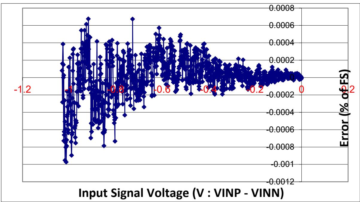
• NAU7802 Linearity Performance is symmetric, from the differential input voltage -1.2V to 0V and from 0V to 1.2V. One-sided linearity performance result is shown.
7.5.2 Noise Performance – NAU7802
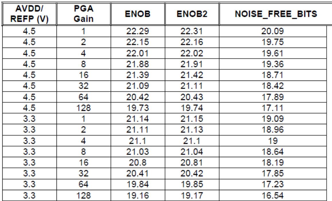
NAU7802 with LDO and Cfilter=330pF on VIN2P & VIN2N at 10 S/sec
| AVDD/ REFP (V) | PGA Gain | ENOB | ENOB2 | NOISE_FREE_BITS |
| 4.5 | 1 | 22.29 | 22.31 | 20.09 |
| 4.5 | 2 | 22.15 | 22.16 | 19.75 |
| 4.5 | 4 | 22.01 | 22.02 | 19.61 |
| 4.5 | 8 | 21.88 | 21.91 | 19.36 |
| 4.5 | 16 | 21.39 | 21.42 | 18.71 |
| 4.5 | 32 | 21.09 | 21.11 | 18.42 |
| 4.5 | 64 | 20.42 | 20.43 | 17.89 |
| 4.5 | 128 | 19.73 | 19.74 | 17.11 |
| 3.3 | 1 | 21.14 | 21.15 | 19.09 |
| 3.3 | 2 | 21.11 | 21.13 | 18.96 |
| 3.3 | 4 | 21.1 | 21.1 | 19 |
| 3.3 | 8 | 21.03 | 21.04 | 18.64 |
| 3.3 | 16 | 20.8 | 20.81 | 18.19 |
| 3.3 | 32 | 20.41 | 20.42 | 17.85 |
| 3.3 | 64 | 19.84 | 19.85 | 17.23 |
| 3.3 | 128 | 19.16 | 19.17 | 16.54 |
7.5.3 ESD Performance – NAU7802
| Test Method | PD | PS | ND | NS | Remark |
| HBM | 4kV | 4kV | -4kV | -4kV | Pass |
| MM | 400V | 400V | -400V | -400V | Pass |
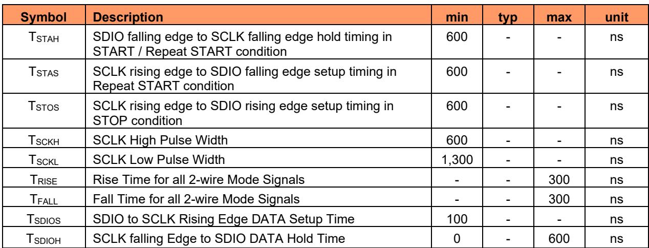
7.6 Digital Serial Interface Timing
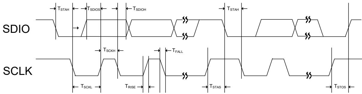
Two-wire Control Mode Timing
| Symbol | Description | min | typ | max | unit |
| $T_{STAH}$ | SDIO falling edge to SCLK falling edge hold timing in START / Repeat START condition | 600 | - | - | ns |
| $T_{STAS}$ | SCLK rising edge to SDIO falling edge setup timing in Repeat START condition | 600 | - | - | ns |
| $T_{STOS}$ | SCLK rising edge to SDIO rising edge setup timing in STOP condition | 600 | - | - | ns |
| $T_{SCKH}$ | SCLK High Pulse Width | 600 | - | - | ns |
| $T_{SCKL}$ | SCLK Low Pulse Width | 1,300 | - | - | ns |
| $T_{RISE}$ | Rise Time for all 2-wire Mode Signals | - | - | 300 | ns |
| $T_{FALL}$ | Fall Time for all 2-wire Mode Signals | - | - | 300 | ns |
| $T_{SDIOS}$ | SDIO to SCLK Rising Edge DATA Setup Time | 100 | - | - | ns |
| $T_{SDIOH}$ | SCLK falling Edge to SDIO DATA Hold Time | 0 | - | 600 | ns |
7.7 Analog Input (VIN1P, VIN1N, VIN2N, VIN2P)
The input signal to be measured is applied to one of two differential input signal pairs. The desired signal pair is selected using an analog input multiplexer, which is controlled by settings in the device command and control registers.
This device is optimized to accept differential input signals, but can also measure single-ended signals. When measuring single-ended signals with respect to ground, connect the negative input (VIN1N or VIN2N) to ground and connect the input signal to the positive input (VIN1P or VIN2P). Note that when this device is configured this way, only half of the converter full-scale range is used, since only positive digital output codes are produced.
7.8 Power Supply
The digital power supply DVDD should use the same power source as used for the host processor supporting the digital interface communication. The analog power supply AVDD can be provided by external regulator output (power-on default setting) or provided by a built-in voltage regulator. The eight programmable output voltage levels of the built-in regulator are: off (High-Z output, default power-on setting), 2.4V, 2.7V, 3.0V 3.3V, 3.6V, 4.2V, and 4.5V. This output is intended to provide the driving current for external sensors such as load cells for weight measurement applications.
7.9 2-Wire-Serial Control and Data Bus (I2C Style Interface)
The serial interface provides a 2-wire bidirectional read/write data interface similar to and typically compatible with standard I2C protocol. This protocol defines any device that sends CLK onto the bus as a master, and the receiving device as slave. The NAU7802 can function only as a slave device.
An external clock drives the device, and in accordance with the protocol, data is sent to or from the device accordingly. All functions are controlled by means of a register control interface in the device. Additionally, a "data ready" output pin – DRDY pin is provided to indicate to the host that a new conversion has been completed and that data are ready to be read from the device. The host may either use this signal or poll device register Reg0x00[5] CR bit to determine when new data are available.
7.9.1 2-Wire Protocol Convention
All 2-Wire interface operations must begin with a START condition, which is a HIGHto-LOW transition of SDIO while SCLK is HIGH. All 2-Wire interface operations are terminated by a STOP condition, which is a LOW to HIGH transition of SDIO while SCLK is HIGH. A STOP condition at the end of a read or write operation places the serial interface in standby mode.
An acknowledge (ACK), is a software convention is used to indicate a successful data transfer. To allow for the ACK response, the transmitting device releases the SDIO bus after transmitting eight bits. During the ninth clock cycle, the receiver pulls the SDIO line LOW to acknowledge the reception of the eight bits of data.
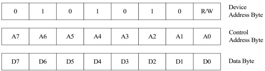
Following a START condition, the master must output a device address byte. This consists of a 7-bit device address, and the LSB of the device address byte is the R/W (Read/Write) control bit. When R/W=1, this indicates the master is initiating a read operation from the slave device, and when R/W=0, the master is initiating a write operation to the slave device. If the device address matches the address of the slave device, the slave will output an ACK during the period when the master allows for the ACK signal.
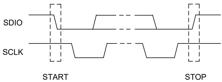
Figure 1: START and STOP
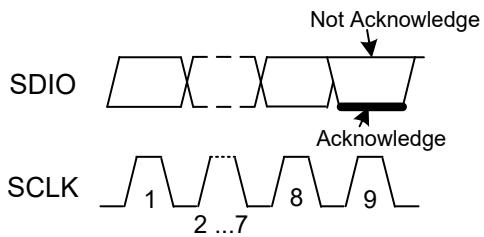
Figure 2: Acknowledge and NOT Acknowledge
| 0 | 1 | 0 | 1 | 0 | 1 | 0 | R/W | DeviceAddress Byte |
| A7 | A6 | A5 | A4 | A3 | A2 | A1 | A0 | ControlAddress Byte |
| D7 | D6 | D5 | D4 | D3 | D2 | D1 | D0 | Data Byte |
Figure 3: Slave Address Byte, Control Address Byte, and Data Byte
Figure 4: A complete 2 wire write 1 control register sequence
7.9.2 2-Wire Write Operation
A Write operation consists of a two-byte instruction followed by one or more Data Bytes. A Write operation requires a START condition, followed by a valid device address byte with R/W=0, a valid control address byte, data byte(s), and a STOP condition.
When more than one Data Byte is written, this is known as a "burst write" operation. In this operation, the host may write sequential bytes of information simply by transmitting a new data byte after each ACK from the NAU7802. The NAU7802 automatically increments the register address by one for each subsequent byte-write operation. This will continue until the STOP condition is met.
The NAU7802 is permanently programmed with “010 1010” (0x2A) as the Device Address. If the Device Address matches this value, the NAU7802 will respond with the expected ACK signaling as it accepts the data being transmitted into it.

Figure 5: Single Write Sequence

Figure 6: Burst Write Sequence
7.9.3 2-Wire Single Read Operation
A Read operation consists of a three-byte Write instruction followed by a Read instruction of one or more data bytes. The bus master initiates the operation issuing the following sequence: a START condition, device address byte with the R/W bit set to “0”, and a Control Register Address byte. This indicates to the slave device which of its control registers is to be accessed.
The NAU7802 is permanently programmed with “010 1010” (0x2A) as its device address. If the device address matches this value, the NAU7802 will respond with the expected ACK signaling as it accepts the Control Register Address being transmitted into it. After this, the master transmits a second START condition, and a second instantiation of the same device address, but now with R/W=1.
After again recognizing its device address, the NAU7802 transmits an ACK, followed by a one-byte value containing the data from the selected control register inside the NAU7802. During this phase, the master generates the ACK signaling with each byte transferred from the NAU7802. If there is no STOP signal from the master, the NAU7802 will internally auto-increment the target Control Register Address and then output the data bytes for this next register in the sequence.
This process will continue while the Master continues to issue ACK signaling. If the Control Register Address being indexed inside the NAU7802 reaches the value 0x7F (hexadecimal) and the value for this register is output, the index will roll over to 0x00. The data bytes will continue to be output until the master terminates the read operation by issuing a STOP condition.
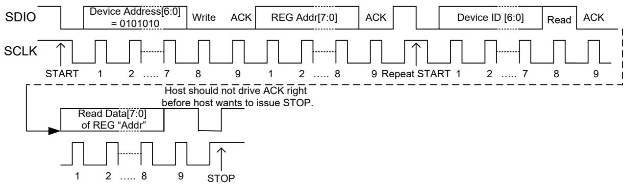
Figure 7: Single Read Sequence
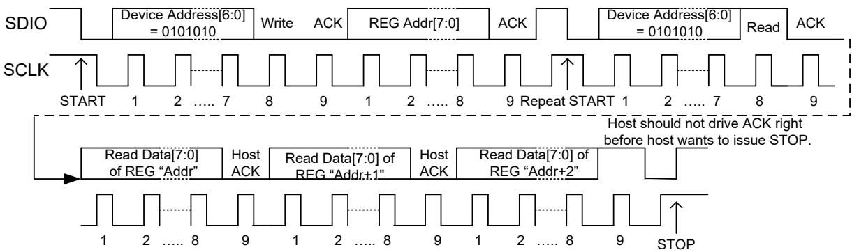
Figure 8: Burst Read Sequence
7.10 2-Wire Timing
The NAU7802 is compatible with serial clock speeds defined as “standard mode” with SCLK 0 - 100 kHz, and “fast mode” with SCLK 0 - 400 kHz. At these speeds the total bus line capacitance load is required to be 400 pF or less.
Open collector drivers are required for the serial interface. Therefore, the bus line rise time is determined by the total serial bus capacitance and the DVDD pull-up resistors. The NAU7802 defaults to a weak pull up (typical 50 k ohm) for applications with no external pull up resistor. Register 0x11 bits 5:4 provide other options including a strong internal pull-up (typical 1.6 k ohm) or no internal pull-up resistor.
7.11NAU7802 Streaming Data Mode
7.11.1 Enabling the Streaming I2C Mode
• Power Up the chip
o Write 0x00 = 0x06 (PU analog and PU digital)
o (read back 0x00 bit 3 to make sure chip is powered up)
• Enable Streaming I2C Mode
o Write REG11[7] =1 to enable streaming mode 1, or Write REG11[7] =1 and REG11[6]=1 and REG15[7]=1 to enable streaming mode 2
o (read back 0x1D bit 7 to make sure the streaming I2C mode is active)
7.11.2 Streaming I2C Mode R/W Protocol 1
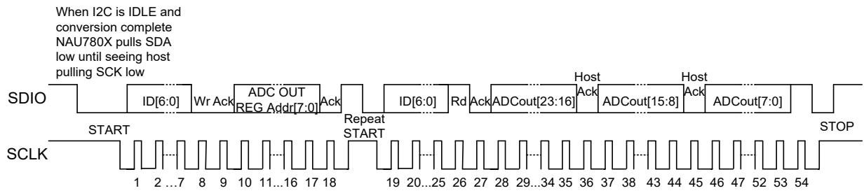
When REG0x11[7] CRSD=1, I2C is IDLE and a conversion is complete, NAU7802 will pull SDA/SDIO low to inform the host a conversion is complete. Host should respond by pulling SDA/SDIO low and pulling SCK low to initial an I2C “start” condition. When seeing SCK pulled low by host, NAU7802 will release the SDA/SDIO. Host can continue the standard I2C transaction with NAU7802
7.11.3 Streaming I2C Mode R/W Protocol 2
In addition to CASE1 REG11[7] =1, if REG0x11[6] FRD=1 and REG0x15[7]=1, host can direct issue a I2C read cycle (No writing register address first needed), after the ACK bit for the ID and “Read Select”, the following 24 SCK is used for NAU7802 to shift out the 24 bit ADC conversion result without the ACK bit needed. So the total Read ADC conversion data cycle can be shortened to 33 SCK comparing to 54 SCK plus a repeat start by using the standard I2C.
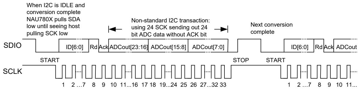
Note: Write NAU7802 register is always allowed by using Standard I2C write NAU7802 register protocol. So these two special bits can be reset to 0 to return to Standard I2C protocol
7.12Device Calibration Features
Calibration is not required for low accuracy applications, but may be needed in sensitive applications. When calibration is used the system designer has three options.
Calibration can be performed at the system level with an external processor or at the ADC device. Inside the ADC device both internal and external calibration can be performed.
Internal ADC device calibration only removes internal PGA gain and offset errors.
External ADC device calibration removes DC errors at the device input pins and the internal PGA gain and offset errors.
As with all devices of this type, the NAU7802 internal gain factors and offset voltages will contain small errors owing to fabrication process variations, power supply voltage changes, and temperature variations. The same types of errors exist at the external system level.
These errors can be measured by the NAU7802 device itself using the calibration features. After calibration, the stored values in the calibration registers are automatically added/subtracted to the data from the ADC before being output as the ADC resulting data. It is recommended to calibrate the NAU8702 after the following conditions:
• Initial power-up
• Power-up after long-duration register mediated power-down conditions
• PGA gain changes
• Supply changes
• Significant temperature changes (can be measured using built-in thermal sensing feature)
• Sample rate changes
• Channel select changes
Calibration is initiated by writing 1 to Reg0x02[2] CALS bit. CALS then becomes a status bit that can be read to know when calibration is complete. Calibration type is defined by Reg0x02[1:0] CALMOD bits. CALS will remain Logic=1 during calibration, and will read back as Logic=0 when calibration is completed.
After calibration, it is important to check the Reg0x02[3] CAL_ERR status bit to determine if there was any problem during calibration. If there was an error, all data output could be invalid.
7.12.1 Internal or External Calibration
The internal calibration disconnects the inputs from the input pins and internally connects the differential inputs to the same internal voltage reference point for calibration. External calibration uses the inputs as-is, and it is up to the system designer to configure them appropriately for the calibration procedure. The resulting gain or offset calibration value is stored in the selected calibration register. The same register sets are used for both internal or external calibration and it is intended that only one choice of internal/external calibration is used at any given time.
At all times, when reading a value from the ADC registers, the gain and offset calibration values are added/subtracted to the ADC value before being output. The default values for the calibration registers is zero, so these have no effect on the ADC output value until after a calibration operation has been instantiated.
The resulting output value is calculated as:
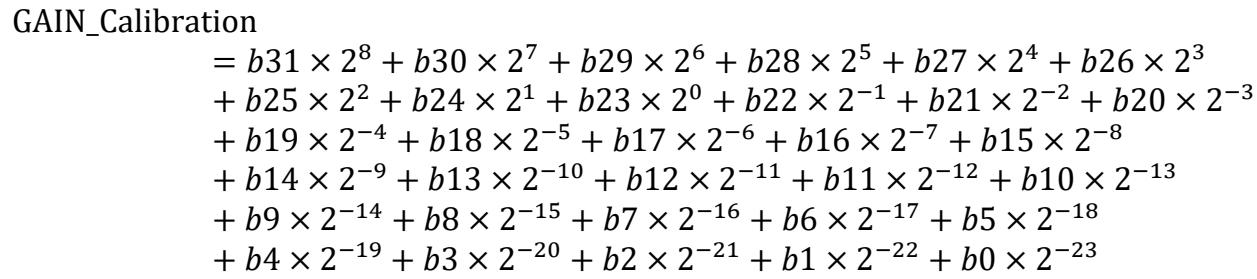
ADC Output Value = Gain_Calibration* (ADC measurement - Offset_Calibration)
Calibration Equations:
$$
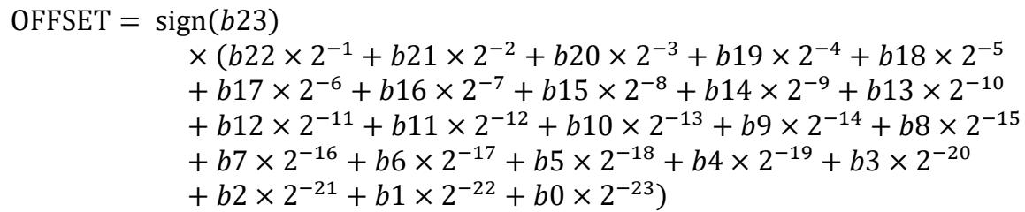
\begin{array}{r l} \text {OFFSET} = & \operatorname{sign} (b 2 3) \ & \times (b 2 2 \times 2 ^ {- 1} + b 2 1 \times 2 ^ {- 2} + b 2 0 \times 2 ^ {- 3} + b 1 9 \times 2 ^ {- 4} + b 1 8 \times 2 ^ {- 5} \ & + b 1 7 \times 2 ^ {- 6} + b 1 6 \times 2 ^ {- 7} + b 1 5 \times 2 ^ {- 8} + b 1 4 \times 2 ^ {- 9} + b 1 3 \times 2 ^ {- 1 0} \ & + b 1 2 \times 2 ^ {- 1 1} + b 1 1 \times 2 ^ {- 1 2} + b 1 0 \times 2 ^ {- 1 3} + b 9 \times 2 ^ {- 1 4} + b 8 \times 2 ^ {- 1 5} \ & + b 7 \times 2 ^ {- 1 6} + b 6 \times 2 ^ {- 1 7} + b 5 \times 2 ^ {- 1 8} + b 4 \times 2 ^ {- 1 9} + b 3 \times 2 ^ {- 2 0} \ & + b 2 \times 2 ^ {- 2 1} + b 1 \times 2 ^ {- 2 2} + b 0 \times 2 ^ {- 2 3}) \end{array}
$$
$$
\begin{array}{r l} & {\mathrm {GAIN_Calibration}} \ & {\quad = b 3 1 \times 2 ^ {8} + b 3 0 \times 2 ^ {7} + b 2 9 \times 2 ^ {6} + b 2 8 \times 2 ^ {5} + b 2 7 \times 2 ^ {4} + b 2 6 \times 2 ^ {3}} \ & {\quad + b 2 5 \times 2 ^ {2} + b 2 4 \times 2 ^ {1} + b 2 3 \times 2 ^ {0} + b 2 2 \times 2 ^ {- 1} + b 2 1 \times 2 ^ {- 2} + b 2 0 \times 2 ^ {- 3}} \ & {\quad + b 1 9 \times 2 ^ {- 4} + b 1 8 \times 2 ^ {- 5} + b 1 7 \times 2 ^ {- 6} + b 1 6 \times 2 ^ {- 7} + b 1 5 \times 2 ^ {- 8}} \ & {\quad + b 1 4 \times 2 ^ {- 9} + b 1 3 \times 2 ^ {- 1 0} + b 1 2 \times 2 ^ {- 1 1} + b 1 1 \times 2 ^ {- 1 2} + b 1 0 \times 2 ^ {- 1 3}} \ & {\quad + b 9 \times 2 ^ {- 1 4} + b 8 \times 2 ^ {- 1 5} + b 7 \times 2 ^ {- 1 6} + b 6 \times 2 ^ {- 1 7} + b 5 \times 2 ^ {- 1 8}} \ & {\quad + b 4 \times 2 ^ {- 1 9} + b 3 \times 2 ^ {- 2 0} + b 2 \times 2 ^ {- 2 1} + b 1 \times 2 ^ {- 2 2} + b 0 \times 2 ^ {- 2 3}} \end{array}
$$
$$
\operatorname{sign} (\mathrm{b} 2 3) = 1 \text { if } \mathrm{b} 2 3 = 0; \operatorname{sign} (\mathrm{b} 2 3) = - 1 \text { if } \mathrm{b} 2 3 = 1.
$$
$$
\mathrm{DOUT} \langle 2 3: 0 \rangle^ {\prime} = (\mathrm{DOUT} \langle 2 3: 0 \rangle + \mathrm{OFFSET} \langle 2 3: 0 \rangle) \times \text { GAIN_Calibration } \langle 3 1: 0 \rangle
$$
7.12.2 Calibration Limitations
Note that the offset that is trimmed from the input is mapped through the gain register. Additionally:
• Calibration can be limited by signal headroom in the analog path
• With the converters intrinsic gain & offset error the minimal full scale input range may be higher or lower.
7.12.3 Calibration Error
A calibration error may occur during gain calibration when one of the following happens:
• The gain required to map input to full scale is larger than the range available in the gain register ~ 256
• The offset adjusted input is negative, e.g. 256 > gain > 0
If there is a calibration error, CAL_ERR will set to Logic=1 when the calibration sequence is completed. Once CAL_ERR is set to Logic=1, it will remain in this state until either the NAU7802 is reset, or after a valid calibration sequence is completed.
When CAL_ERR = 1, the data in the calibration registers is invalid. It is recommended perform the calibration routine again, or to write a default value into the calibration registers.
7.13Internal Band-Gap Circuit
An internal band-gap establishes accurate operation of the device over a wide temperature range. No adjustment of the bandgap is necessary. For optimum performance, the NAU7802 makes available a band-gap output pin “VBG” which should be bypassed to ground with a high quality X7R small value 0.1 uF filter capacitor.
7.14Reset and Power-down Mode
An automatic built-in power-on reset function will reset the NAU7802 after DVDD power becomes valid. After AVDD power is stable (from external power or from the built-in regulator), reset may also be initiated at any time using the register control interface. The scope of the register based reset using register 0x00 bit 0, named “RR” set to 1, is equivalent to the poweron reset.
Power-down standby mode can be selected using the register control interface using register 0x00 bits 2:1, named “PUA” and “PUD” set to 0. This mode shuts down the entire analog portion of the part, including the 24-bit ADC, voltage regulator, PGA, bandgap reference, and internal RC oscillator (or external crystal oscillator) to reduce power consumption.
The command and control interface is static and works normally in power-down mode. Powerdown mode can be terminated at any time by changing the register controls to return the device to normal operating mode, using register 0x00 bits 2:1, named “PUA” and “PUD” set to 1. In this way the contents of the registers are retained for immediate normal use.
After reset or after resuming normal operating mode after power-down mode, the host should wait through six cycles of data conversion. This allows the device to stabilize all functions and to flush all old internal data for a full-accuracy output. This timing is automatically generated by the device for the DRDY pin and Data Ready device status bit.
7.15Temperature Sensor
A matched pair of on-chip diodes provides temperature sensing capability. Temperature sensing is selected by setting of the analog input multiplexer using the register control interface. A PGA gain of 2x or 1x is used for temperature sensing to prevent PGA clipping.
By measuring the difference in voltage of these diodes, temperature changes can be inferred from a baseline temperature. Please refer to the specification items “Temperature sensor output” and “Temperature sensor delta coefficient.”
Note: On chip temperature can be directly measured ADC and bypass PGA, when using this mode, ADC output is timed by two for correct temperature. If using PGA for temperature measurement, PGA gain needs to set 2 for correct measurement.
0x11[1]=1
// PAG input switched to temperature sensor
0x15[3:2]
0x1B[5:3]=3b’010
// set common mode to REFN or REFP and ADC gain divided by 2 // disable PGA output buffer and PGA output bypass
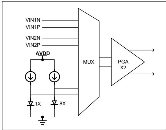
Figure 8
7.16Oscillator Features
This device may either accept an external clock, use an internal RC oscillator, or use a built-in crystal oscillator for its time base. An accurate clock is important for the digital filtering of 50Hz or 60Hz components to work optimally. The internal oscillator is trimmed at the factory for good accuracy.
The internal RC or crystal oscillator frequency may be output on the DRDY pin. This is done by programming Reg0x00[6] DRDY_SEL bit as follows:
$\mathsf { W r i t e \ R E G 0 } { \times } 0 0 [ 6 ] = 0 $ Use oscillator as system clock
• Write REG0x01[6] = 1: Output system clock on DRDY pin
7.16.1 External Crystal Oscillator
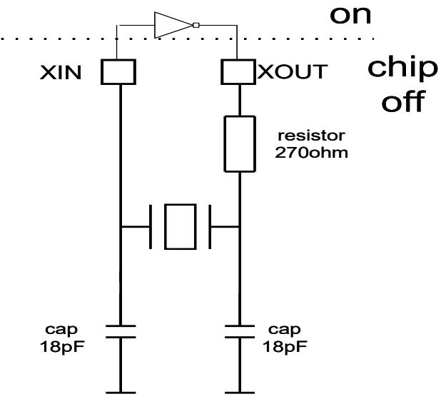
When an external 4.9152MHz crystal oscillator is used, the preferred application circuit on the XIN & XOUT pins is as shown below. The crystal oscillator could operate without the 270 Ohm resistor and without the 18pF capacitor on XIN at a reduced performance.
7.16.2 External Clock Source
When the clock for the NAU7802 may also be provided from an external source. To use this feature, the device is configured in the same way as for using a crystal and the external clock signal is applied to the XIN pin.
8 APPLICATION INFORMATION
This section includes both circuit diagram information and recommendations for programming the device. Programming is essential, as the device will not function until various default settings are changed to values appropriate for the application.
8.1 Power-On Sequencing
After the DVDD supply is valid, and after the internal power-on reset is completed, the NAU7802 is ready for host program control access. The following steps apply to most applications.
Set Reg0x00[0] RR bit to 1, to guarantee a reset of all register values.
Set Reg0x00[0] RR bit to 0 and Reg0x00[1] PUD bit to 1, to enter normal operation.
After about 200 microseconds, Reg0x00[3] PUR bit will be Logic=1 indicating the device is ready for the remaining programming setup.
At this point, all appropriate device selections and configuration can be made.
a. For example, Reg0x00 = 0xAE
b. Write Reg0x15 = 0x30
Enter the low power standby condition by writing PUA and PUD bits to 0, in Reg0x00.
Resume operation by setting PUA and PUD bits to 1, in Reg0x00. This sequence is the same for powering up from the standby condition, except that from standby all of the information in the configuration and calibration registers will be retained if the power supply is stable. Depending on conditions and the application, it may be desirable to perform calibration again to update the calibration registers for the best possible accuracy.
Please note writing 1 to Reg0x00[1] PUD bit will automatically start AD conversion. When DRDY is not ready (if DRDY pin is configured to indicate cycle ready), writing Reg0x00[4] CS bit from 0 to 1 – i.e. the transition from 0 to 1 on CS bit starts a fresh conversion. It takes 4-sample conversion time for the result to be ready in Reg0x12- 0x14, and DRDY pin show ready.
A 0 to 1 transition on CS bit during DRDY is ready has no effect on DRDY pin status. A read operation on Reg0x12 changes DRDY pin status from ready to not ready.
8.2 Signal Path Normal Operation
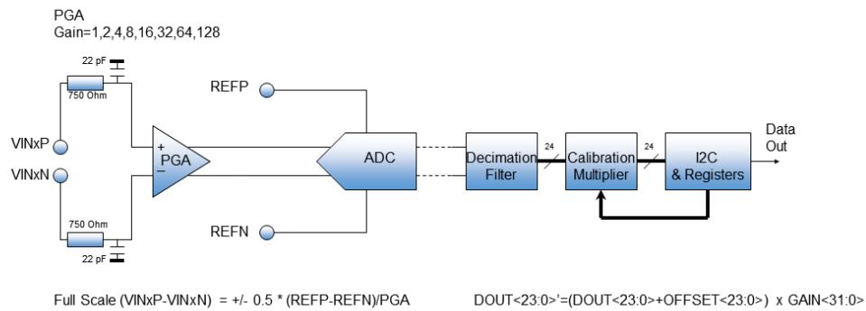
In normal operation the input signal is full scale at the ADC input when (VINxP - VINxN) = +/- 0.5 * (REFP - REFN) / PGA_Gain, within the PGA common mode range.
8.3 Signal Path with PGA Bypass Enabled
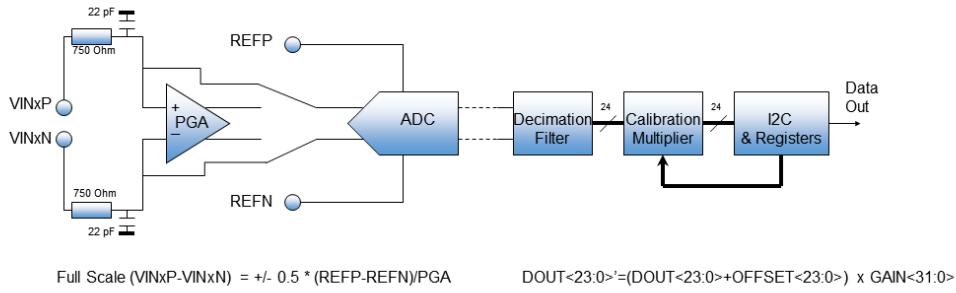
Register 0x1B bit 4, “PGA bypass enable” removes the PGA from the signal path in applications where VINxP or VINxN approach AVDD or AVSS. Because the PGA has a limited common mode input range. In this range the PGA can be bypassed.
In PGA bypass operation the input signal is full scale at the ADC input when $( V | N \times P - \dot { V } | N \times N ) = + 1 - 0 . 5 \times$ (REFP - REFN) within the ADC common mode range.
8.4 16-pin Application Circuit
The built-in voltage regulator and built-in oscillator enable very low parts count applications as shown here. The signal input filter is optional, depending on the application requirements it can be expanded with decoupling capacitors to ground if needed. With a lithium-ion battery, an external voltage regulator for the DVDD supply may also be optional.
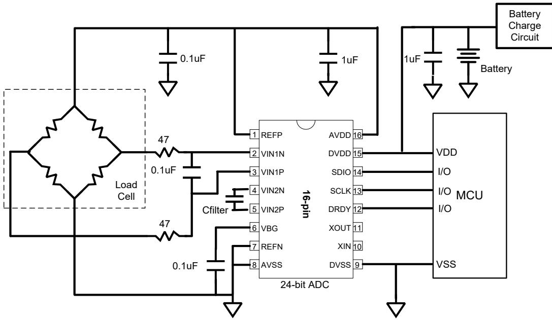
For single channel applications, Cfilter can be added for enhanced ENOB at high PGA gain settings. The filter capacitor Cfilter provides additional filtering at the PGA output. It can be enabled by setting Reg0x1C[7] PGA_CAP_EN bit to1. The following values are recommended for Cfilter:
| AVDD Supply Voltage (Volt) | 3.3 | 4.5 |
| Cfilter (pF) | 330 | 680 |
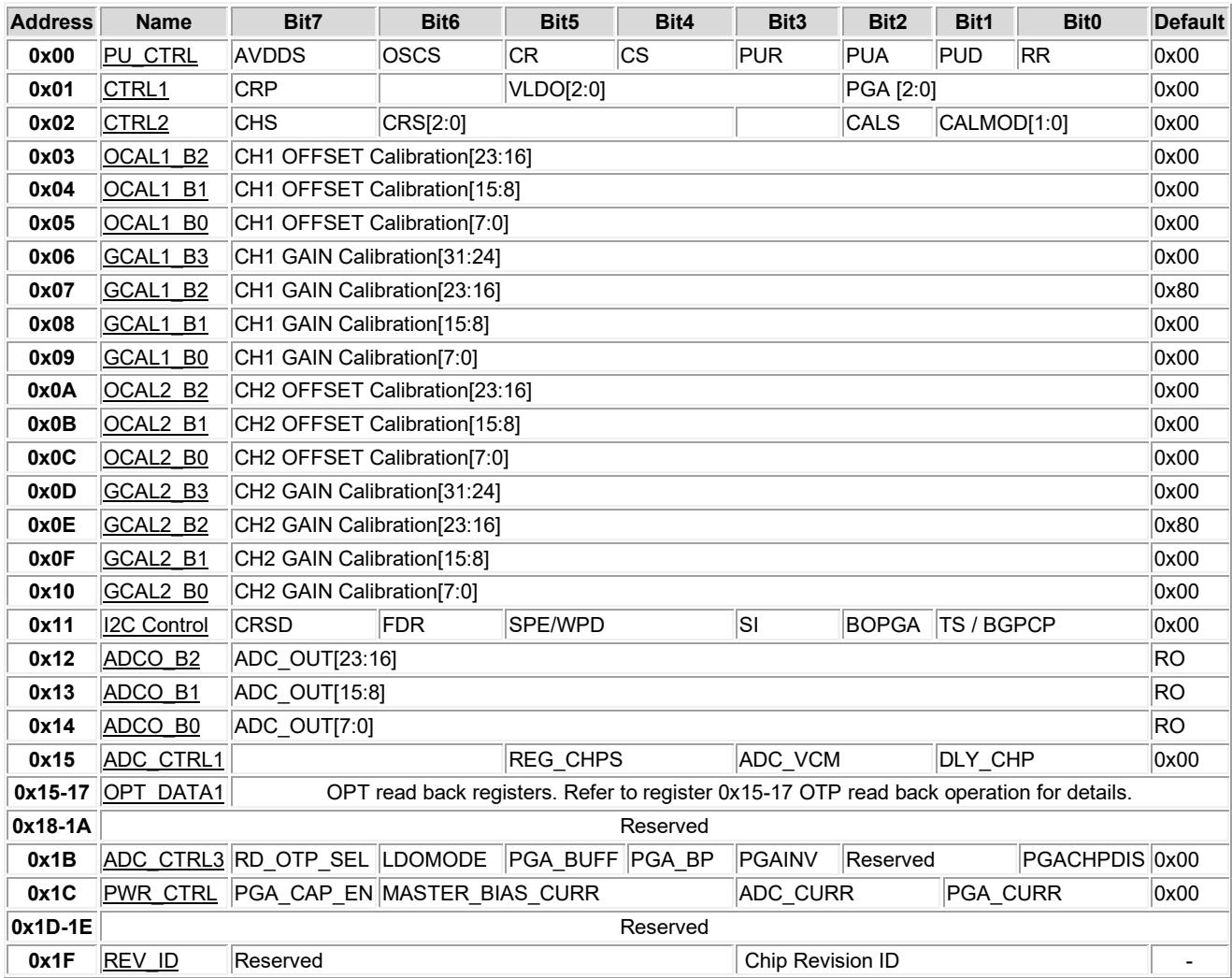
3. SUMMARY DEVICE REGISTER MAP
| Address | Name | Bit7 | Bit6 | Bit5 | Bit4 | Bit3 | Bit2 | Bit1 | Bit0 | Default |
| 0x00 | PU_CTRL | AVDDS | OSCS | CR | CS | PUR | PUA | PUD | RR | 0x00 |
| 0x01 | CTRL1 | CRP | VLDO[2:0] | PGA [2:0] | 0x00 | |||||
| 0x02 | CTRL2 | CHS | CRS[2:0] | CALS | CALMOD[1:0] | 0x00 | ||||
| 0x03 | OCAL1_B2 | CH1 OFFSET Calibration[23:16] | 0x00 | |||||||
| 0x04 | OCAL1_B1 | CH1 OFFSET Calibration[15:8] | 0x00 | |||||||
| 0x05 | OCAL1_B0 | CH1 OFFSET Calibration[7:0] | 0x00 | |||||||
| 0x06 | GCAL1_B3 | CH1 GAIN Calibration[31:24] | 0x00 | |||||||
| 0x07 | GCAL1_B2 | CH1 GAIN Calibration[23:16] | 0x80 | |||||||
| 0x08 | GCAL1_B1 | CH1 GAIN Calibration[15:8] | 0x00 | |||||||
| 0x09 | GCAL1_B0 | CH1 GAIN Calibration[7:0] | 0x00 | |||||||
| 0x0A | OCAL2_B2 | CH2 OFFSET Calibration[23:16] | 0x00 | |||||||
| 0x0B | OCAL2_B1 | CH2 OFFSET Calibration[15:8] | 0x00 | |||||||
| 0x0C | OCAL2_B0 | CH2 OFFSET Calibration[7:0] | 0x00 | |||||||
| 0x0D | GCAL2_B3 | CH2 GAIN Calibration[31:24] | 0x00 | |||||||
| 0x0E | GCAL2_B2 | CH2 GAIN Calibration[23:16] | 0x80 | |||||||
| 0x0F | GCAL2_B1 | CH2 GAIN Calibration[15:8] | 0x00 | |||||||
| 0x10 | GCAL2_B0 | CH2 GAIN Calibration[7:0] | 0x00 | |||||||
| 0x11 | I2C Control | CRSD | FDR | SPE/WPD | SI | BOPGA | TS / BGPCP | 0x00 | ||
| 0x12 | ADCO_B2 | ADC_OUT[23:16] | RO | |||||||
| 0x13 | ADCO_B1 | ADC_OUT[15:8] | RO | |||||||
| 0x14 | ADCO_B0 | ADC_OUT[7:0] | RO | |||||||
| 0x15 | ADC_CTRL1 | REG_CHPS | ADC_VCM | DLY_CHP | 0x00 | |||||
| 0x15-17 | OPT_DATA1 | OPT read back registers. Refer to register 0x15-17 OTP read back operation for details. | ||||||||
| 0x18-1A | Reserved | |||||||||
| 0x1B | ADC_CTRL3 | RD_OTP_SEL | LDOMODE | PGA_BUFF | PGA_BP | PGAINV | Reserved | PGACHPDIS | 0x00 | |
| 0x1C | PWR_CTRL | PGA_CAP_EN | MASTER_BIAS_CURR | ADC_CURR | PGA_CURR | 0x00 | ||||
| 0x1D-1E | Reserved | |||||||||
| 0x1F | REV_ID | Reserved | Chip Revision ID | - | ||||||
4. DEVICE REGISTER MAP DETAILS
4.1 REG0x00: PU_CTRL
Register Default = 0x00
| Bit | Name | Description |
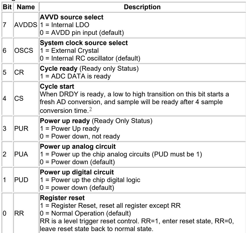
| 7 | AVDDS | AVVD source select1 = Internal LDO0 = AVDD pin input (default) |
| 6 | OSCS | System clock source select1 = External Crystal0 = Internal RC oscillator (default) |
| 5 | CR | Cycle ready (Ready only Status)1 = ADC DATA is ready |
| 4 | CS | Cycle startWhen DRDY is ready, a low to high transition on this bit starts a fresh AD conversion, and sample will be ready after 4 sample conversion time.2 |
| 3 | PUR | Power up ready (Ready Only Status)1 = Power Up ready0 = Power down, not ready |
| 2 | PUA | Power up analog circuit1 = Power up the chip analog circuits (PUD must be 1)0 = Power down (default) |
| 1 | PUD | Power up digital circuit1 = Power up the chip digital logic0 = power down (default) |
| 0 | RR | Register reset1 = Register Reset, reset all register except RR0 = Normal Operation (default)RR is a level trigger reset control. RR=1, enter reset state, RR=0, leave reset state back to normal state. |
4.2 REG0x01: CTRL1
Register Default= 0x00
| Bit | Name | Description |
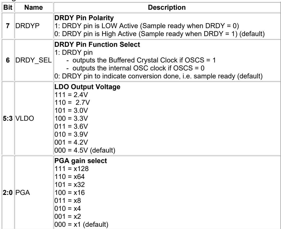
| 7 | DRDYP | DRDY Pin Polarity1: DRDY pin is LOW Active (Sample ready when DRDY = 0)0: DRDY pin is High Active (Sample ready when DRDY = 1) (default) |
| 6 | DRDY_SEL | DRDY Pin Function Select1: DRDY pin- outputs the Buffered Crystal Clock if OSCS = 1- outputs the internal OSC clock if OSCS = 00: DRDY pin to indicate conversion done, i.e. sample ready (default) |
| 5:3 | VLDO | LDO Output Voltage111 = 2.4V110 = 2.7V101 = 3.0V100 = 3.3V011 = 3.6V010 = 3.9V001 = 4.2V000 = 4.5V (default) |
| 2:0 | PGA | PGA gain select111 = x128110 = x64101 = x32100 = x16011 = x8010 = x4001 = x2000 = x1 (default) |
4.3 REG0x02: CTRL2
Register Default =0x00
| Bit | Name | Description |
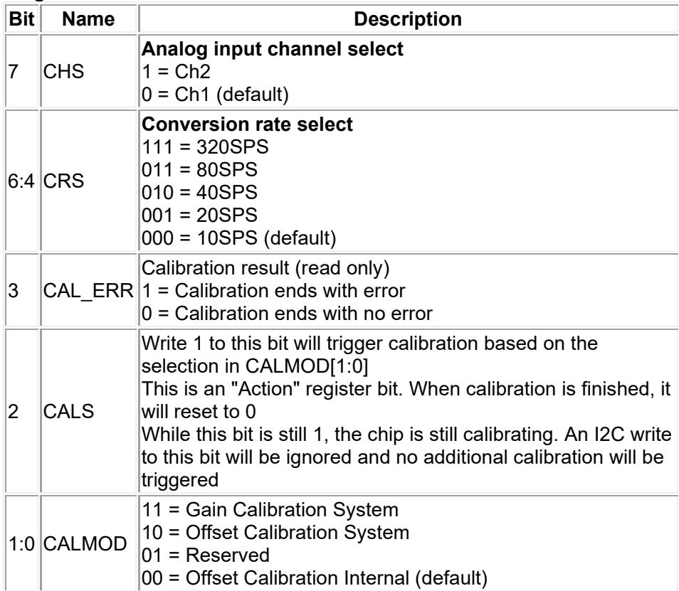
| 7 | CHS | Analog input channel select1 = Ch20 = Ch1 (default) |
| 6:4 | CRS | Conversion rate select111 = 320SPS011 = 80SPS010 = 40SPS001 = 20SPS000 = 10SPS (default) |
| 3 | CAL_ERR | Calibration result (read only)1 = Calibration ends with error0 = Calibration ends with no error |
| 2 | CALS | Write 1 to this bit will trigger calibration based on the selection in CALMOD[1:0]This is an "Action" register bit. When calibration is finished, it will reset to 0While this bit is still 1, the chip is still calibrating. An I2C write to this bit will be ignored and no additional calibration will be triggered |
| 1:0 | CALMOD | 11 = Gain Calibration System10 = Offset Calibration System01 = Reserved00 = Offset Calibration Internal (default) |
4.4 REG0x03-REG0x05: Channel 1 OFFSET Calibration
gain register
| offset register | ||||||||||||||||||||||||
| bit | 23 | 22 | 21 | 20 | 19 | 18 | 17 | 16 | 15 | 14 | 13 | 12 | 11 | 10 | 9 | 8 | 7 | 6 | 5 | 4 | 3 | 2 | 1 | 0 |
| offset | +/- | $2^{-1}$ | $2^{-2}$ | $2^{-3}$ | $2^{-4}$ | $2^{-5}$ | $2^{-6}$ | $2^{-7}$ | $2^{-8}$ | $2^{-9}$ | $2^{-10}$ | $2^{-11}$ | $2^{-12}$ | $2^{-13}$ | $2^{-14}$ | $2^{-15}$ | $2^{-16}$ | $2^{-17}$ | $2^{-18}$ | $2^{-19}$ | $2^{-20}$ | $2^{-21}$ | $2^{-22}$ | $2^{-23}$ |
| default | 0 | 0 | 0 | 0 | 0 | 0 | 0 | 0 | 0 | 0 | 0 | 0 | 0 | 0 | 0 | 0 | 0 | 0 | 0 | 0 | 0 | 0 | 0 | 0 |
4.5 REG0x06-REG0x09: Channel 1 GAIN Calibration
| bit | 31 | 30 | 29 | 28 | 27 | 26 | 25 | 24 | 23 | 22 | 21 | 20 | 19 | 18 | 17 | 16 | 15 | 14 | 13 | 12 | 11 | 10 | 9 | 8 | 7 | 6 | 5 | 4 | 3 | 2 | 1 | 0 |
| gain | $2^8$ | $2^7$ | $2^6$ | $2^5$ | $2^4$ | $2^3$ | $2^2$ | $2^1$ | $2^0$ | $2^{-1}$ | $2^{-2}$ | $2^{-2}$ | $2^{-3}$ | $2^{-4}$ | $2^{-5}$ | $2^{-6}$ | $2^{-7}$ | $2^{-8}$ | $2^{-9}$ | $2^{-10}$ | $2^{-11}$ | $2^{-12}$ | $2^{-13}$ | $2^{-14}$ | $2^{-15}$ | $2^{-16}$ | $2^{-17}$ | $2^{-18}$ | $2^{-19}$ | $2^{-20}$ | $2^{-21}$ | $2^{-22}$ |
| default | 0 | 0 | 0 | 0 | 0 | 0 | 0 | 0 | 1 | 0 | 0 | 0 | 0 | 0 | 0 | 0 | 0 | 0 | 0 | 0 | 0 | 0 | 0 | 0 | 0 | 0 | 0 | 0 | 0 | 0 | 0 | 0 |
4.6 REG0x0A-REG0x0C: Channel 2 OFFSET Calibration
Register Default = 0x000000
| offset register | |||||||||||||||||||||||||
| bit | 23 | 22 | 21 | 20 | 19 | 18 | 17 | 16 | 15 | 14 | 13 | 12 | 11 | 10 | 9 | 8 | 7 | 6 | 5 | 4 | 3 | 2 | 1 | 0 | |
| offset | +/- | $2^{-1}$ | $2^{-2}$ | $2^{-3}$ | $2^{-4}$ | $2^{-5}$ | $2^{-6}$ | $2^{-7}$ | $2^{-8}$ | $2^{-9}$ | $2^{-10}$ | $2^{-11}$ | $2^{-12}$ | $2^{-13}$ | $2^{-14}$ | $2^{-15}$ | $2^{-16}$ | $2^{-17}$ | $2^{-18}$ | $2^{-19}$ | $2^{-20}$ | $2^{-21}$ | $2^{-22}$ | $2^{-23}$ | |
| default | 0 | 0 | 0 | 0 | 0 | 0 | 0 | 0 | 0 | 0 | 0 | 0 | 0 | 0 | 0 | 0 | 0 | 0 | 0 | 0 | 0 | 0 | 0 | 0 | |
4.7 REG0x0D-REG0x10: Channel 2 GAIN Calibration Register Default = 0x00800000
| gain register | ||||||||||||||||||||||||||||||||
| bit | 31 | 30 | 29 | 28 | 27 | 26 | 25 | 24 | 23 | 22 | 21 | 20 | 19 | 18 | 17 | 16 | 15 | 14 | 13 | 12 | 11 | 10 | 9 | 8 | 7 | 6 | 5 | 4 | 3 | 2 | 1 | 0 |
| gain | $2^8$ | $2^7$ | $2^6$ | $2^5$ | $2^4$ | $2^3$ | $2^2$ | $2^1$ | $2^0$ | $2^{-1}$ | $2^{-2}$ | $2^{-2}$ | $2^{-3}$ | $2^{-4}$ | $2^{-5}$ | $2^{-6}$ | $2^{-7}$ | $2^{-8}$ | $2^{-9}$ | $2^{-10}$ | $2^{-11}$ | $2^{-12}$ | $2^{-13}$ | $2^{-14}$ | $2^{-15}$ | $2^{-16}$ | $2^{-17}$ | $2^{-18}$ | $2^{-19}$ | $2^{-20}$ | $2^{-21}$ | $2^{-22}$ |
| default | 0 | 0 | 0 | 0 | 0 | 0 | 0 | 0 | 1 | 0 | 0 | 0 | 0 | 0 | 0 | 0 | 0 | 0 | 0 | 0 | 0 | 0 | 0 | 0 | 0 | 0 | 0 | 0 | 0 | 0 | 0 | 0 |
4.8 REG0x11: I2C Control
| Bit | Name | Description |
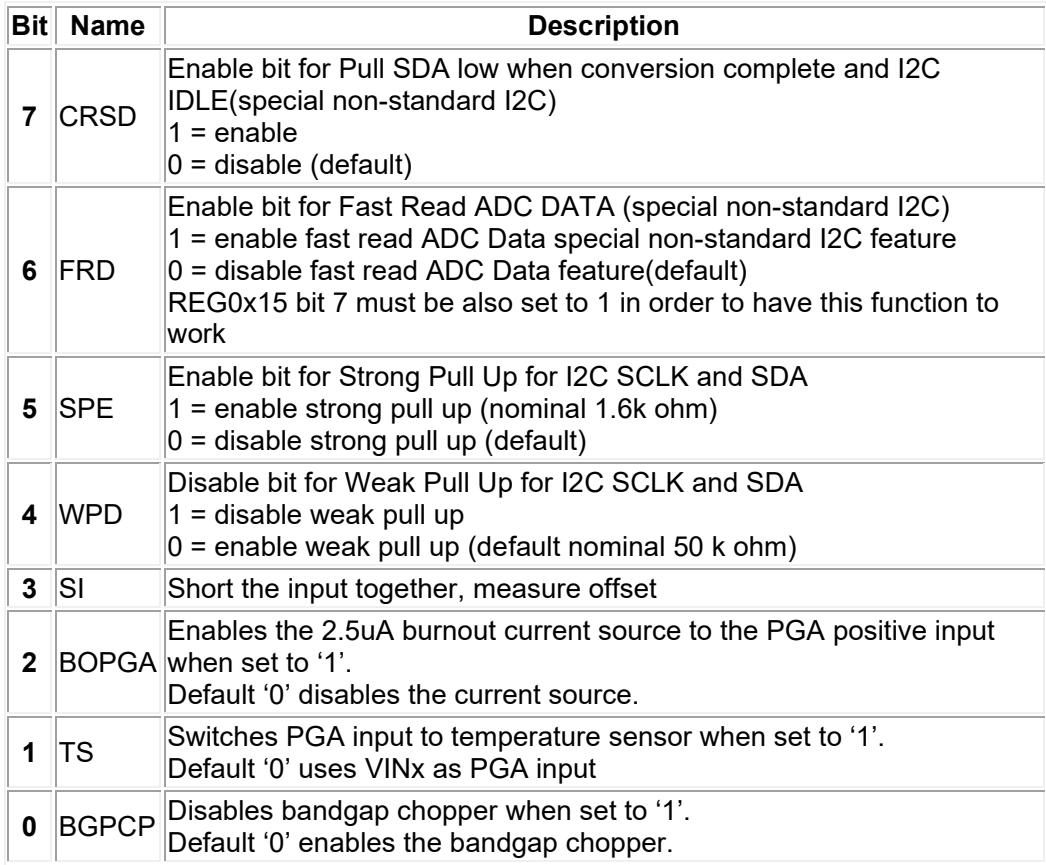
| 7 | CRSD | Enable bit for Pull SDA low when conversion complete and I2C IDLE(special non-standard I2C)1 = enable0 = disable (default) |
| 6 | FRD | Enable bit for Fast Read ADC DATA (special non-standard I2C)1 = enable fast read ADC Data special non-standard I2C feature0 = disable fast read ADC Data feature(default)REG0x15 bit 7 must be also set to 1 in order to have this function to work |
| 5 | SPE | Enable bit for Strong Pull Up for I2C SCLK and SDA1 = enable strong pull up (nominal 1.6k ohm)0 = disable strong pull up (default) |
| 4 | WPD | Disable bit for Weak Pull Up for I2C SCLK and SDA1 = disable weak pull up0 = enable weak pull up (default nominal 50 k ohm) |
| 3 | SI | Short the input together, measure offset |
| 2 | BOPGA | Enables the 2.5uA burnout current source to the PGA positive input when set to ‘1’.Default ‘0’ disables the current source. |
| 1 | TS | Switches PGA input to temperature sensor when set to ‘1’.Default ‘0’ uses VINx as PGA input |
| 0 | BGPCP | Disables bandgap chopper when set to ‘1’.Default ‘0’ enables the bandgap chopper. |
4.9 REG0x12-REG0x14: ADC Conversion Result
| REG0x12 (Read Only) | ADCO_B2 | ADC Conversion Result bit 23 to bit 16 |
| REG0x13 (Read Only) | ADCO_B1 | ADC Conversion Result bit 15 to bit 8 |
| REG0x14 (Read Only) | ADCO_B0 | ADC Conversion Result bit 7 to bit 0 |
Before reading an ADC Conversion Result, check if REG0x00 bit 5 CR=1 or DRDY pin showing Data Ready first. If not showing Data Ready, but a read of REG0x12 is performed, it will latch and shift out the previous conversion result.
There are two options are necessary read a complete 24-bit ADC conversion result: Option 1: Use "I2C Burst Read 3 bytes"
Issue I2C burst read 3-byte sequence with starting address 0x12. In read data section of this burst read sequence, continuously read 3 bytes of data, the first byte will be the bit 23 to bit 16, the second byte will be bit 15 to bit 8, the third byte will be bit 7 to bit 0 of the ADC conversion result.
Option 2: Use 3 "I2C Single Read"
Step 1: Read REG0x12: bit 23 to bit 16 ADC conversion result will be shift out
Step 2: Read REG0x13: bit 15 to bit 8 ADC conversion result will be shift out
Step 3. Read REG0x14: bit 7 to bit 0 ADC conversion result will be shift out
Note: The full 24-bit ADC conversion result is latched when the read REG0x12 command is decoded by the NAU7802. The following read of Reg0x13 and Reg0x14 will shift out the remainder of the latched ADC conversion result. This guarantees the 3 bytes of the data are from the same ADC sample conversion.
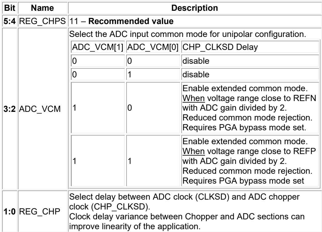
4.10REG0x15: ADC registers
| Bit | Name | Description | ||
| 5:4 | REG_CHPS | 11 – Recommended value | ||
| 3:2 | ADC_VCM | Select the ADC input common mode for unipolar configuration. | ||
| ADC_VCM[1] | ADC_VCM[0] | CHP_CLKSD Delay | ||
| 0 | 0 | disable | ||
| 0 | 1 | disable | ||
| 1 | 0 | Enable extended common mode.When voltage range close to REFN with ADC gain divided by 2.Reduced common mode rejection.Requires PGA bypass mode set. | ||
| 1 | 1 | Enable extended common mode.When voltage range close to REFP with ADC gain divided by 2.Reduced common mode rejection.Requires PGA bypass mode set | ||
| 1:0 | REG_CHP | Select delay between ADC clock (CLKSD) and ADC chopper clock (CHP_CLKSD).Clock delay variance between Chopper and ADC sections can improve linearity of the application. | ||
• Issue an I2C write REG0x15 with write data will update the ADC registers. For reading back ADC registers, make sure REG0x1B[7] RD_OTP_SEL=0 (default), then issue a I2C read REG0x15 to read ADC registers
• ADC registers and OTP[32:24] are sharing REG0x15 when read back, the REG0x1B[7] RD_OTP_SEL (default 0) is used as read select
| REG0x15 Read | REG0x1B[7]=RD_OTP_SEL=1 | Read back OTP[32:24] |
| REG0x15 Read | REG0x1B[7]=RD_OTP_SEL=0(default) | Read back ADC Registers(default) |
4.11REG0x15-REG0x17: OTP Read Value and ADC Registers Read
ADC registers and OTP[32:24] are sharing REG0x15 when read back, the REG0x1B[7] RD_OTP_SEL (default 0) is used as read select
| REG0x15 Read | REG0x1B[7]=RD_OTP_SEL=1 | Read back OTP[32:24] |
| REG0x15 Read | REG0x1B[7]=RD_OTP_SEL=0(default) | Read back ADC Registers(default) |
| REG0x16 Read | Read back OTP[23:16] | |
| REG0x17 Read | Read back OTP[15:8] |
4.12REG0x18: Read Only
4.13REG0x19: Read Only
4.14REG0x1A: Read Only
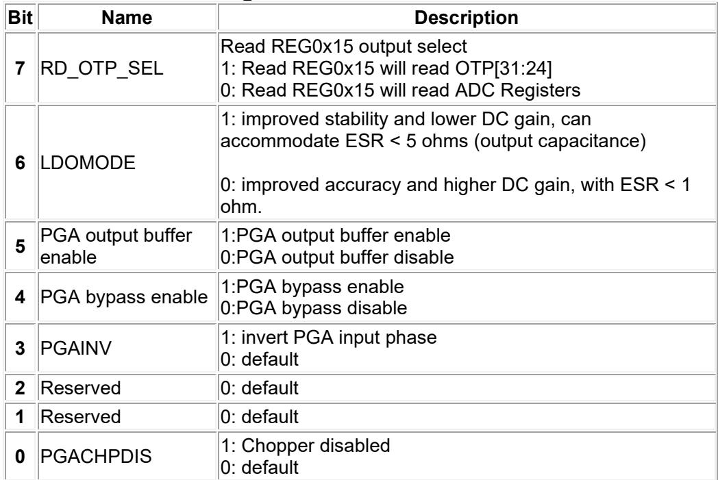
4.15REG0x1B: PGA Registers
| Bit | Name | Description |
| 7 | RD_OTP_SEL | Read REG0x15 output select1: Read REG0x15 will read OTP[31:24]0: Read REG0x15 will read ADC Registers |
| 6 | LDOMODE | 1: improved stability and lower DC gain, can accommodate ESR < 5 ohms (output capacitance)0: improved accuracy and higher DC gain, with ESR < 1 ohm. |
| 5 | PGA output buffer enable | 1:PGA output buffer enable0:PGA output buffer disable |
| 4 | PGA bypass enable | 1:PGA bypass enable0:PGA bypass disable |
| 3 | PGAINV | 1: invert PGA input phase0: default |
| 2 | Reserved | 0: default |
| 1 | Reserved | 0: default |
| 0 | PGACHPDIS | 1: Chopper disabled0: default |
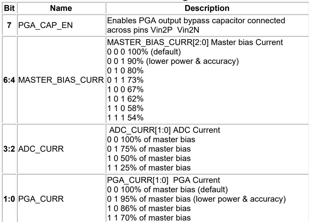
4.16REG0x1C: POWER CONTROL Register
| Bit | Name | Description |
| 7 | PGA_CAP_EN | Enables PGA output bypass capacitor connected across pins Vin2P Vin2N |
| 6:4 | MASTER_BIAS_CURR | MASTER_BIAS_CURR[2:0] Master bias Current0 0 0 100% (default)0 0 1 90% (lower power & accuracy)0 1 0 80%0 1 1 73%1 0 0 67%1 0 1 62%1 1 0 58%1 1 1 54% |
| 3:2 | ADC_CURR | ADC_CURR[1:0] ADC Current0 0 100% of master bias0 1 75% of master bias1 0 50% of master bias1 1 25% of master bias |
| 1:0 | PGA_CURR | PGA_CURR[1:0] PGA Current0 0 100% of master bias (default)0 1 95% of master bias (lower power & accuracy)1 0 86% of master bias1 1 70% of master bias |
4.17REG0x1D: Read Only
4.18REG0x1E: Read Only
4.19REG0x1F: Revision ID
| Bit | Name | Description |
| 7:4 | Reserved | MFG TEST |
| 3:0 | Revision ID | Chip Revision ID1 1 1 1 |
5 PACKAGE DIMENSIONS 5.1 SOP-16 – 150 mil
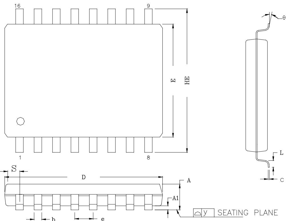
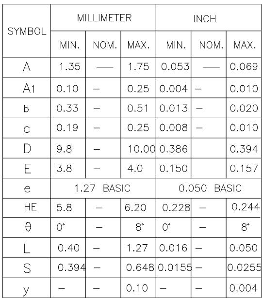
COTROL DIMENSIONS ARE IN MILLIMETERS.
| SYMBOL | MILLIMETER | INCH | ||||
| MIN. | NOM. | MAX. | MIN. | NOM. | MAX. | |
| A | 1.35 | — | 1.75 | 0.053 | — | 0.069 |
| A1 | 0.10 | — | 0.25 | 0.004 | — | 0.010 |
| b | 0.33 | — | 0.51 | 0.013 | — | 0.020 |
| c | 0.19 | — | 0.25 | 0.008 | — | 0.010 |
| D | 9.8 | — | 10.00 | 0.386 | 0.394 | |
| E | 3.8 | — | 4.0 | 0.150 | 0.157 | |
| e | 1.27 BASIC | 0.050 BASIC | ||||
| HE | 5.8 | — | 6.20 | 0.228 | — | 0.244 |
| θ | 0° | — | 8° | 0° | — | 8° |
| L | 0.40 | — | 1.27 | 0.016 | — | 0.050 |
| S | 0.394 | — | 0.648 | 0.0155 | — | 0.0255 |
| y | — | — | 0.10 | — | — | 0.004 |
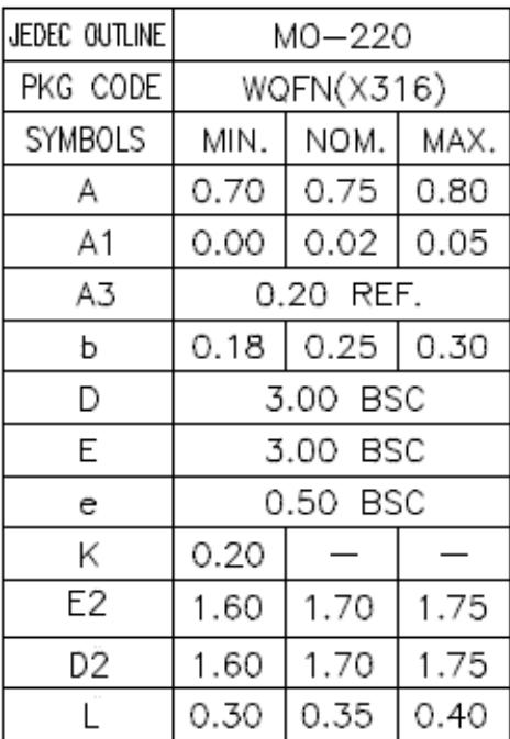
5.2 QFN-16
s
3X3 mm2, Thickness 0.8 mm(Max) ,Pitch 0.5 mm (Saw Type) EP Size 1.7X1.7mm
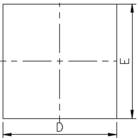
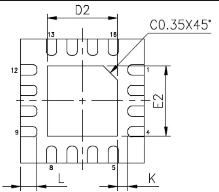
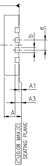
| JEDEC OUTLINE | MO-220 | ||
| PKG CODE | WQFN(X316) | ||
| SYMBOLS | MIN. | NOM. | MAX. |
| A | 0.70 | 0.75 | 0.80 |
| A1 | 0.00 | 0.02 | 0.05 |
| A3 | 0.20 REF. | ||
| b | 0.18 | 0.25 | 0.30 |
| D | 3.00 BSC | ||
| E | 3.00 BSC | ||
| e | 0.50 BSC | ||
| K | 0.20 | — | — |
| E2 | 1.60 | 1.70 | 1.75 |
| D2 | 1.60 | 1.70 | 1.75 |
| L | 0.30 | 0.35 | 0.40 |
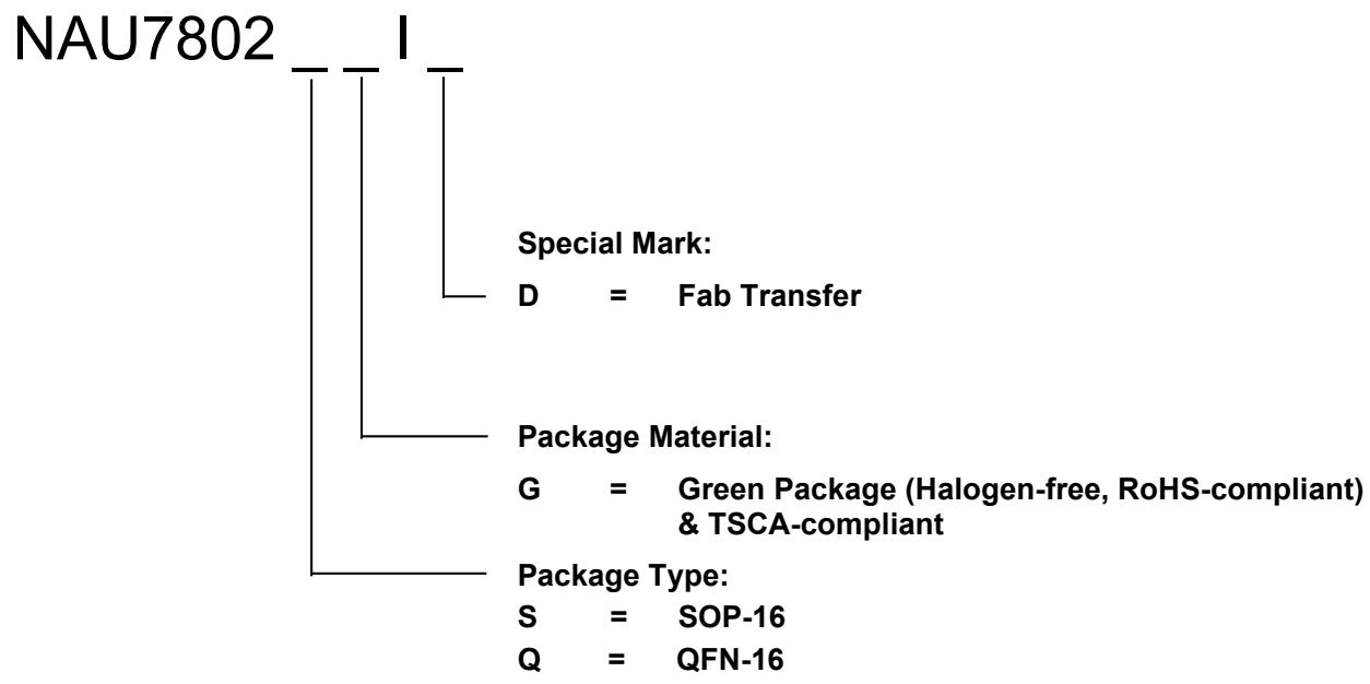
6 ORDERING INFORMATION
| Part Number | Dimension | Package | Package Material |
| NAU7802SGI | 10x4 mm | SOP-16 | Green |
| NAU7802SGID | 10x4 mm | SOP-16 | Green |
| NAU7802QGI | 3x3 mm | QFN-16 | Green |
| NAU7802QGID | 3x3 mm | QFN-16 | Green |
7 REVISION HISTORY
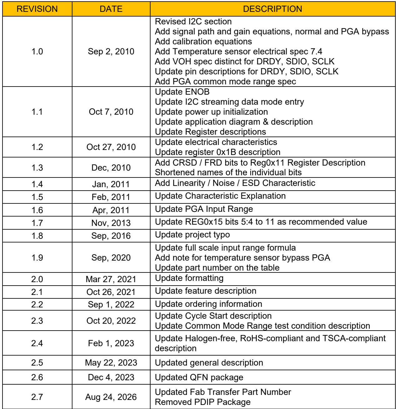
| REVISION | DATE | DESCRIPTION |
| 1.0 | Sep 2, 2010 | Revised I2C sectionAdd signal path and gain equations, normal and PGA bypassAdd calibration equationsAdd Temperature sensor electrical spec 7.4Add VOH spec distinct for DRDY, SDIO, SCLKUpdate pin descriptions for DRDY, SDIO, SCLKAdd PGA common mode range spec |
| 1.1 | Oct 7, 2010 | Update ENOBUpdate I2C streaming data mode entryUpdate power up initializationUpdate application diagram & descriptionUpdate Register descriptions |
| 1.2 | Oct 27, 2010 | Update electrical characteristicsUpdate register 0x1B description |
| 1.3 | Dec, 2010 | Add CRSD / FRD bits to Reg0x11 Register DescriptionShortened names of the individual bits |
| 1.4 | Jan, 2011 | Add Linearity / Noise / ESD Characteristic |
| 1.5 | Feb, 2011 | Update Characteristic Explanation |
| 1.6 | Apr, 2011 | Update PGA Input Range |
| 1.7 | Nov, 2013 | Update REG0x15 bits 5:4 to 11 as recommended value |
| 1.8 | Sep, 2016 | Update project typo |
| 1.9 | Sep, 2020 | Update full scale input range formulaAdd note for temperature sensor bypass PGAUpdate part number on the table |
| 2.0 | Mar 27, 2021 | Update formatting |
| 2.1 | Oct 26, 2021 | Update feature description |
| 2.2 | Sep 1, 2022 | Update ordering information |
| 2.3 | Oct 20, 2022 | Update Cycle Start descriptionUpdate Common Mode Range test condition description |
| 2.4 | Feb 1, 2023 | Update Halogen-free, RoHS-compliant and TSCA-compliant description |
| 2.5 | May 22, 2023 | Updated general description |
| 2.6 | Dec 4, 2023 | Updated QFN package |
| 2.7 | Aug 24, 2026 | Updated Fab Transfer Part NumberRemoved PDIP Package |
Figures and diagrams from the PDF
Preview the extracted datasheet assets and open any image in a separate tab for closer inspection.














Use this datasheet from any agent
Send the page, markdown, chunks, or search endpoint to ChatGPT, Claude, embedr-app, or your own tooling.