
ICM-42688-P 6-Axis IMU
TDK InvenSense ICM-42688-P high-precision 6-axis MEMS MotionTracking IMU with 3-axis gyroscope, 3-axis accelerometer, I3C/I2C/SPI host interface, 2 kB FIFO, programmable interrupts, and 14-pin 2.5 x 3.0 mm LGA package.
High Precision 6-Axis MEMS MotionTrackingTM Device
ICM-42688-P HIGHLIGHTS
The ICM-42688-P is a 6-axis MEMS MotionTracking device that combines a 3-axis gyroscope and a 3-axis accelerometer. It has a configurable host interface that supports I3CSM, I2C and SPI serial communication, features a 2 kB FIFO and 2 programmable interrupts with ultra-low-power wake-on-motion support to minimize system power consumption.
ICM-42688-P supports highly accurate external clock input, that helps to reduce system level sensitivity error, improve orientation measurement from gyroscope data, reduce ODR sensitivity to temperature and device to device variation.
The device includes industry first 20-bits data format support in FIFO for high-data resolution. This FIFO format encapsulates 19-bits of gyroscope data and 18- bits of accelerometer data.
Other industry-leading features include InvenSense on-chip APEX Motion Processing engine for gesture recognition, activity classification, and pedometer, along with programmable digital filters, and an embedded temperature sensor.
The device supports a VDD operating range of 1.71V to 3.6V, and a separate digital IO supply, VDDIO from 1.71V to 3.6V.
ICM-42688-P FEATURES
Gyroscope Noise: 2.8 mdps/Hz & Accelerometer Noise: 70 µg/Hz
Low-Noise mode 6-axis current consumption of 0.88 mA
User selectable Gyro Full-scale range (dps): ± 15.6/31.2/62.5/125/250/500/1000/2000
User selectable Accelerometer Full-scale range (g): ± 2/4/8/16
User-programmable digital filters for gyro, accel, and temp sensor
• APEX Motion Functions:
o Pedometer, Tilt Detection, Tap Detection
o Wake on Motion, Significant Motion Detection
Host interface: 12.5 MHz I3CSM, 1 MHz I2C, 24 MHz SPI
APPLICATIONS
• AR/VR Controllers
• Head Mounted Displays
• Wearables
• Sports
• Robotics
• IoT Applications
BLOCK DIAGRAM
| AP/MCU | I3C $^{SM}$ /I2C/SPI | ICM-42688-P |
| INT1 | ||
| INT2 |
ORDERING INFORMATION
| PART | TEMP RANGE | PACKAGE |
| ICM-42688-P† | -40°C to +85°C | 2.5x3mm 14-Pin LGA |
†Denotes RoHS and Green-Compliant Package
TDK-INVENSENSE SENSORS FOR SMARTPHONE, MOBILE & IOT APPLICATIONS
| Parameter | ICM-40607 Sensorhub | ICM-42605 Sensorhub | ICM-42686-P Handheld Action | ICM-42688-P HMD & Robotics |
| GYRO Noise (mdps/rt-Hz) | 7 | 3.8 | 5.3 | 2.8 |
| GYRO Offset Temp Stability (mdps/°C) | ±30 | ±20 | ±10 | ±5 |
| GYRO Range & Resolution | ±2000dps; 16-bits | ±2000dps; 16-bits | ±4000dps; 16/19-bits | ±2000dps; 16/19-bits |
| ACCEL Noise (μg/rt-Hz) | 110 | 70 | 70 | AXY: 65; AZ: 70 |
| ACCEL Range & Resolution | ±16g; 16-bits | ±16g; 16-bits | ±32g; 16/18-bits | ±16g; 16/18-bits |
| ODR & Sample Synch | 8kHz; No RTC | 8kHz; No RTC | 32kHz; RTC | 32kHz; RTC |
TABLE OF CONTENTS
ICM-42688-P Highlights .... 1
Block Diagram .... 1
ICM-42688-P Features .... 1
Applications .... 1
Ordering Information .... 1
TDK-Invensense Sensors for Smartphone, Mobile & IoT Applications .... 1
Table of Figures.... 8
Table of Tables.... 8
1 Introduction.... 9
1.1 Purpose and Scope.... 9
1.2 Product Overview.... 9
1.3 Applications.... 9
2 Features.... 10
2.1 Gyroscope Features.... 10
2.2 Accelerometer Features.... 10
2.3 Motion Features.... 10
2.4 Additional Features.... 10
3 Electrical Characteristics.... 11
3.1 Gyroscope Specifications.... 11
3.2 Accelerometer Specifications.... 12
3.3 Electrical Specifications.... 13
3.4 I²C Timing Characterization.... 15
3.5 SPI Timing Characterization – 4-Wire SPI Mode.... 16
3.6 SPI Timing Characterization – 3-Wire SPI Mode.... 17
3.7 RTC (CLKIN) Timing Characterization.... 18
3.8 Absolute Maximum Ratings.... 19
4 Applications Information.... 20
4.1 Pin Out Diagram and Signal Description.... 20
4.2 Typical Operating Circuit.... 21
4.3 Bill of Materials for External Components.... 22
4.4 System Block Diagram.... 23
4.5 Overview.... 23
4.6 Three-Axis MEMS Gyroscope with 16-bit ADCs and Signal Conditioning.... 23
4.7 Three-Axis MEMS Accelerometer with 16-bit ADCs and Signal Conditioning.... 23
4.8 I3C $^{SM}$ , I²C and SPI Host Interface.... 23
4.9 Self-Test.... 23
4.10 Clocking.... 24
4.11 Sensor Data Registers 24
4.12 Interrupts 24
4.13 Digital-Output Temperature Sensor 25
4.14 Bias and LDOs 25
4.15 Charge Pump 25
4.16 Standard Power Modes 25
5 Signal Path 26
5.1 Summary of Parameters Used to Configure the Signal Path 26
5.2 Notch Filter 26
5.3 Anti-Alias Filter 28
5.4 User Programmable Offset 30
5.5 UI Filter Block 30
5.6 UI Path ODR And FSR Selection 34
6 FIFO 37
6.1 Packet Structure 37
6.2 FIFO Header 39
6.3 Maximum FIFO Storage 40
6.4 FIFO Configuration Registers 40
7 Programmable Interrupts 42
8 APEX Motion Functions 43
8.1 APEX ODR Support 43
8.2 DMP Power Save Mode 44
8.3 Pedometer Programming 44
8.4 Tilt Detection Programming 45
8.5 Tap Detection Programming 45
8.6 Wake on Motion Programming 46
8.7 Significant Motion Detection Programming 47
9 Digital Interface 48
9.1 I3C $^{SM}$ , I $^{2}$ C and SPI Serial Interfaces 48
9.2 I3C $^{SM}$ Interface 48
9.3 I $^{2}$ C Interface 48
9.4 I $^{2}$ C Communications Protocol 48
9.5 I $^{2}$ C Terms 50
9.6 SPI Interface 52
10 Assembly 53
10.1 Orientation of Axes 53
10.2 Package Dimensions 54
11 Part Number Package Marking 56
12 Use Notes 57
12.1 Accelerometer Mode Transitions 57
12.2 Accelerometer Low Power (LP) Mode Averaging Filter Setting....57
12.3 Settings for I²C, I3CSM, and SPI Operation....57
12.4 Notch Filter and Anti-Alias Filter Operation....57
12.5 External Clock Input Effect on ODR....57
12.6 INT_ASYNC_RESET Configuration....58
12.7 FIFO Timestamp Interval Scaling....58
12.8 Supplementary Information for FIFO_HOLD_LAST_DATA_EN....58
12.9 Register Values Modification....59
3 Register Map....60
13.1 User Bank 0 Register Map....60
13.2 User Bank 1 Register Map....61
13.3 User Bank 2 Register Map....62
13.4 User Bank 3 Register Map....62
13.5 User Bank 4 Register Map....62
4 User Bank 0 Register Map – Descriptions....64
14.1 DEVICE_CONFIG....64
14.2 DRIVE_CONFIG....64
14.3 INT_CONFIG....65
14.4 FIFO_CONFIG....65
14.5 TEMP_DATA1....65
14.6 TEMP_DATA0....66
14.7 ACCEL_DATA_X1....66
14.8 ACCEL_DATA_X0....66
14.9 ACCEL_DATA_Y1....66
14.10 ACCEL_DATA_Y0....67
14.11 ACCEL_DATA_Z1....67
14.12 ACCEL_DATA_Z0....67
14.13 GYRO_DATA_X1....67
14.14 GYRO_DATA_X0....67
14.15 GYRO_DATA_Y1....68
14.16 GYRO_DATA_Y0....68
14.17 GYRO_DATA_Z1....68
14.18 GYRO_DATA_Z0....68
14.19 TMST_FSYNCH....68
14.20 TMST_FSYNCL....69
14.21 INT_STATUS....69
14.22 FIFO_COUNTH....69
14.23 FIFO_COUNTL....70
14.24 FIFO_DATA....70
14.25 APEX_DATA0....70
14.26 APEX_DATA1....70
14.27 APEX_DATA2....71
14.28 APEX_DATA3....71
14.29 APEX_DATA4....72
14.30 APEX_DATA5....72
14.31 INT_STATUS2....73
14.32 INT_STATUS3....73
14.33 SIGNAL_PATH_RESET....73
14.34 INTF_CONFIG0....74
14.35 INTF_CONFIG1....75
14.36 PWR_MGMT0....76
14.37 GYRO_CONFIG0....77
14.38 ACCEL_CONFIG0....78
14.39 GYRO_CONFIG1....79
14.40 GYRO_ACCEL_CONFIG0....80
14.41 ACCEL_CONFIG1....81
14.42 TMST_CONFIG....81
14.43 APEX_CONFIG0....82
14.44 SMD_CONFIG....82
14.45 FIFO_CONFIG1....83
14.46 FIFO_CONFIG2....83
14.47 FIFO_CONFIG3....83
14.48 FSYNC_CONFIG....84
14.49 INT_CONFIG0....84
14.50 INT_CONFIG1....85
14.51 INT_SOURCE0....85
14.52 INT_SOURCE1....86
14.53 INT_SOURCE3....86
14.54 INT_SOURCE4....87
14.55 FIFO_LOST_PKT0....87
14.56 FIFO_LOST_PKT1....87
14.57 SELF_TEST_CONFIG....88
14.58 WHO_AM_I....88
14.59 REG_BANK_SEL....88
User Bank 1 Register Map – Descriptions....89
15.1 SENSOR_CONFIG0....89
15.2 GYRO_CONFIG_STATIC2....89
15.3 GYRO_CONFIG_STATIC3....89
15.4 GYRO_CONFIG_STATIC4....90
15.5 GYRO_CONFIG_STATIC5....90
15.6 GYRO_CONFIG_STATIC6....90
15.7 GYRO_CONFIG_STATIC7....90
15.8 GYRO_CONFIG_STATIC8....91
15.9 GYRO_CONFIG_STATIC9....91
15.10 GYRO_CONFIG_STATIC10....91
15.11 XG_ST_DATA....92
15.12 YG_ST_DATA....92
15.13 ZG_ST_DATA....92
15.14 TMSTVAL0....92
15.15 TMSTVAL1....93
15.16 TMSTVAL2....93
15.17 INTF_CONFIG4....93
15.18 INTF_CONFIG5....94
15.19 INTF_CONFIG6....94
16 User Bank 2 Register Map – Descriptions....95
16.1 ACCEL_CONFIG_STATIC2....95
16.2 ACCEL_CONFIG_STATIC3....95
16.3 ACCEL_CONFIG_STATIC4....95
16.4 XA_ST_DATA....95
16.5 YA_ST_DATA....96
16.6 ZA_ST_DATA....96
17 User Bank 3 Register Map – Descriptions....97
17.1 CLKDIV....97
18 User Bank 4 Register Map – Descriptions....98
18.1 APEX_CONFIG1....98
18.2 APEX_CONFIG2....99
18.3 APEX_CONFIG3....100
18.4 APEX_CONFIG4....101
18.5 APEX_CONFIG7....101
18.6 APEX_CONFIG8....101
18.7 APEX_CONFIG9....102
18.8 ACCEL_WOM_X_THR....102
18.9 ACCEL_WOM_Y_THR....102
18.10 ACCEL_WOM_Z_THR....102
18.11 INT_SOURCE6....103
18.12 INT_SOURCE7....103
18.13 INT_SOURCE8....104
18.14 INT_SOURCE9....104
18.15 INT_SOURCE10....105
18.16 OFFSET_USER0....105
18.17 OFFSET_USER1....105
18.18 OFFSET_USER2....105
18.19 OFFSET_USER3....106
18.20 OFFSET_USER4....106
18.21 OFFSET_USER5....106
18.22 OFFSET_USER6....106
18.23 OFFSET_USER7....107
18.24 OFFSET_USER8....107
19 Reference....108
20 Document Information....109
20.1 Revision History....109
TABLE OF FIGURES
Figure 1. I²C Bus Timing Diagram ..... 15
Figure 2. 4-Wire SPI Bus Timing Diagram ..... 16
Figure 3. 3-Wire SPI Bus Timing Diagram ..... 17
Figure 4. RTC Timing Diagram ..... 18
Figure 5. Pin Out Diagram for ICM-42688-P 2.5x3.0x0.91 mm LGA ..... 20
Figure 6. ICM-42688-P Application Schematic (I3C $^{SM}$ / I²C Interface to Host) ..... 21
Figure 7. ICM-42688-P Application Schematic (SPI Interface to Host) ..... 21
Figure 8. ICM-42688-P System Block Diagram ..... 23
Figure 9. ICM-42688-P Signal Path ..... 26
Figure 10. FIFO Packet Structure ..... 37
Figure 11. Maximum FIFO Storage ..... 40
Figure 12. START and STOP Conditions ..... 49
Figure 13. Acknowledge on the I²C Bus ..... 49
Figure 14. Complete I²C Data Transfer ..... 50
Figure 15. Typical SPI Master/Slave Configuration ..... 52
Figure 16. Orientation of Axes of Sensitivity and Polarity of Rotation ..... 53
TABLE OF TABLES
Table 1. Gyroscope Specifications ..... 11
Table 2. Accelerometer Specifications ..... 12
Table 3. D.C. Electrical Characteristics ..... 13
Table 4. A.C. Electrical Characteristics ..... 14
Table 5. I²C Timing Characteristics ..... 15
Table 6. 4-Wire SPI Timing Characteristics (24-MHz Operation) ..... 16
Table 7. 3-Wire SPI Timing Characteristics (24-MHz Operation) ..... 17
Table 8. RTC Timing Characteristics ..... 18
Table 9. Absolute Maximum Ratings ..... 19
Table 10. Signal Descriptions ..... 20
Table 11. Bill of Materials ..... 22
Table 12. Standard Power Modes for ICM-42688-P ..... 25
Table 13. I²C Terms ..... 51
1 INTRODUCTION
1.1 PURPOSE AND SCOPE
This document is a product specification, providing a description, specifications, and design related information on the ICM-42688-P Single-Interface MotionTracking device. The device is housed in a small 2.5x3x0.91 mm 14-pin LGA package.
1.2 PRODUCT OVERVIEW
The ICM-42688-P is a 6-axis MotionTracking device that combines a 3-axis gyroscope, and a 3-axis accelerometer in a smal 2.5x3x0.91 mm (14-pin LGA) package. It also features a 2K-byte FIFO that can lower the traffic on the serial bus interface, and reduce power consumption by allowing the system processor to burst read sensor data and then go into a low-power mode. ICM-42688-P, with its 6-axis integration, enables manufacturers to eliminate the costly and complex selection, qualification, and system level integration of discrete devices, guaranteeing optimal motion performance for consumers.
The gyroscope supports eight programmable full-scale range settings from ±15.625dps to ±2000dps, and the accelerometer supports four programmable full-scale range settings from ±2g to ±16g.
ICM-42688-P also supports external clock input for highly accurate 31kHz to 50kHz clock, that helps to reduce system level sensitivity error, improve orientation measurement from gyroscope data, reduce ODR sensitivity to temperature and device to device variation.
The device includes industry first 20-bits data format support in FIFO for high-data resolution. This FIFO format encapsulates 19-bits of gyroscope data and 18-bits of accelerometer data for high precision applications. Other industry-leading features include on-chip 16-bit ADCs, programmable digital filters, an embedded temperature sensor, and programmable interrupts. The device features I3CSM, I2C and SPI serial interfaces, a VDD operating range of 1.71 V to 3.6 V, and a separate VDDIO operating range of 1.71 V to 3.6 V.
The host interface can be configured to support I3CSM slave, I2C slave, or SPI slave modes. The I3CSM interface supports speeds up to 12.5MHz (data rates up to 12.5Mbps in SDR mode, 25Mbps in DDR mode), the I2C interface supports speeds up to 1 MHz, and the SPI interface supports speeds up to 24 MHz.
By leveraging its patented and volume-proven CMOS-MEMS fabrication platform, which integrates MEMS wafers with companion CMOS electronics through wafer-level bonding, InvenSense has driven the package size down to a footprint and thickness of 2.5x3x0.91 mm (14-pin LGA), to provide a very small yet high performance low cost package. The device provides high robustness by supporting 20,000g shock reliability.
1.3 APPLICATIONS
• AR/VR Controllers
• Head Mounted Displays
Wearables
• Sports
• Robotics
2 FEATURES
2.1 GYROSCOPE FEATURES
The triple-axis MEMS gyroscope in the ICM-42688-P includes a wide range of features:
● Digital-output X-, Y-, and Z-axis angular rate sensors (gyroscopes) with programmable full-scale range of ±15.625, ±31.25, ±62.5, ±125, ±250, ±500, ±1000, and ±2000 degrees/sec
• Low Noise (LN) power mode support
• Digitally-programmable low-pass filters
• Factory calibrated sensitivity scale factor
• Self-test
2.2 ACCELEROMETER FEATURES
The triple-axis MEMS accelerometer in ICM-42688-P includes a wide range of features:
• Digital-output X-, Y-, and Z-axis accelerometer with programmable full-scale range of ±2g, ±4g ±8g and ±16g
Low Noise (LN) and Low Power (LP) power modes support
• User-programmable interrupts
• Wake-on-motion interrupt for low power operation of applications processor
Self-test
2.3 MOTION FEATURES
ICM-42688-P includes the following motion features, also known as APEX (Advanced Pedometer and Event Detection – neXt gen)
Pedometer: Tracks Step Count, also issues Step Detect interrupt
• Tilt Detection: Issues an interrupt when the Tilt angle exceeds 35 for more than a programmable time
• Tap Detection: Issues an interrupt when a tap is detected, along with the tap count
• Wake on Motion: Detects motion when accelerometer data exceeds a programmable threshold
• Significant Motion Detection: Detects Significant Motion if Wake on Motion events are detected during a programmable time window
2.4 ADDITIONAL FEATURES
ICM-42688-P includes the following additional features:
External clock input supports highly accurate clock input from 31kHz to 50kHz, helps to reduce system level sensitivity error, improve orientation measurement from gyroscope data, reduce ODR sensitivity to temperature and device to device variation
• 2K byte FIFO buffer enables the applications processor to read the data in bursts
20-bits data format support in FIFO for high-data resolution
• User-programmable digital filters for gyroscope, accelerometer, and temperature sensor
• 12.5MHz I3CSM (data rates up to 12.5Mbps in SDR mode, 25Mbps in DDR mode) / 1 MHz I2C / 24 MHz SPI slave host interface
• Digital-output temperature sensor
• Smallest and thinnest LGA package for portable devices: 2.5x3x0.91 mm (14-pin LGA)
• 20,000 g shock tolerant
MEMS structure hermetically sealed and bonded at wafer level
RoHS and Green compliant
3 ELECTRICAL CHARACTERISTICS
3.1 GYROSCOPE SPECIFICATIONS
Typical Operating Circuit of section 4.2, VDD = 1.8 V, VDDIO = 1.8 V, ${ \mathsf { T } } _ { \mathsf { A } } { = } 2 5 ^ { \circ } { \mathsf { C } } ,$ unless otherwise noted.
| PARAMETER | CONDITIONS | MIN | TYP | MAX | UNITS | NOTES |
| GYROSCOPE SENSITIVITY | ||||||
| Full-Scale Range | GYRO_FS_SEL=0 | ±2000 | o/s | 2 | ||
| GYRO_FS_SEL =1 | ±1000 | o/s | 2 | |||
| GYRO_FS_SEL =2 | ±500 | o/s | 2 | |||
| GYRO_FS_SEL =3 | ±250 | o/s | 2 | |||
| GYRO_FS_SEL =4 | ±125 | o/s | 2 | |||
| GYRO_FS_SEL =5 | ±62.5 | o/s | 2 | |||
| GYRO_FS_SEL =6 | ±31.25 | o/s | 2 | |||
| GYRO_FS_SEL =7 | ±15.625 | o/s | 2 | |||
| Gyroscope ADC Word Length | Output in two's complement format | 16 | bits | 2, 5 | ||
| Sensitivity Scale Factor | GYRO_FS_SEL=0 | 16.4 | LSB/(o/s) | 2 | ||
| GYRO_FS_SEL =1 | 32.8 | LSB/(o/s) | 2 | |||
| GYRO_FS_SEL =2 | 65.5 | LSB/(o/s) | 2 | |||
| GYRO_FS_SEL =3 | 131 | LSB/(o/s) | 2 | |||
| GYRO_FS_SEL =4 | 262 | LSB/(o/s) | 2 | |||
| GYRO_FS_SEL =5 | 524.3 | LSB/(o/s) | 2 | |||
| GYRO_FS_SEL =6 | 1048.6 | LSB/(o/s) | 2 | |||
| GYRO_FS_SEL =7 | 2097.2 | LSB/(o/s) | 2 | |||
| Sensitivity Scale Factor Initial Tolerance | Component and Board-level, 25°C | ±0.5 | % | 1 | ||
| Sensitivity Scale Factor Variation Over Temperature | 0°C to +70°C | ±0.005 | %/°C | 3 | ||
| Nonlinearity | Best fit straight line; 25°C | ±0.1 | % | 3 | ||
| Cross-Axis Sensitivity | Board-level | ±1.25 | % | 3 | ||
| ZERO-RATE OUTPUT (ZRO) | ||||||
| Initial ZRO Tolerance | Board-level, 25°C | ±0.5 | o/s | 3 | ||
| ZRO Variation vs. Temperature | 0°C to +70°C | ±0.005 | o/s/°C | 3 | ||
| OTHER PARAMETERS | ||||||
| Rate Noise Spectral Density | @ 10 Hz | 0.0028 | o/s /VHz | 1 | ||
| Total RMS Noise | Bandwidth = 100 Hz | 0.028 | o/s-rms | 4 | ||
| Gyroscope Mechanical Frequencies | 25 | 27 | 29 | KHz | 1 | |
| Low Pass Filter Response | ODR < 1kHz | 5 | 500 | Hz | 2 | |
| ODR ≥ 1kHz | 42 | 3979 | Hz | 2 | ||
| Gyroscope Start-Up Time | Time from gyro enable to gyro drive ready | 30 | ms | 3 | ||
| Output Data Rate | 12.5 | 32000 | Hz | 2 | ||
Table 1. Gyroscope Specifications
Notes:
- Tested in production.
- Guaranteed by design.
- Derived from validation or characterization of parts, not tested in production.
- Calculated from Rate Noise Spectral Density.
- 20-bits data format supported in FIFO, see section 6.1.
3.2 ACCELEROMETER SPECIFICATIONS
Typical Operating Circuit of section 4.2, VDD = 1.8 V, VDDIO = 1.8 V, TA=25°C, unless otherwise noted.
| PARAMETER | CONDITIONS | MIN | TYP | MAX | UNITS | NOTES | |
| ACCELEROMETER SENSITIVITY | |||||||
| Full-Scale Range | ACCEL_FS_SEL =0 | ±16 | g | 2 | |||
| ACCEL_FS_SEL =1 | ±8 | g | 2 | ||||
| ACCEL_FS_SEL =2 | ±4 | g | 2 | ||||
| ACCEL_FS_SEL =3 | ±2 | g | 2 | ||||
| ADC Word Length | Output in two's complement format | 16 | bits | 2,5 | |||
| Sensitivity Scale Factor | ACCEL_FS_SEL =0 | 2,048 | LSB/g | 2 | |||
| ACCEL_FS_SEL =1 | 4,096 | LSB/g | 2 | ||||
| ACCEL_FS_SEL =2 | 8,192 | LSB/g | 2 | ||||
| ACCEL_FS_SEL =3 | 16,384 | LSB/g | 2 | ||||
| Sensitivity Scale Factor Initial Tolerance | Component and Board-level, 25°C | ±0.5 | % | 1 | |||
| Sensitivity Change vs. Temperature | -40°C to +85°C | ±0.005 | %/°C | 3 | |||
| Nonlinearity | Best Fit Straight Line, ±2g | ±0.1 | % | 3 | |||
| Cross-Axis Sensitivity | Board-level | ±1 | % | 3 | |||
| ZERO-G OUTPUT | |||||||
| Initial Tolerance | Board-level, all axes | ±20 | mg | 3 | |||
| Zero-G Level Change vs. Temperature | -40°C to +85°C | ±0.15 | mg/°C | 3 | |||
| OTHER PARAMETERS | |||||||
| Power Spectral Density | @ 10 Hz | X and Y-axis | 65 | μg/VHz | 1 | ||
| Z-axis | 70 | μg/VHz | 1 | ||||
| RMS Noise | Bandwidth = 100 Hz | X and Y-axis | 0.65 | mg-rms | 4 | ||
| Z-axis | 0.70 | mg-rms | 4 | ||||
| Low-Pass Filter Response | ODR < 1kHz | 5 | 500 | Hz | 2 | ||
| ODR ≥ 1kHz | 42 | 3979 | Hz | 2 | |||
| Accelerometer Startup Time | From sleep mode to valid data | 10 | ms | 3 | |||
| Output Data Rate | 1.5625 | 32000 | Hz | 2 | |||
Table 2. Accelerometer Specifications
Notes:
Tested in production.
Guaranteed by design.
Derived from validation or characterization of parts, not tested in production.
Calculated from Power Spectral Density.
20-bits data format supported in FIFO, see section 6.1.
3.3 ELECTRICAL SPECIFICATIONS
3.3.1 D.C. Electrical Characteristics
Typical Operating Circuit of section 4.2, VDD = 1.8 V, VDDIO = 1.8 V, ${ \mathsf { T } } _ { \mathsf { A } } { = } 2 5 ^ { \circ } { \mathsf { C } } ,$ unless otherwise noted.
| PARAMETER | CONDITIONS | MIN | TYP | MAX | UNITS | NOTES |
| SUPPLY VOLTAGES | ||||||
| VDD | 1.71 | 1.8 | 3.6 | V | 1 | |
| VDDIO | 1.71 | 1.8 | 3.6 | V | 1 | |
| SUPPLY CURRENTS | ||||||
| Low-Noise Mode | 6-Axis Gyroscope + Accelerometer | 0.88 | mA | 2 | ||
| 3-Axis Accelerometer | 0.28 | mA | 2 | |||
| 3-Axis Gyroscope | 0.73 | mA | 2 | |||
| Full-Chip Sleep Mode | At 25°C | 7.5 | μA | 2 | ||
| TEMPERATURE RANGE | ||||||
| Specified Temperature Range | Performance parameters are not applicable beyond Specified Temperature Range | -40 | +85 | °C | 1 | |
Table 3. D.C. Electrical Characteristics
Notes:
Guaranteed by design.
Derived from validation or characterization of parts, not tested in production.
3.3.2 A.C. Electrical Characteristics
Typical Operating Circuit of section 4.2, VDD = 1.8 V, VDDIO = 1.8 V, TA=25°C, unless otherwise noted.
| PARAMETER | CONDITIONS | MIN | TYP | MAX | UNITS | NOTES |
| SUPPLIES | ||||||
| Supply Ramp Time | Monotonic ramp. Ramp rate is 10% to 90% of the final value | 0.01 | 3 | ms | 1 | |
| Power Supply Noise | 10 | mV peak-peak | 1 | |||
| TEMPERATURE SENSOR | ||||||
| Operating Range | Ambient | -40 | 85 | °C | 1 | |
| 25°C Output | 0 | LSB | 3 | |||
| ADC Resolution | Output in two's complement format | 16 | bits | 2 | ||
| ODR | With Filter | 25 | 8000 | Hz | 2 | |
| Room Temperature Offset | 25°C | -5 | 5 | °C | 3 | |
| Stabilization Time | 14000 | μs | 2 | |||
| Sensitivity | Untrimmed | 132.48 | LSB/°C | 1 | ||
| Sensitivity for FIFO data | 2.07 | LSB/°C | 1 | |||
| POWER-ON RESET | ||||||
| Start-up time for register read/write | From power-up | 1 | ms | 1 | ||
| I2C ADDRESS | ||||||
| I2C ADDRESS | AP_AD0 = 0AP_AD0 = 1 | 11010001101001 | ||||
| DIGITAL INPUTS (FSYNC, SCLK, SDI, CS) | ||||||
| VIH, High Level Input Voltage | 0.7*VDDIO | V | 1 | |||
| VIL, Low Level Input Voltage | 0.3*VDDIO | V | ||||
| CI, Input Capacitance | < 10 | pF | ||||
| DIGITAL OUTPUT (SDO, INT1, INT2) | ||||||
| VOH, High Level Output Voltage | RLOAD=1 MΩ; | 0.9*VDDIO | V | 1 | ||
| VOLL, LOW-Level Output Voltage | RLOAD=1 MΩ; | 0.1*VDDIO | V | |||
| VOLINT, INT Low-Level Output Voltage | OPEN=1, 0.3 mA sinkCurrent | 0.1 | V | |||
| Output Leakage Current | OPEN=1 | 100 | nA | |||
| tINT, INT Pulse Width | int_tpulse_duration= 0 , 1 (100us, 8us ) ; | 8 | 100 | μs | ||
| I2C I/O (SCL, SDA) | ||||||
| VIL, LOW-Level Input Voltage | -0.5 V | 0.3*VDDIO | V | 1 | ||
| VIH, HIGH-Level Input Voltage | 0.7*VDDIO | VDDIO + 0.5 V | V | |||
| Vhys, Hysteresis | 0.1*VDDIO | V | ||||
| VOL, LOW-Level Output Voltage | 3 mA sink current | 0 | 0.4 | V | ||
| IOL, LOW-Level Output Current | VOL=0.4 VVOL=0.6 V | 36 | mAmA | |||
| Output Leakage Current | 100 | nA | ||||
| tof, Output Fall Time from VIHmax to VILmax | Cb bus capacitance in pf | 20+0.1Cb | 300 | ns | ||
| INTERNAL CLOCK SOURCE | ||||||
| Clock Frequency Initial Tolerance | CLKSEL='2b00 or gyro inactive; 25°C | -3 | +3 | % | 1 | |
| CLK_SEL='2b01 and gyro active; 25°C | -1.5 | +1.5 | % | 1 | ||
| Frequency Variation over Temperature | CLK_SEL='2b00 or gyro inactive; -40°C to +85°C | ±3 | % | 1 | ||
| CLK_SEL='2b01 and gyro active; -40°C to +85°C | ±2 | % | 1 | |||
| EXTERNAL CLOCK SOURCE | ||||||
| Clock Frequency | 31 | 32 | 50 | kHz | 1 | |
Table 4. A.C. Electrical Characteristics
Notes:
- Based on characterization. Not tested in production.
- Guaranteed by design.
- Production tested.
3.4 I2C TIMING CHARACTERIZATION
Typical Operating Circuit of section 4.2, VDD = 1.8 V, VDDIO = 1.8 V, ${ \mathsf { T } } _ { \mathsf { A } } { = } 2 5 ^ { \circ } { \mathsf { C } } ,$ unless otherwise noted.
| Parameters | Conditions | Min | Typical | Max | Units | Notes |
| $I^{2}C$ TIMING | $I^{2}C$ FAST-MODE PLUS | |||||
| $f_{SCL}$ , SCL Clock Frequency | 1 | MHz | 1 | |||
| $t_{HD.STA}$ , (Repeated) START Condition Hold Time | 0.26 | μs | 1 | |||
| $t_{LOW}$ , SCL Low Period | 0.5 | μs | 1 | |||
| $t_{HIGH}$ , SCL High Period | 0.26 | μs | 1 | |||
| $t_{SU.STA}$ , Repeated START Condition Setup Time | 0.26 | μs | 1 | |||
| $t_{HD.DAT}$ , SDA Data Hold Time | 0 | μs | 1 | |||
| $t_{SU.DAT}$ , SDA Data Setup Time | 50 | ns | 1 | |||
| $t_r$ , SDA and SCL Rise Time | $C_b$ bus cap. from 10 to 400 pF | 120 | ns | 1 | ||
| $t_f$ , SDA and SCL Fall Time | $C_b$ bus cap. from 10 to 400 pF | 120 | ns | 1 | ||
| $t_{SU.STO}$ , STOP Condition Setup Time | 0.5 | μs | 1 | |||
| $t_{BUF}$ , Bus Free Time Between STOP and START Condition | 0.5 | μs | 1 | |||
| $C_b$ , Capacitive Load for each Bus Line | < 400 | pF | 1 | |||
| $t_{VD.DAT}$ , Data Valid Time | 0.45 | μs | 1 | |||
| $t_{VD.ACK}$ , Data Valid Acknowledge Time | 0.45 | μs | 1 |
Table 5. I2C Timing Characteristics
Notes:
- Based on characterization of 5 parts over temperature and voltage as mounted on evaluation board or in sockets
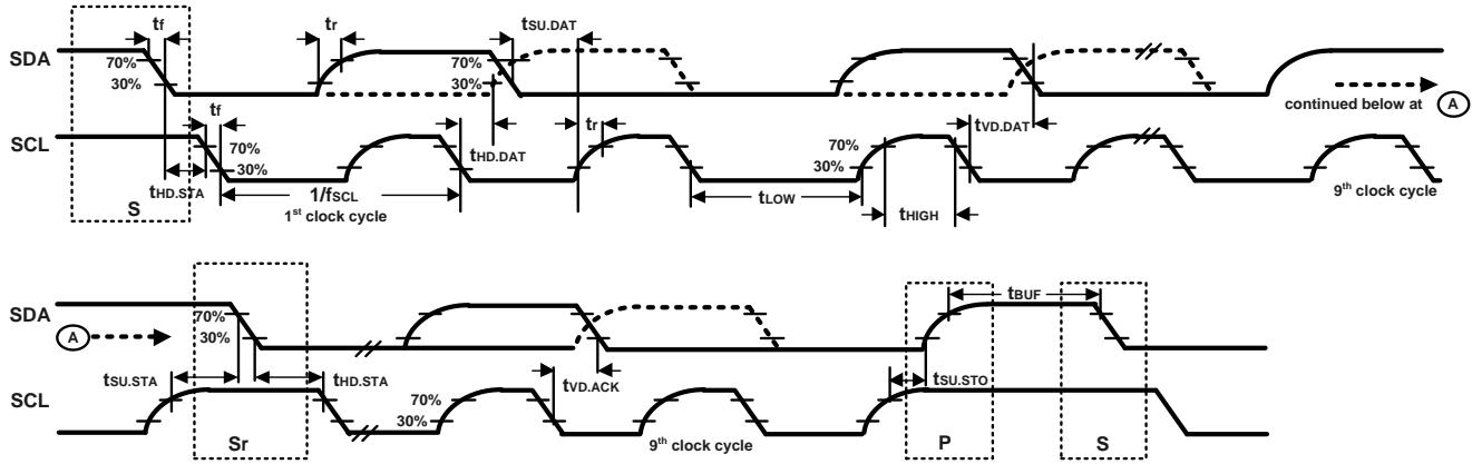
Figure 1. I2C Bus Timing Diagram
3.5 SPI TIMING CHARACTERIZATION – 4-WIRE SPI MODE
Typical Operating Circuit of section 4.2, ${ \mathsf { V D D } } = 1 . 8 { \mathsf { V } } ,$ ${ \mathsf { V D D } } { \mathsf { I O } } = 1 . 8 { \mathsf { V } } ,$ ${ \mathsf { T } } _ { \mathsf { A } } { = } 2 5 ^ { \circ } { \mathsf { C } } ,$ unless otherwise noted.
| PARAMETERS | CONDITIONS | MIN | TYP | MAX | UNITS | NOTES |
| SPI TIMING | ||||||
| $f_{SPC}$ , SCLK Clock Frequency | Default | 24 | MHz | 1 | ||
| $t_{LOW}$ , SCLK Low Period | 17 | ns | 1 | |||
| $t_{HIGH}$ , SCLK High Period | 17 | ns | 1 | |||
| $t_{SU.CS}$ , CS Setup Time | 39 | ns | 1 | |||
| $t_{HD.CS}$ , CS Hold Time | 18 | ns | 1 | |||
| $t_{SU.SDI}$ , SDI Setup Time | 13 | ns | 1 | |||
| $t_{HD.SDI}$ , SDI Hold Time | 8 | ns | 1 | |||
| $t_{VD.SDO}$ , SDO Valid Time | $C_{load}=20 pF$ | 21.5 | ns | 1 | ||
| $t_{HD.SDO}$ , SDO Hold Time | $C_{load}=20 pF$ | 3.5 | ns | 1 | ||
| $t_{DIS.SDO}$ , SDO Output Disable Time | 28 | ns | 1 | |||
| $t_{Fall}$ , SCLK Fall Time | 16 | ns | 2 | |||
| $t_{Rise}$ , SCLK Rise Time | 16 | ns | 2 |
Table 6. 4-Wire SPI Timing Characteristics (24-MHz Operation)
Notes:
Based on characterization of 5 parts over temperature and voltage as mounted on evaluation board or in socket
Based on design and device characterization
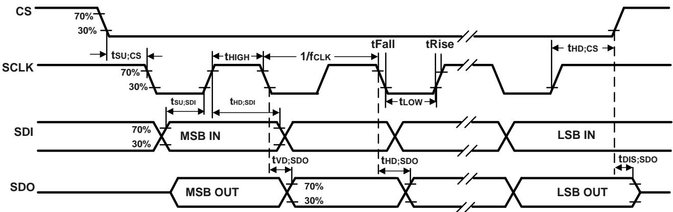
Figure 2. 4-Wire SPI Bus Timing Diagram
3.6 SPI TIMING CHARACTERIZATION – 3-WIRE SPI MODE
Typical Operating Circuit of section 4.2, ${ \mathsf { V D D } } = 1 . 8 { \mathsf { V } } ,$ ${ \mathsf { V D D I O } } = 1 . 8 { \mathsf { V } } ,$ ${ \sf T } _ { \sf A } { = } 2 5 ^ { \circ } { \sf C } ,$ unless otherwise noted.
| PARAMETERS | CONDITIONS | MIN | TYP | MAX | UNITS | NOTES |
| SPI TIMING | ||||||
| $f_{SPC}$ , SCLK Clock Frequency | Default | 24 | MHz | 1 | ||
| $t_{LOW}$ , SCLK Low Period | 17 | ns | 1 | |||
| $t_{HIGH}$ , SCLK High Period | 17 | ns | 1 | |||
| $t_{SU.CS}$ , CS Setup Time | 39 | ns | 1 | |||
| $t_{HD.CS}$ , CS Hold Time | 5 | ns | 1 | |||
| $t_{SU.SDIO}$ , SDIO Input Setup Time | 13 | ns | 1 | |||
| $t_{HD.SDIO}$ , SDIO Input Hold Time | 8 | ns | 1 | |||
| $t_{VD.SDIO}$ , SDIO Output Valid Time | $C_{load}=20 pF$ | 18.5 | ns | 1 | ||
| $t_{HD.SDIO}$ , SDIO Output Hold Time | $C_{load}=20 pF$ | 3.5 | ns | 1 | ||
| $t_{DIS.SDIO}$ , SDIO Output Disable Time | 28 | ns | 1 | |||
| $t_{Fall}$ , SCLK Fall Time | 16 | ns | 2 | |||
| $t_{Rise}$ , SCLK Rise Time | 16 | ns | 2 |
Table 7. 3-Wire SPI Timing Characteristics (24-MHz Operation)
Notes:
- Based on characterization of 5 parts over temperature and voltage as mounted on evaluation board or in sockets
- Based on design and device characterization
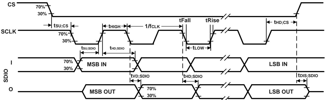
Figure 3. 3-Wire SPI Bus Timing Diagram
3.7 RTC (CLKIN) TIMING CHARACTERIZATION
Typical Operating Circuit of section 4.2, VDD = 1.8 V, ${ \mathsf { V D D I O } } = 1 . 8 { \mathsf { V } } ,$ ${ \mathsf { T } } _ { \mathsf { A } } { = } 2 5 ^ { \circ } { \mathsf { C } } ,$ unless otherwise noted.
| PARAMETERS | CONDITIONS | MIN | TYP | MAX | UNITS | NOTES |
| RTC (CLKIN) TIMING | ||||||
| $F_{\text{RTC}}$ , RTC Clock Frequency | Default | 31 | 32 | 50 | kHz | |
| $t_{\text{HIGHRTC}}$ , RTC Clock High Period | 1 | μs | ||||
| $t_{\text{RiseRTC}}$ , RTC Clock Rise Time | 5 | 500 | ns | |||
| $t_{\text{FallRTC}}$ , RTC Clock Fall Time | 5 | 500 | ns |
Table 8. RTC Timing Characteristics

Figure 4. RTC Timing Diagram
3.8 ABSOLUTE MAXIMUM RATINGS
Stress above those listed as “Absolute Maximum Ratings” may cause permanent damage to the device. These are stress ratings only and functional operation of the device at these conditions is not implied. Exposure to the absolute maximum ratings conditions for extended periods may affect device reliability.
| Parameter | Rating |
| Supply Voltage, VDD | -0.5 V to +4 V |
| Supply Voltage, VDDIO | -0.5 V to +4 V |
| Input Voltage Level (FSYNC, SCL, SDA) | -0.5 V to VDDIO + 0.5 V |
| Acceleration (Any Axis, unpowered) | 20,000g for 0.2 ms |
| Operating Temperature Range | -40°C to +85°C |
| Storage Temperature Range | -40°C to +125°C |
| Electrostatic Discharge (ESD) Protection | 2 kV (HBM);500 V (CDM) |
| Latch-up | JEDEC Class II (2),125°C±100 mA |
Table 9. Absolute Maximum Ratings
4 APPLICATIONS INFORMATION
4.1 PIN OUT DIAGRAM AND SIGNAL DESCRIPTION
| Pin Number | Pin Name | Pin Description |
| 1 | AP_SDO / AP_ADO | AP_SDO: AP SPI serial data output (4-wire mode);AP_ADO: AP $I3C^{SM}$ / $I^{2}C$ slave address LSB |
| 2 | RESV | No Connect or Connect to GND |
| 3 | RESV | No Connect or Connect to GND |
| 4 | INT1 / INT | INT1: Interrupt 1 (Note: INT1 can be push-pull or open drain)INT: All interrupts mapped to pin 4 |
| 5 | VDDIO | IO power supply voltage |
| 6 | GND | Power supply ground |
| 7 | RESV | Connect to GND |
| 8 | VDD | Power supply voltage |
| 9 | INT2 / FSYNC / CLKIN | INT2: Interrupt 2 (Note: INT2 can be push-pull or open drain)FSYNC: Frame sync input; Connect to GND if FSYNC not usedCLKIN: External clock input |
| 10 | RESV | No Connect or Connect to GND |
| 11 | RESV | No Connect or Connect to GND |
| 12 | AP_CS | AP SPI Chip select (AP SPI interface); Connect to VDDIO if using AP $I3C^{SM}$ / $I^{2}C$ interface |
| 13 | AP_SCL / AP_SCLK | AP_SCL: AP $I3C^{SM}$ / $I^{2}C$ serial clock; AP_SCLK: AP SPI serial clock |
| 14 | AP_SDA / AP_SDIO /AP_SDI | AP_SDA: AP $I3C^{SM}$ / $I^{2}C$ serial data; AP_SDIO: AP SPI serial data I/O (3-wire mode); AP_SDI: AP SPI serial data input (4-wire mode) |
Table 10. Signal Descriptions
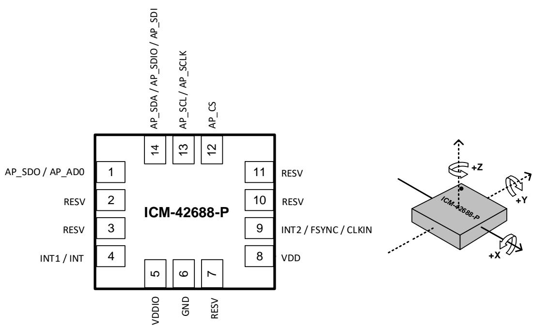
Figure 5. Pin Out Diagram for ICM-42688-P 2.5x3.0x0.91 mm LGA
4.2 TYPICAL OPERATING CIRCUIT

Figure 6. ICM-42688-P Application Schematic (I3CSM / I2C Interface to Host)
Note: I2C lines are open drain and pull-up resistors (e.g. 10 kΩ) are required.

Figure 7. ICM-42688-P Application Schematic (SPI Interface to Host)
4.3 BILL OF MATERIALS FOR EXTERNAL COMPONENTS
| Component | Label | Specification | Quantity |
| VDD Bypass Capacitors | C1 | X7R, 0.1μF ±10% | 1 |
| C2 | X7R, 2.2μF ±10% | 1 | |
| VDDIO Bypass Capacitor | C3 | X7R, 10nF ±10% | 1 |
Table 11. Bill of Materials
4.4 SYSTEM BLOCK DIAGRAM

Figure 8. ICM-42688-P System Block Diagram
Note: The above block diagram is an example. Please refer to the pin-out (section 4.1) for other configuration options.
4.5 OVERVIEW
The ICM-42688-P is comprised of the following key blocks and functions:
• Three-axis MEMS rate gyroscope sensor with 16-bit ADCs and signal conditioning
o 20-bits data format support in FIFO for high-data resolution (see section 6 for details)
• Three-axis MEMS accelerometer sensor with 16-bit ADCs and signal conditioning
o 20-bits data format support in FIFO for high-data resolution (see section 6 for details)
${ \mathsf { I } } { \mathsf { 3 C } } ^ { \mathsf { S M } } ,$ I2C and SPI serial communications interfaces
• Self-Test
• Clocking
• Sensor Data Registers
FIFO
• Interrupts
● Digital-Output Temperature Sensor
• Bias and LDOs
• Charge Pump
• Standard Power Modes
4.6 THREE-AXIS MEMS GYROSCOPE WITH 16-BIT ADCS AND SIGNAL CONDITIONING
The ICM-42688-P includes a vibratory MEMS rate gyroscope, which detects rotation about the X-, Y-, and Z- Axes. When the gyroscope is rotated about any of the sense axes, the Coriolis Effect causes a vibration that is detected by a capacitive pickoff. The resulting signal is amplified, demodulated, and filtered to produce a voltage that is proportional to the angular rate. This voltage is digitized using on-chip Analog-to-Digital Converters (ADCs) to sample each axis. The full-scale range of the gyro sensors may be digitally programmed to ±15.625, ±31.25, ±62.5, ±125, ±250, ±500, ±1000, and ±2000 degrees per second (dps).
4.7 THREE-AXIS MEMS ACCELEROMETER WITH 16-BIT ADCS AND SIGNAL CONDITIONING
The ICM-42688-P includes a 3-Axis MEMS accelerometer. Acceleration along a particular axis induces displacement of a proof mass in the MEMS structure, and capacitive sensors detect the displacement. The ICM-42688-P architecture reduces the accelerometers susceptibility to fabrication variations as well as to thermal drift. When the device is placed on a flat surface, it will measure 0g on the X- and Y-axes and +1g on the Z-axis. The accelerometers’ scale factor is calibrated at the factory and is nominally independent of supply voltage. The full-scale range of the digital output can be adjusted to ±2g, ±4g, ±8g and ±16g.
4.8 I3CSM, I2C AND SPI HOST INTERFACE
The ICM-42688-P communicates to the application processor using an ${ \mathsf { I } } 3 { \mathsf { C } } ^ { \mathsf { S M } } ,$ , I2C, or SPI serial interface. The ICM-42688-P always acts as a slave when communicating to the application processor.
4.9 SELF-TEST
Self-test allows for the testing of the mechanical and electrical portions of the sensors. The self-test for each measurement axis can be activated by means of the gyroscope and accelerometer self-test registers.
When the self-test is activated, the electronics cause the sensors to be actuated and produce an output signal. The output signal is used to observe the self-test response.
The self-test response is defined as follows:
Self-test response = Sensor output with self-test enabled – Sensor output with self-test disabled
When the value of the self-test response is within the specified min/max limits of the product specification, the part has passed selftest. When the self-test response exceeds the min/max values, the part is deemed to have failed self-test.
4.10 CLOCKING
The ICM-42688-P has a flexible clocking scheme, allowing external or internal clock sources to be used for the internal synchronous circuitry. This synchronous circuitry includes the signal conditioning and ADCs, and various control circuits and registers.
The CLKIN pin on ICM-42688-P provides the ability to input an external clock. A highly accurate external clock may be used rather than the internal clocks sources, if greater clock accuracy is desired. External clock input supports highly accurate clock input from 31kHz to 50kHz, resulting in improvement of the following:
a) ODR uncertainty due to process, temperature, operating mode (PLL vs. RCOSC), and design limitations. This uncertainty can be as high as ±8% in RCOSC mode and ±1% in PLL mode. The CLKIN, assuming a 50ppm or better 32.768kHz source, wil improve the ODR accuracy from ±80,000ppm to ±50ppm in RCOSC mode, or from ±10,000ppm to ±50ppm in PLL mode.
b) System level sensitivity error. Any clock uncertainty directly impacts gyroscope sensitivity at the system level. Sophisticated systems can estimate ODR inaccuracy to some extent, but not to the extent improved by using CLKIN.
c) System-level clock/sensor synchronization. When using CLKIN, the accelerometer and gyroscope are on the same clock as the host. There is no need to continually re-synchronize the sensor data as the sensor sample points and period are known to be in exact alignment with the common system clock.
d) CLKIN helps EIS (Electronic Image Stabilization) performance by providing:
o Very accurate gyroscope sample points for use during integration to find true angular displacement.
o Automatic time alignment between the motion sensor and the host and potentially the camera system.
e) Other applications that benefit from CLKIN include navigation, gaming, robotics.
Allowable internal sources for generating the internal clock are:
a) An internal relaxation oscillator
b) Auto-select between internal relaxation oscillator and gyroscope MEMS oscillator to use the best available source
For internal sources, the only setting supporting specified performance in all modes is option b). It is recommended that option b) be used when using internal clock source.
4.11 SENSOR DATA REGISTERS
The sensor data registers contain the latest gyroscope, accelerometer, and temperature measurement data. They are read-only registers, and are accessed via the serial interface. Data from these registers may be read anytime.
4.12 INTERRUPTS
Interrupt functionality is configured via the Interrupt Configuration register. Items that are configurable include the interrupt pins configuration, the interrupt latching and clearing method, and triggers for the interrupt. Items that can trigger an interrupt are (1) Clock generator locked to new reference oscillator (used when switching clock sources); (2) new data is available to be read (from the FIFO and Data registers); (3) accelerometer event interrupts; (4) FIFO watermark; (5) FIFO overflow. The interrupt status can be read from the Interrupt Status register.
4.13 DIGITAL-OUTPUT TEMPERATURE SENSOR
An on-chip temperature sensor and ADC are used to measure the ICM-42688-P die temperature. The readings from the ADC can be read from the FIFO or the Sensor Data registers.
Temperature sensor register data TEMP_DATA is updated with new data at max(Accelerometer ODR, Gyroscope ODR).
Temperature data value from the sensor data registers can be converted to degrees centigrade by using the following formula:
Temperature in Degrees Centigrade = (TEMP_DATA / 132.48) + 25
Temperature data stored in FIFO is an 8-bit quantity, FIFO_TEMP_DATA. It can be converted to degrees centigrade by using the following formula:
Temperature in Degrees Centigrade = (FIFO_TEMP_DATA / 2.07) + 25
4.14 BIAS AND LDOS
The bias and LDO section generates the internal supply and the reference voltages and currents required by the ICM-42688-P.
4.15 CHARGE PUMP
An on-chip charge pump generates the high voltage required for the MEMS oscillator.
4.16 STANDARD POWER MODES
The following table lists the user-accessible power modes for ICM-42688-P.
| Mode | Name | Gyro | Accel |
| 1 | Sleep Mode | Off | Off |
| 2 | Standby Mode | Drive On | Off |
| 3 | Accelerometer Low-Power Mode | Off | Duty-Cycled |
| 4 | Accelerometer Low-Noise Mode | Off | On |
| 5 | Gyroscope Low-Noise Mode | On | Off |
| 6 | 6-Axis Low-Noise Mode | On | On |
Table 12. Standard Power Modes for ICM-42688-P
5 SIGNAL PATH
The following figure shows a block diagram of the signal path for ICM-42688-P.

Figure 9. ICM-42688-P Signal Path
The signal path starts with ADCs for the gyroscope and accelerometer. Other components of the signal path are described below in further detail.
5.1 SUMMARY OF PARAMETERS USED TO CONFIGURE THE SIGNAL PATH
The following table shows the parameters that can control the signal path.
| Parameter Name | Description |
| GYRO_AAF_DIS | Disables the Gyroscope Anti Alias Filter (AAF) |
| GYRO_AAF_DELT | Three parameters required to program the gyroscope AAF. This is a $2^{nd}$ order filter with programmable low pass filter. This is a user programmable filter which can be used to select the desired BW. This filter allows trading off RMS noise vs. latency for a given ODR. |
| GYRO_AAF_DELTSQR | |
| GYRO_AAF_BITSHIFT | |
| ACCEL_AAF_DIS | Disables the Accelerometer Anti Alias Filter |
| ACCEL_AAF_DEL | Three parameters required to program the accelerometer AAF. This is a $2^{nd}$ order filter with programmable low pass filter. This is a user programmable filter which can be used to select the desired BW. This filter allows trading off RMS noise vs. latency for a given ODR. |
| ACCEL_AAF_DELTSQR | |
| ACCEL_AAF_BITSHIFT | |
| GYRO_NF_DIS | Disables the gyro Notch Filter |
| GYRO_X/Y/Z_NF_COSWZ | Factory trimmed parameters, designed to position a Notch at or near the sense peak frequency of Gyro. This allows the user to suppress only sense peak contribution to noise, while still maintaining a low latency high BW/ODR interface from the Sensor. This filter is available only in Gyro, and the parameters for X, Y, and Z are chosen independently. |
| GYRO_X/Y/Z_NF_COSWZ_SEL | |
| GYRO_X/Y/Z_NF_COSWZ_SEL | |
| GYRO_NF_BW_SEL | Factory trimmed parameter to cancel noise created by sense peak from Gyro. This parameter is common to all three axes |
5.2 NOTCH FILTER
The Notch Filter is supported only for the gyroscope signal path. The following steps can be used to program the notch filter. Note that the notch filter is specific to each axis in the gyroscope, so the X, Y and Z axis can be programmed independently.
Frequency of Notch Filter (each axis)
To operate the Notch filter, two parameters NF_COSWZ, and NF_COSWZ_SEL must be programmed for each gyroscope axis.
Parameters NF_COSWZ are defined for each axis of the gyroscope as GYRO_X_NF_COSWZ (register bank 1, register 0x0Fh & registe 0x12h), GYRO_Y_NF_COSWZ (register bank 1, register 0x10h & register 0x12h), GYRO_Z_NF_COSWZ (register bank 1, register 0x11h & register 0x12h). Note that the parameters have 9-bit values across two different registers.
Parameters NF_COSWZ_SEL are defined for each axis of the gyroscope as GYRO_X_NF_COSWZ_SEL (register bank 1, register 0x12h, bit 3), GYRO_Y_NF_COSWZ_SEL (register bank 1, register 0x12h, bit 4), GYRO_Z_NF_COSWZ_SEL (register bank 1, register 0x12h, bit 5).
Each value must be calculated using the steps described below, and programmed into the corresponding register locations mentioned above.
fdesired is the desired frequency of the Notch Filter in kHz. The lower bound for fdesired is 1kHz, and the upper bound is 3kHz. Operating the notch filter outside this range is not supported.
Step1: Fdrv = 19.2MHz/(CLKDIV*10); See Bank 3 register 0x2A for CLKDIV
Step2: COSWZ = cos(2*pi*fdesired/Fdrv)
Step3:
If abs(COSWZ)≤0.875
    NF_COSWZ = round[COSWZ*256]
    NF_COSWZ_SEL = 0
else
    NF_COSWZ_SEL = 1
    if COSWZ > 0.875
    NF_COSWZ = round [8*(1-COSWZ)*256]
    else if COSWZ < -0.875
    NF_COSWZ = round [-8*(1+COSWZ)*256]
    end
End
Bandwidth of Notch Filter (common to all axes)
The notch filter allows the user to control the width of the notch from eight possible values using a 3-bit parameter GYRO_NF_BW_SEL in register bank 1, register 0x13h, bits 6:4. This parameter is common to all three axes.
| GYRO_NF_BW_SEL | Notch Filter Bandwidth (Hz) |
| 0 | 1449 |
| 1 | 680 |
| 2 | 329 |
| 3 | 162 |
| 4 | 80 |
| 5 | 40 |
| 6 | 20 |
| 7 | 10 |
The notch filter can be selected or bypassed by using the parameter GYRO_NF_DIS in register bank 1, register 0x0Bh, bit 0 as shown below.
| GYRO_NF_DIS | Function |
| 0 | Enable notch filter |
| 1 | Disable notch filter |
5.3 ANTI-ALIAS FILTER
Anti-alias filters for gyroscope and accelerometer can be independently programmed to have bandwidths ranging from 42 Hz to 3979 Hz. To program the anti-alias filter for a required bandwidth, use the table below to map the bandwidth to register values as shown:
a. Register bank 2, register 0x03h, bits 6:1, ACCEL_AAF_DELT: Code from 1 to 63 that allows programming the bandwidth for accelerometer anti-alias filter
b. Register bank 2, register 0x04h, bits 7:0 and Bank 2, register 0x05h, bits 3:0, ACCEL_AAF_DELTSQR: Square of the delt value for accelerometer
c. Register bank 2, register 0x05h, bits 7:4, ACCEL_AAF_BITSHIFT: Bitshift value for accelerometer used in hardware implementation
d. Register bank 1, register 0x0Ch, bits 5:0, GYRO_AAF_DELT: Code from 1 to 63 that allows programming the bandwidth for gyroscope anti-alias filter
e. Register bank 1, register 0x0Dh, bits 7:0 and Bank 1, register 0x0Eh, bits 3:0, GYRO_AAF_DELTSQR: Square of the delt value for gyroscope
f. Register bank 1, register 0x0Eh, bits 7:4, GYRO_AAF_BITSHIFT: Bitshift value for gyroscope used in hardware implementation
| 3dB Bandwidth (Hz) | ACCEL_AAF_DELT; GYRO_AAF_DELT | ACCEL_AAF_DELTSQR; GYRO_AAF_DELTSQR | ACCEL_AAF_BITSHIFT; GYRO_AAF_BITSHIFT |
| 42 | 1 | 1 | 15 |
| 84 | 2 | 4 | 13 |
| 126 | 3 | 9 | 12 |
| 170 | 4 | 16 | 11 |
| 213 | 5 | 25 | 10 |
| 258 | 6 | 36 | 10 |
| 303 | 7 | 49 | 9 |
| 348 | 8 | 64 | 9 |
| 394 | 9 | 81 | 9 |
| 441 | 10 | 100 | 8 |
| 488 | 11 | 122 | 8 |
| 536 | 12 | 144 | 8 |
| 585 | 13 | 170 | 8 |
| 634 | 14 | 196 | 7 |
| 684 | 15 | 224 | 7 |
| 734 | 16 | 256 | 7 |
| 785 | 17 | 288 | 7 |
| 837 | 18 | 324 | 7 |
| 890 | 19 | 360 | 6 |
| 943 | 20 | 400 | 6 |
| 997 | 21 | 440 | 6 |
| 1051 | 22 | 488 | 6 |
| 1107 | 23 | 528 | 6 |
| 1163 | 24 | 576 | 6 |
| 1220 | 25 | 624 | 6 |
| 1277 | 26 | 680 | 6 |
| 1336 | 27 | 736 | 5 |
| 1395 | 28 | 784 | 5 |
| 1454 | 29 | 848 | 5 |
| 1515 | 30 | 896 | 5 |
| 1577 | 31 | 960 | 5 |
| 1639 | 32 | 1024 | 5 |
| 1702 | 33 | 1088 | 5 |
| 1766 | 34 | 1152 | 5 |
| 1830 | 35 | 1232 | 5 |
| 1896 | 36 | 1296 | 5 |
| 1962 | 37 | 1376 | 4 |
| 2029 | 38 | 1440 | 4 |
| 2097 | 39 | 1536 | 4 |
| 2166 | 40 | 1600 | 4 |
| 2235 | 41 | 1696 | 4 |
| 2306 | 42 | 1760 | 4 |
| 2377 | 43 | 1856 | 4 |
| 2449 | 44 | 1952 | 4 |
| 2522 | 45 | 2016 | 4 |
| 2596 | 46 | 2112 | 4 |
| 2671 | 47 | 2208 | 4 |
| 2746 | 48 | 2304 | 4 |
| 2823 | 49 | 2400 | 4 |
| 2900 | 50 | 2496 | 4 |
| 2978 | 51 | 2592 | 4 |
| 3057 | 52 | 2720 | 4 |
| 3137 | 53 | 2816 | 3 |
| 3217 | 54 | 2944 | 3 |
| 3299 | 55 | 3008 | 3 |
| 3381 | 56 | 3136 | 3 |
| 3464 | 57 | 3264 | 3 |
| 3548 | 58 | 3392 | 3 |
| 3633 | 59 | 3456 | 3 |
| 3718 | 60 | 3584 | 3 |
| 3805 | 61 | 3712 | 3 |
| 3892 | 62 | 3840 | 3 |
| 3979 | 63 | 3968 | 3 |
The anti-alias filter can be selected or bypassed for the gyroscope by using the parameter GYRO_AAF_DIS in register bank 1, register 0x0Bh, bit 1 as shown below.
| GYRO_AAF_DIS | Function |
| 0 | Enable gyroscope anti-aliasing filter |
| 1 | Disable gyroscope anti-aliasing filter |
The anti-alias filter can be selected or bypassed for the accelerometer by using the parameter ACCEL_AAF_DIS in register bank 2, register 0x03h, bit 0 as shown below.
| ACCEL_AAF_DIS | Function |
| 0 | Enable accelerometer anti-aliasing filter |
| 1 | Disable accelerometer anti-aliasing filter |
5.4 USER PROGRAMMABLE OFFSET
Gyroscope and accelerometer offsets can be programmed by the user by using registers OFFSET_USER0, through OFFSET_USER8, in bank 0, registers 0x77h through 0x7Fh (bank 4) as shown below.
| Register Address | Register Name | Bits | Function |
| 0x77h | OFFSET_USER0 | 7:0 | Lower bits of X-gyro offset programmed by user.Max value is ±64 dps, resolution is 1/32 dps. |
| 0x78h | OFFSET_USER1 | 3:0 | Upper bits of X-gyro offset programmed by user.Max value is ±64 dps, resolution is 1/32 dps. |
| 7:4 | Upper bits of Y-gyro offset programmed by user.Max value is ±64 dps, resolution is 1/32 dps. | ||
| 0x79h | OFFSET_USER2 | 7:0 | Lower bits of Y-gyro offset programmed by user.Max value is ±64 dps, resolution is 1/32 dps. |
| 0x7Ah | OFFSET_USER3 | 7:0 | Lower bits of Z-gyro offset programmed by user.Max value is ±64 dps, resolution is 1/32 dps. |
| 0x7Bh | OFFSET_USER4 | 3:0 | Upper bits of Z-gyro offset programmed by user.Max value is ±64 dps, resolution is 1/32 dps. |
| 7:4 | Upper bits of X-accel offset programmed by user.Max value is ±1 g, resolution is 0.5 g. | ||
| 0x7Ch | OFFSET_USER5 | 7:0 | Lower bits of X-accel offset programmed by user.Max value is ±1 g, resolution is 0.5 g. |
| 0x7Dh | OFFSET_USER6 | 7:0 | Lower bits of Y-accel offset programmed by user.Max value is ±1 g, resolution is 0.5 g. |
| 0x7Eh | OFFSET_USER7 | 3:0 | Upper bits of Y-accel offset programmed by user.Max value is ±1 g, resolution is 0.5 g. |
| 7:4 | Upper bits of Z-accel offset programmed by user.Max value is ±1 g, resolution is 0.5 g. | ||
| 0x7Fh | OFFSET_USER8 | 7:0 | Lower bits of Z-accel offset programmed by user.Max value is ±1 g, resolution is 0.5 g. |
5.5 UI FILTER BLOCK
The UI filter block can be programmed to select filter order and bandwidth independently for gyroscope and accelerometer.
Gyroscope filter order can be selected by programming the parameter GYRO_UI_FILT_ORD in register bank 0, register 0x51h, bits 3:2, as shown below.
| GYRO_UI_FILT_ORD | Filter Order |
| 00 | $1^{st}$ order |
| 01 | $2^{nd}$ order |
| 10 | $3^{rd}$ order |
| 11 | Reserved |
Accelerometer filter order can be selected by programming the parameter ACCEL_UI_FILT_ORD in register bank 0, register 0x53h, bits 4:3, as shown below.
| ACCEL_UI_FILT_ORD | Filter Order |
| 00 | $1^{st}$ order |
| 01 | $2^{nd}$ order |
| 10 | $3^{rd}$ order |
| 11 | Reserved |
Gyroscope and accelerometer filter 3dB bandwidth can be selected by programming the parameter GYRO_UI_FILT_BW in register bank 0, register 0x52h, bits 3:0, and the parameter ACCEL_UI_FILT_BW in register bank 0, register 0x52h, bits 7:4, as shown below. The values shown in bold correspond to low noise and the values shown in italics correspond to low latency. User can select the appropriate setting based on the application requirements for power and latency. Corresponding Noise Bandwidth (NBW) and Group Delay values are also shown.
1st Order Filter 3dB Bandwidth, Noise Bandwidth (NBW), Group Delay
| 3dB Bandwidth (Hz) for GYRO/ACCEL_UI_FILT_ORD=0 (1st order filter) | |||||||||||
| GYRO/ACCEL_UI_FILT_BW | |||||||||||
| GYRO/ACCEL_ODR | ODR(Hz) | 0 | 1 | 2 | 3 | 4 | 5 | 6 | 7 | 14 | 15 |
| 1 | 32000 | 8400.0 | |||||||||
| 2 | 16000 | 4194.1 | |||||||||
| 3 | 8000 | 2096.3 | |||||||||
| 4 | 4000 | 1048.1 | |||||||||
| 5 | 2000 | 524.0 | |||||||||
| 6 | 1000 | 498.3 | 227.2 | 188.9 | 111.0 | 92.4 | 59.6 | 48.8 | 23.9 | 262.0 | 2096.3 |
| 15 | 500 | 249.1 | 113.6 | 94.4 | 55.5 | 46.2 | 29.8 | 24.4 | 11.9 | 131.0 | 1048.1 |
| 7 | 200 | 99.6 | 90.9 | 75.5 | 44.4 | 37.0 | 23.8 | 19.5 | 9.6 | 104.8 | 419.2 |
| 8 | 100 | 49.8 | 90.9 | 75.5 | 44.4 | 37.0 | 23.8 | 19.5 | 9.6 | 104.8 | 209.6 |
| 9 | 50 | 24.9 | 90.9 | 75.5 | 44.4 | 37.0 | 23.8 | 19.5 | 9.6 | 104.8 | 104.8 |
| 10 | 25 | 12.5 | 90.9 | 75.5 | 44.4 | 37.0 | 23.8 | 19.5 | 9.6 | 104.8 | 52.4 |
| 11 | 12.5 | 12.5 | 90.9 | 75.5 | 44.4 | 37.0 | 23.8 | 19.5 | 9.6 | 104.8 | 52.4 |
| NBW Bandwidth (Hz) for GYRO/ACCEL_UI_FILT_ORD=0 (1st order filter) | |||||||||||
| GYRO/ACCEL_UI_FILT_BW | |||||||||||
| GYRO/ACCEL_ODR | ODR(Hz) | 0 | 1 | 2 | 3 | 4 | 5 | 6 | 7 | 14 | 15 |
| 1 | 32000 | 8831.7 | |||||||||
| 2 | 16000 | 4410.6 | |||||||||
| 3 | 8000 | 2204.6 | |||||||||
| 4 | 4000 | 1102.2 | |||||||||
| 5 | 2000 | 551.1 | |||||||||
| 6 | 1000 | 551.1 | 230.8 | 196.3 | 126.5 | 108.9 | 75.8 | 64.1 | 34.1 | 275.6 | 2204.6 |
| 15 | 500 | 280.5 | 115.4 | 98.2 | 63.3 | 54.5 | 37.9 | 32.1 | 17.1 | 137.8 | 1102.2 |
| 7 | 200 | 112.2 | 92.4 | 78.5 | 50.6 | 43.6 | 30.3 | 25.7 | 13.7 | 110.3 | 440.9 |
| 8 | 100 | 56.1 | 92.4 | 78.5 | 50.6 | 43.6 | 30.3 | 25.7 | 13.7 | 110.3 | 220.5 |
| 9 | 50 | 28.1 | 92.4 | 78.5 | 50.6 | 43.6 | 30.3 | 25.7 | 13.7 | 110.3 | 110.3 |
| 10 | 25 | 14.1 | 92.4 | 78.5 | 50.6 | 43.6 | 30.3 | 25.7 | 13.7 | 110.3 | 55.2 |
| 11 | 12.5 | 14.1 | 92.4 | 78.5 | 50.6 | 43.6 | 30.3 | 25.7 | 13.7 | 110.3 | 55.2 |
| Group Delay @DC (ms) for GYRO/ACCEL_UI_FILT_ORD=0 (1st order filter) | |||||||||||
| GYRO/ACCEL_UI_FILT_BW | |||||||||||
| GYRO/ACCEL_ODR | ODR(Hz) | 0 | 1 | 2 | 3 | 4 | 5 | 6 | 7 | 14 | 15 |
| 1 | 32000 | 0.1 | |||||||||
| 2 | 16000 | 0.1 | |||||||||
| 3 | 8000 | 0.2 | |||||||||
| 4 | 4000 | 0.4 | |||||||||
| 5 | 2000 | 0.8 | |||||||||
| 6 | 1000 | 0.6 | 1.8 | 2.0 | 2.8 | 3.1 | 4.1 | 4.7 | 8.1 | 1.5 | 0.2 |
| 15 | 500 | 1.1 | 3.6 | 4.0 | 5.5 | 6.1 | 8.1 | 9.3 | 16.2 | 3.0 | 0.4 |
| 7 | 200 | 2.7 | 4.4 | 5.0 | 6.8 | 7.6 | 10.2 | 11.7 | 20.3 | 3.8 | 1.0 |
| 8 | 100 | 5.3 | 4.4 | 5.0 | 6.8 | 7.6 | 10.2 | 11.7 | 20.3 | 3.8 | 1.9 |
| 9 | 50 | 10.5 | 4.4 | 5.0 | 6.8 | 7.6 | 10.2 | 11.7 | 20.3 | 3.8 | 3.8 |
| 10 | 25 | 21.0 | 4.4 | 5.0 | 6.8 | 7.6 | 10.2 | 11.7 | 20.3 | 3.8 | 7.5 |
| 11 | 12.5 | 21.0 | 4.4 | 5.0 | 6.8 | 7.6 | 10.2 | 11.7 | 20.3 | 3.8 | 7.5 |
2nd Order Filter 3dB Bandwidth, Noise Bandwidth (NBW), Group Delay
| 3dB Bandwidth (Hz) for GYRO/ACCEL_UI_FILT_ORD=1 (2nd order filter) | |||||||||||
| GYRO/ACCEL_UI_FILT_BW | |||||||||||
| GYRO/ACCEL_ODR | ODR(Hz) | 0 | 1 | 2 | 3 | 4 | 5 | 6 | 7 | 14 | 15 |
| 1 | 32000 | 8400.0 | |||||||||
| 2 | 16000 | 4194.1 | |||||||||
| 3 | 8000 | 2096.3 | |||||||||
| 4 | 4000 | 1048.1 | |||||||||
| 5 | 2000 | 524.0 | |||||||||
| 6 | 1000 | 493.3 | 230.7 | 191.6 | 117.5 | 97.1 | 59.6 | 48.0 | 21.3 | 262.0 | 2096.3 |
| 15 | 500 | 246.7 | 115.3 | 95.8 | 58.8 | 48.5 | 29.8 | 24.0 | 10.6 | 131.0 | 1048.1 |
| 7 | 200 | 98.7 | 92.3 | 76.6 | 47.0 | 38.8 | 23.8 | 19.2 | 8.5 | 104.8 | 419.2 |
| 8 | 100 | 49.3 | 92.3 | 76.6 | 47.0 | 38.8 | 23.8 | 19.2 | 8.5 | 104.8 | 209.6 |
| 9 | 50 | 24.7 | 92.3 | 76.6 | 47.0 | 38.8 | 23.8 | 19.2 | 8.5 | 104.8 | 104.8 |
| 10 | 25 | 12.3 | 92.3 | 76.6 | 47.0 | 38.8 | 23.8 | 19.2 | 8.5 | 104.8 | 52.4 |
| 11 | 12.5 | 12.3 | 92.3 | 76.6 | 47.0 | 38.8 | 23.8 | 19.2 | 8.5 | 104.8 | 52.4 |
| NBW Bandwidth (Hz) for GYRO/ACCEL_UI_FILT_ORD=1 (2nd order filter) | |||||||||||
| GYRO/ACCEL_UI_FILT_BW | |||||||||||
| GYRO/ACCEL_ODR | ODR(Hz) | 0 | 1 | 2 | 3 | 4 | 5 | 6 | 7 | 14 | 15 |
| 1 | 32000 | 8831.7 | |||||||||
| 2 | 16000 | 4410.6 | |||||||||
| 3 | 8000 | 2204.6 | |||||||||
| 4 | 4000 | 1102.2 | |||||||||
| 5 | 2000 | 551.1 | |||||||||
| 6 | 1000 | 551.1 | 223.7 | 189.9 | 122.7 | 102.8 | 64.7 | 52.5 | 23.7 | 275.6 | 2204.6 |
| 15 | 500 | 259.6 | 111.9 | 95.0 | 61.4 | 51.4 | 32.4 | 26.3 | 11.9 | 137.8 | 1102.2 |
| 7 | 200 | 103.9 | 89.5 | 76.0 | 49.1 | 41.2 | 25.9 | 21.0 | 9.5 | 110.3 | 440.9 |
| 8 | 100 | 52.0 | 89.5 | 76.0 | 49.1 | 41.2 | 25.9 | 21.0 | 9.5 | 110.3 | 220.5 |
| 9 | 50 | 26.0 | 89.5 | 76.0 | 49.1 | 41.2 | 25.9 | 21.0 | 9.5 | 110.3 | 110.3 |
| 10 | 25 | 13.0 | 89.5 | 76.0 | 49.1 | 41.2 | 25.9 | 21.0 | 9.5 | 110.3 | 55.2 |
| 11 | 12.5 | 13.0 | 89.5 | 76.0 | 49.1 | 41.2 | 25.9 | 21.0 | 9.5 | 110.3 | 55.2 |
| Group Delay @DC (ms) for GYRO/ACCEL_UI_FILT_ORD=1 (2nd order filter) | |||||||||||
| GYRO/ACCEL_UI_FILT_BW | |||||||||||
| GYRO/ACCEL_ODR | ODR(Hz) | 0 | 1 | 2 | 3 | 4 | 5 | 6 | 7 | 14 | 15 |
| 1 | 32000 | 0.1 | |||||||||
| 2 | 16000 | 0.1 | |||||||||
| 3 | 8000 | 0.2 | |||||||||
| 4 | 4000 | 0.4 | |||||||||
| 5 | 2000 | 0.8 | |||||||||
| 6 | 1000 | 0.7 | 2.1 | 2.4 | 3.2 | 3.7 | 5.2 | 6.1 | 12.0 | 1.5 | 0.2 |
| 15 | 500 | 1.3 | 4.1 | 4.7 | 6.4 | 7.3 | 10.4 | 12.2 | 24.0 | 3.0 | 0.4 |
| 7 | 200 | 3.3 | 5.1 | 5.8 | 8.0 | 9.1 | 12.9 | 15.3 | 30.0 | 3.8 | 1.0 |
| 8 | 100 | 6.5 | 5.1 | 5.8 | 8.0 | 9.1 | 12.9 | 15.3 | 30.0 | 3.8 | 1.9 |
| 9 | 50 | 12.9 | 5.1 | 5.8 | 8.0 | 9.1 | 12.9 | 15.3 | 30.0 | 3.8 | 3.8 |
| 10 | 25 | 25.7 | 5.1 | 5.8 | 8.0 | 9.1 | 12.9 | 15.3 | 30.0 | 3.8 | 7.5 |
| 11 | 12.5 | 25.7 | 5.1 | 5.8 | 8.0 | 9.1 | 12.9 | 15.3 | 30.0 | 3.8 | 7.5 |
3rd Order Filter 3dB Bandwidth, Noise Bandwidth (NBW), Group Delay
| 3dB Bandwidth (Hz) for GYRO/ACCEL_UI_FILT_ORD=2 (3rd order filter) | |||||||||||
| GYRO/ACCEL_UI_FILT_BW | |||||||||||
| GYRO/ACCEL_ODR | ODR(Hz) | 0 | 1 | 2 | 3 | 4 | 5 | 6 | 7 | 14 | 15 |
| 1 | 32000 | 8400.0 | |||||||||
| 2 | 16000 | 4194.1 | |||||||||
| 3 | 8000 | 2096.3 | |||||||||
| 4 | 4000 | 1048.1 | |||||||||
| 5 | 2000 | 524.0 | |||||||||
| 6 | 1000 | 492.9 | 234.7 | 195.8 | 118.9 | 97.9 | 60.8 | 46.8 | 25.2 | 262.0 | 2096.3 |
| 15 | 500 | 246.4 | 117.4 | 97.9 | 59.5 | 48.9 | 30.4 | 23.4 | 12.6 | 131.0 | 1048.1 |
| 7 | 200 | 98.6 | 93.9 | 78.3 | 47.6 | 39.2 | 24.3 | 18.7 | 10.1 | 104.8 | 419.2 |
| 8 | 100 | 49.3 | 93.9 | 78.3 | 47.6 | 39.2 | 24.3 | 18.7 | 10.1 | 104.8 | 209.6 |
| 9 | 50 | 24.6 | 93.9 | 78.3 | 47.6 | 39.2 | 24.3 | 18.7 | 10.1 | 104.8 | 104.8 |
| 10 | 25 | 12.3 | 93.9 | 78.3 | 47.6 | 39.2 | 24.3 | 18.7 | 10.1 | 104.8 | 52.4 |
| 11 | 12.5 | 12.3 | 93.9 | 78.3 | 47.6 | 39.2 | 24.3 | 18.7 | 10.1 | 104.8 | 52.4 |
| NBW Bandwidth (Hz) for GYRO/ACCEL_UI_FILT_ORD=2 (3rd order filter) | |||||||||||
| GYRO/ACCEL_UI_FILT_BW | |||||||||||
| GYRO/ACCEL_ODR | ODR(Hz) | 0 | 1 | 2 | 3 | 4 | 5 | 6 | 7 | 14 | 15 |
| 1 | 32000 | 8831.7 | |||||||||
| 2 | 16000 | 4410.6 | |||||||||
| 3 | 8000 | 2204.6 | |||||||||
| 4 | 4000 | 1102.2 | |||||||||
| 5 | 2000 | 551.1 | |||||||||
| 6 | 1000 | 551.1 | 221.3 | 188.5 | 120.1 | 100.0 | 62.9 | 48.6 | 26.4 | 275.6 | 2204.6 |
| 15 | 500 | 252.0 | 110.7 | 94.3 | 60.1 | 50.0 | 31.5 | 24.3 | 13.2 | 137.8 | 1102.2 |
| 7 | 200 | 100.8 | 88.6 | 75.4 | 48.1 | 40.0 | 25.2 | 19.5 | 10.6 | 110.3 | 440.9 |
| 8 | 100 | 50.4 | 88.6 | 75.4 | 48.1 | 40.0 | 25.2 | 19.5 | 10.6 | 110.3 | 220.5 |
| 9 | 50 | 25.2 | 88.6 | 75.4 | 48.1 | 40.0 | 25.2 | 19.5 | 10.6 | 110.3 | 110.3 |
| 10 | 25 | 12.6 | 88.6 | 75.4 | 48.1 | 40.0 | 25.2 | 19.5 | 10.6 | 110.3 | 55.2 |
| 11 | 12.5 | 12.6 | 88.6 | 75.4 | 48.1 | 40.0 | 25.2 | 19.5 | 10.6 | 110.3 | 55.2 |
| Group Delay @DC (ms) for GYRO/ACCEL_UI_FILT_ORD=2 (3rd order filter) | |||||||||||
| GYRO/ACCEL_UI_FILT_BW | |||||||||||
| GYRO/ACCEL_ODR | ODR(Hz) | 0 | 1 | 2 | 3 | 4 | 5 | 6 | 7 | 14 | 15 |
| 1 | 32000 | 0.1 | |||||||||
| 2 | 16000 | 0.1 | |||||||||
| 3 | 8000 | 0.2 | |||||||||
| 4 | 4000 | 0.4 | |||||||||
| 5 | 2000 | 0.8 | |||||||||
| 6 | 1000 | 0.8 | 2.3 | 2.7 | 4.0 | 4.6 | 6.6 | 8.2 | 14.1 | 1.5 | 0.2 |
| 15 | 500 | 1.6 | 4.6 | 5.4 | 7.9 | 9.2 | 13.2 | 16.3 | 28.1 | 3.0 | 0.4 |
| 7 | 200 | 4.0 | 5.8 | 6.8 | 9.8 | 11.4 | 16.5 | 20.4 | 35.2 | 3.8 | 1.0 |
| 8 | 100 | 8.0 | 5.8 | 6.8 | 9.8 | 11.4 | 16.5 | 20.4 | 35.2 | 3.8 | 1.9 |
| 9 | 50 | 15.9 | 5.8 | 6.8 | 9.8 | 11.4 | 16.5 | 20.4 | 35.2 | 3.8 | 3.8 |
| 10 | 25 | 31.8 | 5.8 | 6.8 | 9.8 | 11.4 | 16.5 | 20.4 | 35.2 | 3.8 | 7.5 |
| 11 | 12.5 | 31.8 | 5.8 | 6.8 | 9.8 | 11.4 | 16.5 | 20.4 | 35.2 | 3.8 | 7.5 |
5.6 UI PATH ODR AND FSR SELECTION
Gyroscope ODR can be selected by programming the parameter GYRO_ODR in register bank 0, register 0x4Fh, bits 3:0 as shown below.
| GYRO_ODR | Gyroscope ODR Value |
| 0000 | Reserved |
| 0001 | 32kHz |
| 0010 | 16kHz |
| 0011 | 8kHz |
| 0100 | 4kHz |
| 0101 | 2kHz |
| 0110 | 1kHz (default) |
| 0111 | 200Hz |
| 1000 | 100Hz |
| 1001 | 50Hz |
| 1010 | 25Hz |
| 1011 | 12.5Hz |
| 1100 | Reserved |
| 1101 | Reserved |
| 1110 | Reserved |
| 1111 | 500Hz |
Gyroscope FSR can be selected by programming the parameter GYRO_UI_FS_SEL in register bank 0, register 0x4Fh, bits 7:5 as shown below.
| GYRO_UI_FS_SEL | Gyroscope FSR Value |
| 000 | 2000dps |
| 001 | 1000dps |
| 010 | 500dps |
| 011 | 250dps |
| 100 | 125dps |
| 101 | 62.5dps |
| 110 | 31.25dps |
| 111 | 15.625dps |
Accelerometer ODR can be selected by programming the parameter ACCEL_ODR in register bank 0, register 0x50h, bits 3:0 as shown below.
| ACCEL_ODR | Accelerometer ODR Value |
| 0000 | Reserved |
| 0001 | 32kHz (LN mode) |
| 0010 | 16kHz (LN mode) |
| 0011 | 8kHz (LN mode) |
| 0100 | 4kHz (LN mode) |
| 0101 | 2kHz (LN mode) |
| 0110 | 1kHz (LN mode) (default) |
| 0111 | 200Hz (LP or LN mode) |
| 1000 | 100Hz (LP or LN mode) |
| 1001 | 50Hz (LP or LN mode) |
| 1010 | 25Hz (LP or LN mode) |
| 1011 | 12.5Hz (LP or LN mode) |
| 1100 | 6.25Hz (LP mode) |
| 1101 | 3.125Hz (LP mode) |
| 1110 | 1.5625Hz (LP mode) |
| 1111 | 500Hz (LP or LN mode) |
Accelerometer FSR can be selected by programming the parameter ACCEL_UI_FS_SEL in register bank 0, register 0x50h, bits 7:5 as shown below.
| ACCEL_UI_FS_SEL | Accelerometer FSR Value |
| 000 | 16g |
| 001 | 8g |
| 010 | 4g |
| 011 | 2g |
| 100 | Reserved |
| 101 | Reserved |
| 110 | Reserved |
| 111 | Reserved |
6 FIFO
The ICM-42688-P contains a 2K byte FIFO register that is accessible via the serial interface. The FIFO configuration register determines which data is written into the FIFO. Possible choices include gyroscope data, accelerometer data, temperature readings, and FSYNC input. A FIFO counter keeps track of how many bytes of valid data are contained in the FIFO.
6.1 PACKET STRUCTURE
The following figure shows the FIFO packet structures supported in ICM-42688-P. Base data format for gyroscope and accelerometer is 16-bits per element. 20-bits data format support is included in one of the packet structures. When 20-bits data format is used, gyroscope data consists of 19-bits of actual data and the LSB is always set to 0, accelerometer data consists of 18-bits of actual data and the two lowest order bits are always set to 0. When 20-bits data format is used, the only FSR settings that are operational are ±2000dps for gyroscope and ±16g for accelerometer, even if the FSR selection register settings are configured for other FSR values. The corresponding sensitivity scale factor values are 131 LSB/dps for gyroscope and 8192 LSB/g for accelerometer.

Packet 4
Figure 10. FIFO Packet Structure
The rest of this sub-section describes how individual data is packaged in the different FIFO packet structures.
Packet 1: Individual data is packaged in Packet 1 as shown below.
| Byte | Content |
| 0x00 | FIFO Header |
| 0x01 | Accel X [15:8] |
| 0x02 | Accel X [7:0] |
| 0x03 | Accel Y [15:8] |
| 0x04 | Accel Y [7:0] |
| 0x05 | Accel Z [15:8] |
| 0x06 | Accel Z [7:0] |
| 0x07 | Temperature[7:0] |
Packet 2: Individual data is packaged in Packet 2 as shown below.
| Byte | Content |
| 0x00 | FIFO Header |
| 0x01 | Gyro X [15:8] |
| 0x02 | Gyro X [7:0] |
| 0x03 | Gyro Y [15:8] |
| 0x04 | Gyro Y [7:0] |
| 0x05 | Gyro Z [15:8] |
| 0x06 | Gyro Z [7:0] |
| 0x07 | Temperature[7:0] |
Packet 3: Individual data is packaged in Packet 3 as shown below.
| Byte | Content |
| 0x00 | FIFO Header |
| 0x01 | Accel X [15:8] |
| 0x02 | Accel X [7:0] |
| 0x03 | Accel Y [15:8] |
| 0x04 | Accel Y [7:0] |
| 0x05 | Accel Z [15:8] |
| 0x06 | Accel Z [7:0] |
| 0x07 | Gyro X [15:8] |
| 0x08 | Gyro X [7:0] |
| 0x09 | Gyro Y [15:8] |
| 0x0A | Gyro Y [7:0] |
| 0x0B | Gyro Z [15:8] |
| 0x0C | Gyro Z [7:0] |
| 0x0D | Temperature[7:0] |
| 0x0E | TimeStamp[15:8] |
| 0x0F | TimeStamp[7:0] |
Packet 4: Individual data is packaged in Packet 4 as shown below.
| Byte | Content | |
| 0x00 | FIFO Header | |
| 0x01 | Accel X [19:12] | |
| 0x02 | Accel X [11:4] | |
| 0x03 | Accel Y [19:12] | |
| 0x04 | Accel Y [11:4] | |
| 0x05 | Accel Z [19:12] | |
| 0x06 | Accel Z [11:4] | |
| 0x07 | Gyro X [19:12] | |
| 0x08 | Gyro X [11:4] | |
| 0x09 | Gyro Y [19:12] | |
| 0x0A | Gyro Y [11:4] | |
| 0x0B | Gyro Z [19:12] | |
| 0x0C | Gyro Z [11:4] | |
| 0x0D | Temperature[15:8] | |
| 0x0E | Temperature[7:0] | |
| 0x0F | TimeStamp[15:8] | |
| 0x10 | TimeStamp[7:0] | |
| 0x11 | Accel X [3:0] | Gyro X [3:0] |
| 0x12 | Accel Y [3:0] | Gyro Y [3:0] |
| 0x13 | Accel Z [3:0] | Gyro Z [3:0] |
6.2 FIFO HEADER
The following table shows the structure of the 1byte FIFO header.
| Bit Field | Item | Description |
| 7 | HEADER_MSG | 1: FIFO is empty0: Packet contains sensor data |
| 6 | HEADER_ACCEL | 1: Packet is sized so that accel data have location in the packet, FIFO_ACCEL_EN must be 10: Packet does not contain accel sample |
| 5 | HEADER_GYRO | 1: Packet is sized so that gyro data have location in the packet, FIFO_GYRO_EN must be 10: Packet does not contain gyro sample |
| 4 | HEADER_20 | 1: Packet has a new and valid sample of extended 20-bit data for gyro and/or accel0: Packet does not contain a new and valid extended 20-bit data |
| 3:2 | HEADER_TIMESTAMP_FSYNC | 00: Packet does not contain timestamp or FSYNC time data01: Reserved10: Packet contains ODR Timestamp11: Packet contains FSYNC time, and this packet is flagged as first ODR after FSYNC (only if FIFO_TMST_FSYNC_EN is 1) |
| 1 | HEADER_ODR_ACCEL | 1: The ODR for accel is different for this accel data packet compared to the previous accel packet0: The ODR for accel is the same as the previous packet with accel |
| 0 | HEADER_ODR_GYRO | 1: The ODR for gyro is different for this gyro data packet compared to the previous gyro packet0: The ODR for gyro is the same as the previous packet with gyro |
6.3 MAXIMUM FIFO STORAGE
The maximum number of packets that can be stored in FIFO is a variable quantity depending on the use case. As shown in the figure below, the physical FIFO size is 2048 bytes. A number of bytes equal to the packet size selected (see section 6.1) is reserved to prevent reading a packet during write operation. Additionally, a read cache 2 packets wide is available.
When there is no serial interface operation, the read cache is not available for storing packets, being fed by the serial interface clock.
When serial interface operation happens, depending on the operation length and the packet size chosen, either 1 or 2 of the packet entries in read cache may become available for storing packets. In that case the total storage available is up to the maximum number of packets that can be accommodated in 2048 (2040 in case of 20 bytes packets) bytes + 1 packet size, depending on the packet size used.
Due to the non-deterministic nature of system operation, driver memory allocation should always be the largest size of 2080 bytes.
Reserved to prevent reading a packet during write operation
Figure 11. Maximum FIFO Storage
6.4 FIFO CONFIGURATION REGISTERS
The following control bits in bank 0, register 0x5Fh determine what data is placed into the FIFO. The values of these bits may change while the FIFO is being filled without corruption of the FIFO.
| BIT | NAME | FUNCTION |
| 4 | FIFO_HIRES_EN | 0: Default setting; Sensor data have regular resolution1: Sensor data in FIFO will have extended resolution enabling the 20 Bytes packet with priority on other setting below |
| 3 | FIFO_TMST_FSYNC_EN | 0: FIFO will only contain ODR timestamp information1: FIFO can also contain FSYNC time and FSYNC flag for one ODR after an FSYNC event |
| 1 | FIFO_GYRO_EN | 0: Default setting; Gyroscope data not placed into FIFO1: Enables gyroscope data packets of 6-bytes to be placed in FIFO |
| 0 | FIFO_ACCEL_EN | 0: Default setting; Accelerometer data not placed into FIFO1: Enables accelerometer data packets of 6-bytes to be placed in FIFO |
Configuration register settings above impact FIFO header and FIFO packet size as follows:
| FIFO_HIRES_EN | FIFO_ACCEL_EN | FIFO_GYRO_EN | FIFO_TMST_FSYNC_EN | Header | Packet size |
| 1 | X | X | 0 | 8'b_0111_10xx | 20 Bytes |
| 1 | X | X | 1 | 8'b_0111_11xx | 20 Bytes |
| 0 | 1 | 1 | 0 | 8'b_0110_10xx | 16 Bytes |
| 0 | 1 | 1 | 1 | 8'b_0110_11xx | 16 Bytes |
| 0 | 1 | 0 | X | 8'b_0100_00xx | 8 Bytes |
| 0 | 0 | 1 | X | 8'b_0010_00xx | 8 Bytes |
| 0 | 0 | 0 | X | No FIFO writes | No FIFO writes |
7 PROGRAMMABLE INTERRUPTS
The ICM-42688-P has a programmable interrupt system that can generate an interrupt signal on the INT pins. Status flags indicate the source of an interrupt. Interrupt sources may be enabled and disabled individually. There are two interrupt outputs. Any interrupt may be mapped to either interrupt pin as explained in the register section. The following configuration options are available for the interrupts
• INT1 and INT2 can be push-pull or open drain
• Level or pulse mode
• Active high or active low
Additionally, ICM-42688-P includes In-band Interrupt (IBI) support for the ${ | 3 C ^ { 5 M } }$ interface.
8 APEX MOTION FUNCTIONS
The APEX (Advanced Pedometer and Event Detection – neXt gen) features ICM-42688-P consist of:
• Pedometer: Tracks Step count and issues a Step Detect Interrupt
• Tilt Detection: Issues an interrupt when the Tilt angle exceeds 35 degrees for more than a programmable time.
• Tap Detection: Issues an interrupt when Tap is detected, along with a register containing the Tap Count.
Wake on Motion (WoM): Detects motion when accelerometer samples exceed a programmable threshold. This motion event can be used to enable chip operation from sleep mode.
• Significant Motion Detector (SMD): Detects motion if WoM events are detected during a programmable time window (2s or 4s).
8.1 APEX ODR SUPPORT
APEX algorithms are designed to work with the accelerometer, for a variety of ODR settings. However, there is a minimum ODR required for each algorithm. The following table shows the relationship between the available accelerometer ODRs and the operation of the APEX algorithms. In order to allow more flexible operation where we can control the ODR of the APEX algorithms independent of the accelerometer ODR, we allow for an additional selection determined by the field DMP_ODR. The tables below shows how DMP_ODR should be configured in relation to the accelerometer ODR and the expected performance.
| Accel ODR | DMP_ODR | Tap Detection | Pedometer | Tilt Detection |
| < 25Hz | X | Disabled | Disabled | Disabled |
| ≥ 25Hz | 0 (25Hz) | Disabled | Low Power | Low Power |
| ≥ 50Hz | 2 (50Hz) | Disabled | Normal | Normal |
| Accel ODR | Tap Detection |
| 200Hz | Low Power |
| 500Hz | Normal |
| 1kHz | High Performance |
| >1kHz | Disabled |
If the accelerometer ODR is set below the minimum DMP ODR (25 Hz), the APEX features cannot be enabled.
When the accelerometer ODR needs to be set differently from the DMP ODR, only the integer multiple of DMP ODR for accelerometer sensor ODR is suitable to use with DMP. For example, when the accelerometer ODR is set as 200 Hz, the APEX features can be enabled with choices of 25 Hz, or 50 Hz, depending on the DMP_ODR register setting.
DMP ODR should not be changed on the fly. The following sequence should be followed for changing the DMP ODR:
Disable Pedometer, and Tilt Detection if they are enabled
Change DMP ODR
Set DMP_INIT_EN for one cycle (Register 0x4Bh in Bank 0)
Unset DMP_INIT_EN (Register 0x4Bh in Bank 0)
Enable APEX features of interest
8.2 DMP POWER SAVE MODE
DMP Power Save Mode can be enabled or disabled by DMP_POWER_SAVE (Register 0x56h in Bank 0). When the DMP Power Save Mode is enabled, APEX features are enabled only when WOM is detected. WOM must be explicitly enabled for the DMP to work in this mode. When WOM is not detected the APEX features are on pause. If the user does not want to use DMP Power Save Mode they may set DMP_POWER_SAVE = 0, and use APEX functions without WOM detection.
8.3 PEDOMETER PROGRAMMING
• Pedometer configuration parameters
LOW_ENERGY_AMP_TH_SEL (Register 0x40h in Bank 4)
PED_AMP_TH_SEL (Register 0x41h in Bank 4)
PED_STEP_CNT_TH_SEL (Register 0x41h in Bank 4)
PED_HI_EN_TH_SEL (Register 0x42h in Bank 4)
PED_SB_TIMER_TH_SEL (Register 0x42h in Bank 4)
PED_STEP_DET_TH_SEL (Register 0x42h in Bank 4)
SENSITIVITY_MODE (Register 0x48h in Bank 4)
There are 2 ODR and 2 sensitivity modes
| Accel ODR (DMP_ODR) | normal | slow walk |
| 25 Hz (0) | low power | low power and slow walk |
| 50 Hz (2) | high performance | slow walk |
Initialize Sensor in a typical configuration
Set accelerometer ODR to 50 Hz (Register 0x50h in Bank 0)
Set accelerometer to Low Power mode (Register 0x4Eh in Bank 0) ACCEL_MODE = 2 and (Register 0x4Eh in Bank 0), ACCEL_LP_CLK_SEL = 0, for low power mode
Set DMP ODR = 50 Hz and turn on Pedometer feature (Register 0x56h in Bank 0)
Wait 1 millisecond
Initialize APEX hardware
Set DMP_MEM_RESET_EN to 1 (Register 0x4Bh in Bank 0)
Wait 1 millisecond
Set LOW_ENERGY_AMP_TH_SEL to 10 (Register 0x40h in Bank 4)
Set PED_AMP_TH_SEL to 8 (Register 0x41h in Bank 4)
Set PED_STEP_CNT_TH_SEL to 5 (Register 0x41h in Bank 4)
Set PED_HI_EN_TH_SEL to 1 (Register 0x42h in Bank 4)
Set PED_SB_TIMER_TH_SEL to 4 (Register 0x42h in Bank 4)
Set PED_STEP_DET_TH_SEL to 2 (Register 0x42h in Bank 4)
Set SENSITIVITY_MODE to 0 (Register 0x48h in Bank 4)
Set DMP_INIT_EN to 1 (Register 0x4Bh in Bank 0)
Wait 50 milliseconds
Enable STEP detection, source for INT1 by setting bit 5 in register INT_SOURCE6 (Register 0x4Dh in Bank 4) to 1. Or if INT2 is selected for STEP detection, enable STEP detection source by setting bit 5 in register INT_SOURCE7 (Register 0x4Eh in Bank 4) to 1.
Turn on Pedometer feature by setting PED_ENABLE to 1 (Register 0x56h in Bank 0)
• Output registers
Read interrupt register (Register 0x38h in Bank 0) for STEP_DET_INT
If the step count is equal to or greater than 65535 (uint16), the STEP_CNT_OVF_INT (Register 0x38h in Bank 0) wil be set to 1. Example:
▪ Take 1 step =>output step count = 65533 (real step count is 65533)
▪ Take 1 step => output step count = 65534 (real step count is 65534)
▪ Take 1 step => output step count = 0 and interrupt is fired (real step count is 65535+0= 65535)
▪ Take 1 step => output step count = 1 (real step count is 65535+1=65536)
Read the step count in STEP_CNT (Register 0x31h and 0x32h in Bank 0)
Read the step cadence in STEP_CADENCE (Register 0x33h in Bank 0)
Read the activity class in ACTIVITY_CLASS (Register 0x34h in Bank 0)
8.4 TILT DETECTION PROGRAMMING
• Tilt Detection configuration parameters
- TILT_WAIT_TIME (Register 0x43h in Bank 4)
This parameter configures how long of a delay after tilt is detected before interrupt is triggered Default is 2 (4 s).
Range is 0 = 0 s, 1 = 2 s, 2 = 4 s, 3 = 6 s
For example, setting TILT_WAIT_TIME = 2 is equivalent to 4 seconds for all ODRs
Initialize Sensor in a typical configuration
- Set accelerometer ODR (Register 0x50h in Bank 0)
ACCEL_ODR = 9 for 50 Hz or 10 for 25 Hz
- Set Accel to Low Power mode (Register 0x4Eh in Bank 0)
ACCEL_MODE = 2 and (Register 0x4Dh in Bank 0), ACCEL_LP_CLK_SEL = 0, for low power mode
- Set DMP ODR (Register 0x56h in Bank 0)
DMP_ODR = 0 for 25 Hz, 2 for 50 Hz
- Wait 1 millisecond
Initialize APEX hardware
Set DMP_MEM_RESET_EN to 1 (Register 0x4Bh in Bank 0)
Wait 1 millisecond
Set TILT_WAIT_TIME (Register 0x43h in Bank 4) if default value does not meet needs
Wait 1 millisecond
Set DMP_INIT_EN to 1 (Register 0x4Bh in Bank 0)
Enable Tilt Detection, source for INT1 by setting bit 3 in register INT_SOURCE6 (Register 0x4Dh in Bank 4) to 1. Or if INT2 is selected for Tilt Detection, enable Tilt Detection source by setting bit 3 in register INT_SOURCE7 (Register 0x4Eh in Bank 4) to 1.
Wait 50 milliseconds
Turn on Tilt Detection feature by setting TILT_ENABLE to 1 (Register 0x56h in Bank 0)
• Output registers
- Read interrupt register (Register 0x38h in Bank 0) for TILT_DET_INT
8.5 TAP DETECTION PROGRAMMING
• Tap Detection configuration parameters
TAP_TMAX (Register 0x47h in Bank 4)
TAP_TMIN (Register 0x47h in Bank 4)
TAP_TAVG (Register 0x47h in Bank 4)
TAP_MIN_JERK_THR (Register 0x46h in Bank 4)
TAP_MAX_PEAK_TOL (Register 0x46h in Bank 4)
TAP_ENABLE (Register 0x56h in Bank 0)
Initialize Sensor in a typical configuration
- Set accelerometer ODR (Register 0x50h in Bank 0)
ACCEL_ODR = 15 for 500 Hz (ODR of 200Hz or 1kHz may also be used)
- Set power modes and filter configurations as shown below
▪ For ODR up to 500Hz, set Accel to Low Power mode (Register 0x4Eh in Bank 0)
ACCEL_MODE = 2 and ACCEL_LP_CLK_SEL = 0, (Register 0x4Dh in Bank 0) for low power mode Set filter settings as follows: ACCEL_DEC2_M2_ORD = 2 (Register 0x53h in Bank 0); ACCEL_UI_FILT_BW = 4 (Register 0x52h in Bank 0)
• For ODR of 1kHz, set Accel to Low Noise mode (Register 0x4Eh in Bank 0) ACCEL_MODE = 1
Set filter settings as follows: ACCEL_UI_FILT_ORD = 2 (Register 0x53h in Bank 0); ACCEL_UI_FILT_BW = 0 (Register 0x52h in Bank 0)
3. Wait 1 millisecond
Initialize APEX hardware
Set TAP_TMAX to 2 (Register 0x47h in Bank 4)
Set TAP_TMIN to 3 (Register 0x47h in Bank 4)
Set TAP_TAVG to 3 (Register 0x47h in Bank 4)
Set TAP_MIN_JERK_THR to 17 (Register 0x46h in Bank 4)
Set TAP_MAX_PEAK_TOL to 2 (Register 0x46h in Bank 4)
Wait 1 millisecond
Enable TAP source for INT1 by setting bit 0 in register INT_SOURCE6 (Register 0x4Dh in Bank 4) to 1. Or if INT2 is selected for TAP, enable TAP source by setting bit 0 in register INT_SOURCE7 (Register 0x4Eh in Bank 4) to 1.
Wait 50 milliseconds
Turn on TAP feature by setting TAP_ENABLE to 1 (Register 0x56h in Bank 0)
• Output registers
Read interrupt register (Register 0x38h in Bank 0) for TAP_DET_INT
Read the tap count in TAP_NUM (Register 0x35h in Bank 0)
Read the tap axis in TAP_AXIS (Register 0x35h in Bank 0)
Read the polarity of tap pulse in TAP_DIR (Register 0x35h in Bank 0)
8.6 WAKE ON MOTION PROGRAMMING
• Wake on Motion configuration parameters
WOM_X_TH (Register 0x4Ah in Bank 4)
WOM_Y_TH (Register 0x4Bh in Bank 4)
WOM_Z_TH (Register 0x4Ch in Bank 4)
WOM_INT_MODE (Register 0x57h in Bank 0)
WOM_MODE (Register 0x57h in Bank 0)
Initialize Sensor in a typical configuration
- Set accelerometer ODR (Register 0x50h in Bank 0)
ACCEL_ODR = 9 for 50 Hz
- Set Accel to Low Power mode (Register 0x4Eh in Bank 0)
ACCEL_MODE = 2 and (Register 0x4Dh in Bank 0), ACCEL_LP_CLK_SEL = 0, for low power mode
- Wait 1 millisecond
Initialize APEX hardware
Set WOM_X_TH to 98 (Register 0x4Ah in Bank 4)
Set WOM_Y_TH to 98 (Register 0x4Bh in Bank 4)
Set WOM_Z_TH to 98 (Register 0x4Ch in Bank 4)
Wait 1 millisecond
Enable all 3 axes as WOM sources for INT1 by setting bits 2:0 in register INT_SOURCE1 (Register 0x66h in Bank 0) to 1. Or if INT2 is selected for WOM, enable all 3 axes as WOM sources by setting bits 2:0 in register INT_SOURCE4 (Register 0x69h in Bank 0) to 1.
Wait 50 milliseconds
Turn on WOM feature by setting WOM_INT_MODE to 0, WOM_MODE to 1, SMD_MODE to 1 (Register 0x56h in Bank 0)
• Output registers
Read interrupt register (Register 0x7Dh in Bank 0) for WOM_X_INT
Read interrupt register (Register 0x7Dh in Bank 0) for WOM_Y_INT
Read interrupt register (Register 0x7Dh in Bank 0) for WOM_Z_INT
8.7 SIGNIFICANT MOTION DETECTION PROGRAMMING
• Significant Motion Detection configuration parameters
WOM_X_TH (Register 0x4Ah in Bank 4)
WOM_Y_TH (Register 0x4Bh in Bank 4)
WOM_Z_TH (Register 0x4Ch in Bank 4)
WOM_INT_MODE (Register 0x57h in Bank 0)
WOM_MODE (Register 0x57h in Bank 0)
SMD_MODE (Register 0x57h in Bank 0)
Initialize Sensor in a typical configuration
- Set accelerometer ODR (Register 0x50h in Bank 0)
ACCEL_ODR = 9 for 50 Hz
- Set Accel to Low Power mode (Register 0x4Eh in Bank 0)
ACCEL_MODE = 2 and (Register 0x4Dh in Bank 0), ACCEL_LP_CLK_SEL = 0, for low power mode
- Wait 1 millisecond
Initialize APEX hardware
Set WOM_X_TH to 98 (Register 0x4Ah in Bank 4)
Set WOM_Y_TH to 98 (Register 0x4Bh in Bank 4)
Set WOM_Z_TH to 98 (Register 0x4Ch in Bank 4)
Wait 1 millisecond
Enable SMD source for INT1 by setting bit 3 in register INT_SOURCE1 (Register 0x66h in Bank 0) to 1. Or if INT2 is selected for SMD, enable SMD source by setting bit 3 in register INT_SOURCE4 (Register 0x69h in Bank 0) to 1.
Wait 50 milliseconds
Turn on SMD feature by setting WOM_INT_MODE to 0, WOM_MODE to 1, SMD_MODE to 3 (Register 0x56h in Bank 0)
• Output registers
- Read interrupt register (Register 0x7Dh in Bank 0) for SMD_INT
9 DIGITAL INTERFACE
9.1 I3CSM, I2C AND SPI SERIAL INTERFACES
The internal registers and memory of the ICM-42688-P can be accessed using I3CSM at 12.5MHz (data rates up to 12.5Mbps in SDR mode, 25Mbps in DDR mode), I2C at 1 MHz or SPI at 24 MHz. SPI operates in 3-wire or 4-wire mode. Pin assignments for serial interfaces are described in Section 4.1.
9.2 I3CSM INTERFACE
I3CSM is a new 2-wire digital interface comprised of the signals serial data (SDA) and serial clock (SCLK). I3CSM is intended to improve upon the I2C interface, while preserving backward compatibility.
I3CSM carries the advantages of I²C in simplicity, low pin count, easy board design, and multi-drop (vs. point to point), but provides the higher data rates, simpler pads, and lower power of SPI. I3CSM adds higher throughput for a given frequency, in-band interrupts (from slave to master), dynamic addressing.
ICM-42688-P supports the following features of I3CSM:
• SDR data rate up to 12.5Mbps
• DDR data rate up to 25Mbps
• Dynamic address allocation
• In-band Interrupt (IBI) support
• Support for asynchronous timing control mode 0
• Error detection (CRC and/or Parity)
• Common Command Code (CCC)
The ICM-42688-P always operates as an I3CSM slave device when communicating to the system processor, which thus acts as the I3CSM master. I3CSM master controls an active pullup resistance on SDA, which it can enable and disable. The pullup resistance may be a board level resistor controlled by a pin, or it may be internal to the I3CSM master.
9.3 I2C INTERFACE
I2C is a two-wire interface comprised of the signals serial data (SDA) and serial clock (SCL). In general, the lines are open-drain and bidirectional. In a generalized I2C interface implementation, attached devices can be a master or a slave. The master device puts the slave address on the bus, and the slave device with the matching address acknowledges the master.
The ICM-42688-P always operates as a slave device when communicating to the system processor, which thus acts as the master. SDA and SCL lines typically need pull-up resistors to VDDIO. The maximum bus speed is 1 MHz.
The slave address of the ICM-42688-P is b110100X, which is 7 bits long. The LSB bit of the 7-bit address is determined by the logic level on pin AP_AD0. This allows two ICM-42688-Ps to be connected to the same I2C bus. When used in this configuration, the address of one of the devices should be b1101000 (pin AP_AD0 is logic low) and the address of the other should be b1101001 (pin AP_AD0 is logic high).
9.4 I2C COMMUNICATIONS PROTOCOL
START (S) and STOP (P) Conditions
Communication on the I2C bus starts when the master puts the START condition (S) on the bus, which is defined as a HIGH-to-LOW transition of the SDA line while SCL line is HIGH (see figure below). The bus is considered to be busy until the master puts a STOP condition (P) on the bus, which is defined as a LOW to HIGH transition on the SDA line while SCL is HIGH (see figure below). Additionally, the bus remains busy if a repeated START (Sr) is generated instead of a STOP condition.

Figure 12. START and STOP Conditions
Data Format / Acknowledge
I2C data bytes are defined to be 8-bits long. There is no restriction to the number of bytes transmitted per data transfer. Each byte transferred must be followed by an acknowledge (ACK) signal. The clock for the acknowledge signal is generated by the master, while the receiver generates the actual acknowledge signal by pulling down SDA and holding it low during the HIGH portion of the acknowledge clock pulse.
If a slave is busy and cannot transmit or receive another byte of data until some other task has been performed, it can hold SCL LOW, thus forcing the master into a wait state. Normal data transfer resumes when the slave is ready, and releases the clock line (refer to the following figure).

Figure 13. Acknowledge on the I2C Bus
Communications
After beginning communications with the START condition (S), the master sends a 7-bit slave address followed by an ${ 8 ^ { \mathrm { t h } } }$ bit, the read/write bit. The read/write bit indicates whether the master is receiving data from or is writing to the slave device. Then, the master releases the SDA line and waits for the acknowledge signal (ACK) from the slave device. Each byte transferred must be followed by an acknowledge bit. To acknowledge, the slave device pulls the SDA line LOW and keeps it LOW for the high period of the SCL line. Data transmission is always terminated by the master with a STOP condition (P), thus freeing the communications line. However, the master can generate a repeated START condition (Sr), and address another slave without first generating a STOP condition (P). A LOW to HIGH transition on the SDA line while SCL is HIGH defines the stop condition. All SDA changes should take place when SCL is low, with the exception of start and stop conditions.

Figure 14. Complete I2C Data Transfer
To write the internal ICM-42688-P registers, the master transmits the start condition (S), followed by the I2C address and the write bit (0). At the 9th clock cycle (when the clock is high), the ICM-42688-P acknowledges the transfer. Then the master puts the register address (RA) on the bus. After the ICM-42688-P acknowledges the reception of the register address, the master puts the register data onto the bus. This is followed by the ACK signal, and data transfer may be concluded by the stop condition (P). To write multiple bytes after the last ACK signal, the master can continue outputting data rather than transmitting a stop signal. In this case, the ICM-42688-P automatically increments the register address and loads the data to the appropriate register. The following figures show single and two-byte write sequences.
Single-Byte Write Sequence
| Master | S | AD+W | RA | DATA | P | |||
| Slave | ACK | ACK | ACK |
Burst Write Sequence
| Master | S | AD+W | RA | DATA | DATA | P | ||||
| Slave | ACK | ACK | ACK | ACK |
To read the internal ICM-42688-P registers, the master sends a start condition, followed by the I2C address and a write bit, and then the register address that is going to be read. Upon receiving the ACK signal from the ICM-42688-P, the master transmits a start signa followed by the slave address and read bit. As a result, the ICM-42688-P sends an ACK signal and the data. The communication ends with a not acknowledge (NACK) signal and a stop bit from master. The NACK condition is defined such that the SDA line remains high at the 9th clock cycle. The following figures show single and two-byte read sequences.
Single-Byte Read Sequence
| Master | S | AD+W | RA | S | AD+R | NACK | P | ||||
| Slave | ACK | ACK | ACK | DATA |
Burst Read Sequence
| Master | S | AD+W | RA | S | AD+R | ACK | NACK | P | |||||
| Slave | ACK | ACK | ACK | DATA | DATA |
9.5 I2C TERMS
| Signal | Description |
| S | Start Condition: SDA goes from high to low while SCL is high |
| AD | Slave I2C address |
| W | Write bit (0) |
| R | Read bit (1) |
| ACK | Acknowledge: SDA line is low while the SCL line is high at the 9thclock cycle |
| NACK | Not-Acknowledge: SDA line stays high at the 9thclock cycle |
| RA | ICM-42688-P internal register address |
| DATA | Transmit or received data |
| P | Stop condition: SDA going from low to high while SCL is high |
Table 13. I2C Terms
9.6 SPI INTERFACE
The ICM-42688-P supports 3-wire or 4-wire SPI for the host interface. The ICM-42688-P always operates as a Slave device during standard Master-Slave SPI operation.
With respect to the Master, the Serial Clock output (SCLK), the Serial Data Output (SDO), the Serial Data Input (SDI), and the Seria Data IO (SDIO) are shared among the Slave devices. Each SPI slave device requires its own Chip Select (CS) line from the master.
CS goes low (active) at the start of transmission and goes back high (inactive) at the end. Only one CS line is active at a time, ensuring that only one slave is selected at any given time. The CS lines of the non-selected slave devices are held high, causing their SDO lines to remain in a high-impedance (high-z) state so that they do not interfere with any active devices.
SPI Operational Features
Data is delivered MSB first and LSB last
Data is latched on the rising edge of SCLK
Data should be transitioned on the falling edge of SCLK
The maximum frequency of SCLK is 24 MHz
SPI read operations are completed in 16 or more clock cycles (two or more bytes). The first byte contains the SPI Address, and the following byte(s) contain(s) the SPI data. The first bit of the first byte contains the Read/Write bit and indicates the Read (1) operation. The following 7 bits contain the Register Address. In cases of multiple-byte Reads, data is two or more bytes:
SPI Address format
| MSB | LSB | ||||||
| R/W | A6 | A5 | A4 | A3 | A2 | A1 | A0 |
SPI Data format
| MSB | LSB | ||||||
| D7 | D6 | D5 | D4 | D3 | D2 | D1 | D0 |
SPI write operations are completed in 16 clock cycles (two bytes). The first byte contains the SPI Address, and the second byte contains the SPI data. The first bit of the first byte contains the Read/Write bit and indicates the Write (0) operation. The following 7 bits contain the Register Address.
Supports Single or Burst Reads and Single Writes.

Figure 15. Typical SPI Master/Slave Configuration
10 ASSEMBLY
This section provides general guidelines for assembling InvenSense Micro Electro-Mechanical Systems (MEMS) devices packaged in LGA package.
10.1 ORIENTATION OF AXES
The diagram below shows the orientation of the axes of sensitivity and the polarity of rotation. Note the pin 1 identifier (•) in the figure.

Figure 16. Orientation of Axes of Sensitivity and Polarity of Rotation
10.2 PACKAGE DIMENSIONS
14 Lead LGA (2.5x3x0.91) mm NiAu pad finish


| SYMBOLS | DIMENSIONS IN MILLIMETERS | |||
| MIN | NOM | MAX | ||
| Total Thickness | A | 0.85 | 0.91 | 0.97 |
| Substrate Thickness | A1 | 0.105 | REF | |
| Mold Thickness | A2 | 0.8 | REF | |
| Body Size | D | 2.5 | BSC | |
| E | 3 | BSC | ||
| Lead Width | W | 0.2 | 0.25 | 0.3 |
| Lead Length | L | 0.425 | 0.475 | 0.525 |
| Lead Pitch | e | 0.5 | BSC | |
| Lead Count | n | 14 | ||
| Edge Pin Center to Center | D1 | 1.5 | BSC | |
| E1 | 1 | BSC | ||
| Body Center to Contact Pin | SD | 0.25 | BSC | |
| Package Edge Tolerance | aaa | 0.1 | ||
| Mold Flatness | bbb | 0.2 | ||
| Coplanarity | ddd | 0.08 | ||
11 PART NUMBER PACKAGE MARKING
The part number package marking for ICM-42688-P devices is summarized below:
| Part Number | Part Number Package Marking |
| ICM-42688-P | I428P |
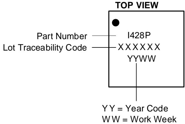
12 USE NOTES
12.1 ACCELEROMETER MODE TRANSITIONS
When transitioning from accelerometer Low Power (LP) mode to accelerometer Low Noise (LN) mode, if ODR is 6.25Hz or lower, software should change ODR to a value of 12.5Hz or higher, because accelerometer LN mode does not support ODR values below 12.5Hz.
When transitioning from accelerometer LN mode to accelerometer LP mode, if ODR is greater than 500Hz, software should change ODR to a value of 500Hz or lower, because accelerometer LP mode does not support ODR values above 500Hz.
12.2 ACCELEROMETER LOW POWER (LP) MODE AVERAGING FILTER SETTING
Software drivers provided with the device use Averaging Filter setting of 16x. This setting is recommended for meeting Android noise requirements in LP mode, and to minimize accelerometer offset variation when transitioning from LP to Low Noise (LN) mode 1x averaging filter can be used by following the setting configuration shown in section 14.38.
12.3 SETTINGS FOR I2C, I3CSM, AND SPI OPERATION
Upon bootup the device comes up in SPI mode. The following settings should be used for ${ | ^ {2 } C , | 3 C ^ { 5 \mathsf { M } } }$ , and SPI operation.
Scenario 1: INT1/INT2 pins are used for interrupt assertion in ${ | 3 C ^ { 5 M } }$ mode.
| Register Field | I2C Driver Setting | I3CSM Driver Setting | SPI Driver Setting |
| I3C_EN (bit 4, register INTF_CONFIG6, address 0x7C, bank 1) | 1 | 1 | 1 |
| I3C_SDR_EN (bit 0, register INTF_CONFIG6, address 0x7C, bank 1) | 0 | 1 | 1 |
| I3C_DDR_EN (bit 1, register INTF_CONFIG6, address 0x7C, bank 1) | 0 | 0 | 1 |
| I3C_BUS_MODE (bit 6, register INTF_CONFIG4, address 0x7A, bank 1) | 0 | 0 | 0 |
| I2C_SLEW_RATE (bits 5:3, register DRIVE_CONFIG, address 0x13, bank 0) | 1 | 0 | 0 |
| SPI_SLEW_RATE (bits 2:0, register DRIVE_CONFIG, address 0x13, bank 0) | 1 | 5 | 5 |
Scenario 2: IBI is used for interrupt assertion in ${ | 3 C ^ { \mathsf { S M } } }$ mode.
| Register Field | I2C Driver Setting | I3CSM Driver Setting | SPI Driver Setting |
| I3C_EN (bit 4, register INTF_CONFIG6, address 0x7C, bank 1) | 1 | 1 | 1 |
| I3C_SDR_EN (bit 0, register INTF_CONFIG6, address 0x7C, bank 1) | 0 | 1 | 1 |
| I3C_DDR_EN (bit 1, register INTF_CONFIG6, address 0x7C, bank 1) | 0 | 1 | 1 |
| I3C_BUS_MODE (bit 6, register INTF_CONFIG4, address 0x7A, bank 1) | 0 | 0 | 0 |
| I2C_SLEW_RATE (bits 5:3, register DRIVE_CONFIG, address 0x13, bank 0) | 1 | 0 | 0 |
| SPI_SLEW_RATE (bits 2:0, register DRIVE_CONFIG, address 0x13, bank 0) | 1 | 5 | 5 |
12.4 NOTCH FILTER AND ANTI-ALIAS FILTER OPERATION
Use of Notch Filter and Anti-Alias Filter is supported only for Low Noise (LN) mode operation. The host is responsible for keeping the UI path in LN mode while Notch Filter and Anti-Alias Filter are turned on.
12.5 EXTERNAL CLOCK INPUT EFFECT ON ODR
ODR values supported by the device scale with external clock frequency, if external clock input is used. The ODR values shown in the datasheet are supported with external clock input frequency of 32kHz. For any other external clock input frequency, these ODR values will scale by a factor of (External clock value in kHz / 32). For example, if an external clock frequency of 32.768kHz is used, instead of ODR value of 500Hz, it will be 500 * (32.768 / 32) = 512Hz.
12.6 INT_ASYNC_RESET CONFIGURATION
For register INT_CONFIG1 (bank 0 register 0x64) bit 4 INT_ASYNC_RESET, user should change setting to 0 from default setting of 1, for proper INT1 and INT2 pin operation.
12.7 FIFO TIMESTAMP INTERVAL SCALING
When RTC_MODE =1 (bank 0 register 0x4D bit2) and register INTF_CONFIG5 (bank 1 register 0x7B) bit 2:1 (PIN9_FUNCTION) is set to 10 for CLKIN input;
THEN
If TMST_RES = 0 (corresponding to timestamp resolution of 1µs), timestamp interval reported in FIFO requires scaling by a factor of 32.768/RTC Frequency.
For example when ODR = 1kHz, RTC Frequency 32kHz, the true timestamp interval should be 1000μs. But the value in FIFO toggles between 976 and 977. After scaling 976.5 * 32.768/32 = 1000μs.
If TMST_RES = 1 (corresponding to timestamp resolution of 1 RTC clock period), timestamp interval reported in FIFO requires scaling by a factor of RTC clock period.
For example when ODR = 1kHz, RTC Frequency 32kHz, the true timestamp interval should be 1000μs. But the value in FIFO is 32. After scaling 1/32kHz*32 = 1000μs.
ELSE
If TMST_RES = 0 (corresponding to timestamp resolution of 1µs), timestamp interval reported in FIFO requires scaling by a factor of 32/30.
For example when ODR = 1kHz, the true timestamp interval should be 1000μs. But the value in FIFO toggles between 937 and 938. After scaling 937.5 * 32/30 = 1000μs.
If TMST_RES = 1 (corresponding to timestamp resolution of 16µs), timestamp interval reported in FIFO requires scaling by a factor of 16*32/30.
For example when ODR = 1kHz, the true timestamp interval should be 1000μs. But the value in FIFO toggles between 58 and 59. After scaling 58.5 * 16* 32/30 = 1000μs.
12.8 SUPPLEMENTARY INFORMATION FOR FIFO_HOLD_LAST_DATA_EN
This section contains supplementary information for using register field FIFO_HOLD_LAST_DATA_EN (bit 7) of register INTF_CONFIG0 (address 0x4C, bank 0) .
The following table shows the values in FIFO:
| FIFO_HOLD_LAST_DATA_EN | 16-bit FIFO Packet | 20-bit FIFO Packet | |
| 0 (Insert Invalid code) | Valid sample | All values in: {-32766 to +32767} | Gyro: All Even numbers in {-524256 to +524286}Example: {-524256, -524254, -524252, -524250 .....+524284, +524286} |
| Accel: Every Other Even number in {-524256 to +524284}Example: {-524256, -524252, -524248, -524244 .....+524280, +524284} | |||
| Invalid sample | -32768 | -524288 | |
| 1 ("copy last valid" mode: No invalid code insertion) | Valid sample | All values in: {-32768 to +32767} | Gyro: All Even numbers in {-524288 to +524286}Example: {-524288, -524286, -524284, -524282 .....+524284, +524286} |
| Accel: Every Other Even number in {-524288 to +524284}Example: {-524288, -524284, -524280 .....+524280, +524284} | |||
| Invalid sample | Copy last valid sample | ||
Document Number: DS-000347 Revision: 1.9
The following table shows the values in sense registers on reset:
| FIFO_HOLD_LAST_DATA_EN = 0 | FIFO_HOLD_LAST_DATA_EN = 1 | |
| Power On Reset till First Sample | Accel/Gyro/Temperature Sensor = -32768 | Accel/Gyro/Temperature Sensor = 0 |
The following table shows the values in sense registers after first sample is received. As shown in table, the combination of FIFO_HOLD_LAST_DATA_EN and FSYNC Tag determine the range of values read for valid samples and invalid samples.
| FIFO_HOLD_LAST_DATA_EN | FSYNC tag disabled | FSYNC Enabled on one Sensor | |||
| Sensor selected for FSYNC Tag | Other Sensor Not selected for FSYNC tagging | ||||
| FSYNC tagged | FSYNC not tagged | ||||
| 0 (Insert Invalid code) | Valid sample | All values in: {-32766 to +32767} | All ODD values in: {-32765 to +32767} | All EVEN values in: {-32766 to +32766} | All values in: {-32766 to +32767} |
| Invalid sample | Registers do not receive invalid samples. Registers hold last valid sample until new one arrives | ||||
| 1 ("copy last valid" mode: No invalid code insertion) | Valid sample | All values in: {-32768 to +32767} | All ODD values in: {-32767 to +32767} | All EVEN values in: {-32768 to +32766} | All values in: {-32768 to +32767} |
| Invalid sample | Registers do not receive invalid samples. Registers hold last valid sample until new one arrives | ||||
12.9 REGISTER VALUES MODIFICATION
The only register settings that user can modify during sensor operation are for ODR selection, FSR selection, and sensor mode changes (register parameters GYRO_ODR, ACCEL_ODR, GYRO_FS_SEL, ACCEL_FS_SEL, GYRO_MODE, ACCEL_MODE). User must not modify any other register values during sensor operation. The following procedure must be used for other register values modification.
• Turn Accel and Gyro Off
• Modify register values
• Turn Accel and/or Gyro On
13 REGISTER MAP
This section lists the register map for the ICM-42688-P, for user banks 0, 1, 2, 3, 4.
13.1 USER BANK 0 REGISTER MAP
| Addr (Hex) | Addr (Dec.) | Register Name | Serial I/F | Bit7 | Bit6 | Bit5 | Bit4 | Bit3 | Bit2 | Bit1 | Bit0 |
| 11 | 17 | DEVICE_CONFIG | R/W | - | SPI_MODE | - | SOFT_RESET_CONFIG | ||||
| 13 | 19 | DRIVE_CONFIG | R/W | - | I2C_SLEW_RATE | SPI_SLEW_RATE | |||||
| 14 | 20 | INT_CONFIG | - | INT2_MODE | INT2_DRIVE_CIRCUIT | INT2_POLARITY | INT1_MODE | INT1_DRIVE_CIRCUIT | INT1_POLARITY | ||
| 16 | 22 | FIFO_CONFIG | R/W | FIFO_MODE | - | ||||||
| 1D | 29 | TEMP_DATA1 | SYNCR | TEMP_DATA[15:8] | |||||||
| 1E | 30 | TEMP_DATA0 | SYNCR | TEMP_DATA[7:0] | |||||||
| 1F | 31 | ACCEL_DATA_X1 | SYNCR | ACCEL_DATA_X[15:8] | |||||||
| 20 | 32 | ACCEL_DATA_X0 | SYNCR | ACCEL_DATA_X[7:0] | |||||||
| 21 | 33 | ACCEL_DATA_Y1 | SYNCR | ACCEL_DATA_Y[15:8] | |||||||
| 22 | 34 | ACCEL_DATA_Y0 | SYNCR | ACCEL_DATA_Y[7:0] | |||||||
| 23 | 35 | ACCEL_DATA_Z1 | SYNCR | ACCEL_DATA_Z[15:8] | |||||||
| 24 | 36 | ACCEL_DATA_Z0 | SYNCR | ACCEL_DATA_Z[7:0] | |||||||
| 25 | 37 | GYRO_DATA_X1 | SYNCR | GYRO_DATA_X[15:8] | |||||||
| 26 | 38 | GYRO_DATA_X0 | SYNCR | GYRO_DATA_X[7:0] | |||||||
| 27 | 39 | GYRO_DATA_Y1 | SYNCR | GYRO_DATA_Y[15:8] | |||||||
| 28 | 40 | GYRO_DATA_Y0 | SYNCR | GYRO_DATA_Y[7:0] | |||||||
| 29 | 41 | GYRO_DATA_Z1 | SYNCR | GYRO_DATA_Z[15:8] | |||||||
| 2A | 42 | GYRO_DATA_Z0 | SYNCR | GYRO_DATA_Z[7:0] | |||||||
| 2B | 43 | TMST_FSYNCH | SYNCR | TMST_FSYNC_DATA[15:8] | |||||||
| 2C | 44 | TMST_FSYNCL | SYNCR | TMST_FSYNC_DATA[7:0] | |||||||
| 2D | 45 | INT_STATUS | R/C | - | UI_FSYNC_INT | PLL_RDY_INT | RESET_DONE_INT | DATA_RDY_INT | FIFO_THS_INT | FIFO_FULL_INT | AGC_RDY_INT |
| 2E | 46 | FIFO_COUNTH | R | FIFO_COUNT[15:8] | |||||||
| 2F | 47 | FIFO_COUNTL | R | FIFO_COUNT[7:0] | |||||||
| 30 | 48 | FIFO_DATA | R | FIFO_DATA | |||||||
| 31 | 49 | APEX_DATA0 | SYNCR | STEP_CNT[7:0] | |||||||
| 32 | 50 | APEX_DATA1 | SYNCR | STEP_CNT[15:8] | |||||||
| 33 | 51 | APEX_DATA2 | R | STEP_CADENCE | |||||||
| 34 | 52 | APEX_DATA3 | R | - | DMP_IDLE | ACTIVITY_CLASS | |||||
| 35 | 53 | APEX_DATA4 | R | - | TAP_NUM | TAP_AXIS | TAP_DIR | ||||
| 36 | 54 | APEX_DATA5 | R | - | DOUBLE_TAP_TIMING | ||||||
| 37 | 55 | INT_STATUS2 | R/C | - | SMD_INT | WOM_Z_INT | WOM_Y_INT | WOM_X_INT | |||
| 38 | 56 | INT_STATUS3 | R/C | - | STEP_DET_INT | STEP_CNT_OVF_INT | TILT_DET_INT | - | TAP_DET_INT | ||
| 4B | 75 | SIGNAL_PATH_RESET | W/C | - | DMP_INIT_EN | DMP_MEM_RESET_EN | - | ABORT_AND_RESET | TMST_STROBE | FIFO_FLUSH | - |
| 4C | 76 | INTF_CONFIG0 | R/W | FIFO_HOLD_LAST_DATA_EN | FIFO_COUNT_REC | FIFO_COUNT_ENDIAN | SENSOR_DATA_ENDIAN | - | UI_SIFS_CFG | ||
| 4D | 77 | INTF_CONFIG1 | R/W | - | ACCEL_LP_CLK_SEL | RTC_MODE | CLKSEL | ||||
| 4E | 78 | PWR_MGMT0 | R/W | - | TEMP_DIS | IDLE | GYRO_MODE | ACCEL_MODE | |||
| 4F | 79 | GYRO_CONFIG0 | R/W | GYRO_FS_SEL | - | GYRO_ODR | |||||
| 50 | 80 | ACCEL_CONFIG0 | R/W | ACCEL_FS_SEL | - | ACCEL_ODR | |||||
| 51 | 81 | GYRO_CONFIG1 | R/W | TEMP_FILT_BW | - | GYRO_UI_FILT_ORD | GYRO_DEC2_M2_ORD | ||||
| 52 | 82 | GYRO_ACCEL_CONFIG0 | R/W | ACCEL_UI_FILT_BW | GYRO_UI_FILT_BW | ||||||
| 53 | 83 | ACCEL_CONFIG1 | R/W | - | ACCEL_UI_FILT_ORD | ACCEL_DEC2_M2_ORD | - | ||||
| 54 | 84 | TMST_CONFIG | R/W | - | TMST_TO_REGS_EN | TMST_RES | TMST_DELTA_EN | TMST_FSYNC_EN | TMST_EN | ||
| 56 | 86 | APEX_CONFIG0 | R/W | DMP_POWER_SAVE | TAP_ENABLE | PED_ENABLE | TILT_ENABLE | - | DMP_ODR | ||
| 57 | 87 | SMD_CONFIG | R/W | - | WOM_INT_MODE | WOM_MODE | SMD_MODE | ||||
| 5F | 95 | FIFO_CONFIG1 | R/W | - | FIFO_RESUME_PARTIAL_RD | FIFO_WM_GT_TH | FIFO_HIRES_EN | FIFO_TMST_FSYNC_EN | FIFO_TEMP_EN | FIFO_GYRO_EN | FIFO_ACCEL_EN |
| 60 | 96 | FIFO_CONFIG2 | R/W | FIFO_WM[7:0] | |||||||
| 61 | 97 | FIFO_CONFIG3 | R/W | - | FIFO_WM[11:8] | ||||||
| 62 | 98 | FSYNC_CONFIG | R/W | - | FSYNC_UI_SEL | - | FSYNC_UI_FLAG_CLEAR_SEL | FSYNC_POLARITY | |||
| 63 | 99 | INT_CONFIG0 | R/W | - | UI_DRDY_INT_CLEAR | FIFO_THS_INT_CLEAR | FIFO_FULL_INT_CLEAR | ||||
| 64 | 100 | INT_CONFIG1 | R/W | - | INT_TPULSE_DURATION | INT_TDEASSE_RT_DISABLE | INT_ASYNC_RESET | - | |||
| 65 | 101 | INT_SOURCE0 | R/W | - | UI_FSYNC_INT1_EN | PLL_RDY_INT1_EN | RESET_DONE_INT1_EN | UI_DRDY_INT1_EN | FIFO_THS_INT1_EN | FIFO_FULL_INT1_EN | UI_AGC_RDY_INT1_EN |
| 66 | 102 | INT_SOURCE1 | R/W | - | I3C_PROTOCOL_ERROR_INT1_EN | - | SMD_INT1_EN | WOM_Z_INT1_EN | WOM_Y_INT1_EN | WOM_X_INT1_EN | |
| 68 | 104 | INT_SOURCE3 | R/W | - | UI_FSYNC_INT2_EN | PLL_RDY_INT2_EN | RESET_DONE_INT2_EN | UI_DRDY_INT2_EN | FIFO_THS_INT2_EN | FIFO_FULL_INT2_EN | UI_AGC_RDY_INT2_EN |
| 69 | 105 | INT_SOURCE4 | R/W | - | I3C_PROTOCOL_ERROR_INT2_EN | - | SMD_INT2_EN | WOM_Z_INT2_EN | WOM_Y_INT2_EN | WOM_X_INT2_EN | |
| 6C | 108 | FIFO_LOST_PKT0 | R | FIFO_LOST_PKT_CNT[15:8] | |||||||
| 6D | 109 | FIFO_LOST_PKT1 | R | FIFO_LOST_PKT_CNT[7:0] | |||||||
| 70 | 112 | SELF_TEST_CONFIG | R/W | ACCEL_ST_POWER | EN_AZ_ST | EN_AY_ST | EN_AX_ST | EN_GZ_ST | EN_GY_ST | EN_GX_ST | |
| 75 | 117 | WHO_AM_I | R | WHOAMI | |||||||
| 76 | 118 | REG_BANK_SEL | R/W | - | BANK_SEL | ||||||
13.2 USER BANK 1 REGISTER MAP
| Addr (Hex) | Addr (Dec.) | Register Name | Serial I/F | Bit7 | Bit6 | Bit5 | Bit4 | Bit3 | Bit2 | Bit1 | Bit0 |
| 03 | 03 | SENSOR_CONFIG0 | R/W | - | ZG_DISABLE | YG_DISABLE | XG_DISABLE | ZA_DISABLE | YA_DISABLE | XA_DISABLE | |
| 0B | 11 | GYRO_CONFIG_STATIC2 | R/W | - | GYRO_AAF_DIS | GYRO_NF_DIS | |||||
| 0C | 12 | GYRO_CONFIG_STATIC3 | R/W | - | GYRO_AAF_DELT | ||||||
| 0D | 13 | GYRO_CONFIG_STATIC4 | R/W | GYRO_AAF_DELTSQR[7:0] | |||||||
| 0E | 14 | GYRO_CONFIG_STATIC5 | R/W | GYRO_AAF_BITSHIFT | GYRO_AAF_DELTSQR[11:8] | ||||||
| 0F | 15 | GYRO_CONFIG_STATIC6 | R/W | GYRO_X_NF_COSWZ[7:0] | |||||||
| 10 | 16 | GYRO_CONFIG_STATIC7 | R/W | GYRO_Y_NF_COSWZ[7:0] | |||||||
| 11 | 17 | GYRO_CONFIG_STATIC8 | R/W | GYRO_Z_NF_COSWZ[7:0] | |||||||
| 12 | 18 | GYRO_CONFIG_STATIC9 | R/W | - | GYRO_Z_NF_COSWZ_SEL[0] | GYRO_Y_NF_COSWZ_SEL[0] | GYRO_X_NF_COSWZ_SEL[0] | GYRO_Z_NF_COSWZ[8] | GYRO_Y_NF_COSWZ[8] | GYRO_X_NF_COSWZ[8] | |
| 13 | 19 | GYRO_CONFIG_STATIC10 | R/W | - | GYRO_NF_BW_SEL | - | |||||
| 5F | 95 | XG_ST_DATA | R/W | XG_ST_DATA | |||||||
| 60 | 96 | YG_ST_DATA | R/W | YG_ST_DATA | |||||||
| 61 | 97 | ZG_ST_DATA | R/W | ZG_ST_DATA | |||||||
| 62 | 98 | TMSTVAL0 | R | TMST_VALUE[7:0] | |||||||
| 63 | 99 | TMSTVAL1 | R | TMST_VALUE[15:8] | |||||||
| 64 | 100 | TMSTVAL2 | R | - | TMST_VALUE[19:16] | ||||||
| 7A | 122 | INTF_CONFIG4 | R/W | - | I3C_BUS_MODE | - | SPI_AP_4WIRE | - | |||
| 7B | 123 | INTF_CONFIG5 | R/W | - | PIN9_FUNCTION | - | |||||
| 7C | 124 | INTF_CONFIG6 | R/W | ASYNCTIMEO_DIS | - | I3C_EN | I3C_IBI_BYTE_EN | I3C_IBI_EN | I3C_DDR_EN | I3C_SDR_EN | |
13.3 USER BANK 2 REGISTER MAP
| Addr (Hex) | Addr (Dec.) | Register Name | Serial I/F | Bit7 | Bit6 | Bit5 | Bit4 | Bit3 | Bit2 | Bit1 | Bit0 |
| 03 | 03 | ACCEL_CONFIG_STATIC2 | R/W | - | ACCEL_AAF_DELT | ACCEL_AAF_DIS | |||||
| 04 | 04 | ACCEL_CONFIG_STATIC3 | R/W | ACCEL_AAF_DELTSQR[7:0] | |||||||
| 05 | 05 | ACCEL_CONFIG_STATIC4 | R/W | ACCEL_AAF_BITSHIFT | ACCEL_AAF_DELTSQR[11:8] | ||||||
| 3B | 59 | XA_ST_DATA | R/W | XA_ST_DATA | |||||||
| 3C | 60 | YA_ST_DATA | R/W | YA_ST_DATA | |||||||
| 3D | 61 | ZA_ST_DATA | R/W | ZA_ST_DATA | |||||||
13.4 USER BANK 3 REGISTER MAP
| Addr (Hex) | Addr (Dec.) | Register Name | Serial I/F | Bit7 | Bit6 | Bit5 | Bit4 | Bit3 | Bit2 | Bit1 | Bit0 |
| 2A | 42 | CLKDIV | R | - | CLKDIV | ||||||
13.5 USER BANK 4 REGISTER MAP
| Addr (Hex) | Addr (Dec.) | Register Name | Serial I/F | Bit7 | Bit6 | Bit5 | Bit4 | Bit3 | Bit2 | Bit1 | Bit0 |
| 40 | 64 | APEX_CONFIG1 | R/W | LOW_ENERGY_AMP_TH_SEL | DMP_POWER_SAVE_TIME_SEL | ||||||
| 41 | 65 | APEX_CONFIG2 | R/W | PED_AMP_TH_SEL | PED_STEP_CNT_TH_SEL | ||||||
| 42 | 66 | APEX_CONFIG3 | R/W | PED_STEP_DET_TH_SEL | PED_SB_TIMER_TH_SEL | PED_HI_EN_TH_SEL | |||||
| 43 | 67 | APEX_CONFIG4 | R/W | TILT_WAIT_TIME_SEL | |||||||
| 46 | 70 | APEX_CONFIG7 | R/W | TAP_MIN_JERK_THR | TAP_MAX_PEAK_TOL | ||||||
| 47 | 71 | APEX_CONFIG8 | R/W | - | TAP_TMAX | TAP_TAVG | TAP_TMIN | ||||
| 48 | 72 | APEX_CONFIG9 | R/W | - | SENSITIVITY_MODE | ||||||
| 4A | 74 | ACCEL_WOM_X_THR | R/W | WOM_X_TH | |||||||
| 4B | 75 | ACCEL_WOM_Y_THR | R/W | WOM_Y_TH | |||||||
| 4C | 76 | ACCEL_WOM_Z_THR | R/W | WOM_Z_TH | |||||||
| 4D | 77 | INT_SOURCE6 | R/W | - | STEP_DET_INT1_EN | STEP_CNT_OFL_INT1_EN | TILT_DET_INT1_EN | - | TAP_DET_INT1_EN | ||
| 4E | 78 | INT_SOURCE7 | R/W | - | STEP_DET_INT2_EN | STEP_CNT_OFL_INT2_EN | TILT_DET_INT2_EN | - | TAP_DET_INT2_EN | ||
| 4F | 79 | INT_SOURCE8 | R/W | - | FSYNC_IBI_EN | PLL_RDY_IBI_EN | UI_DRDY_IBI_EN | FIFO_THS_IBI_EN | FIFO_FULL_IBI_EN | AGC_RDY_IBI_EN | |
| 50 | 80 | INT_SOURCE9 | R/W | I3C_PROTOCOL_ERROR_IBI_EN | - | SMD_IBI_EN | WOM_Z_IBI_EN | WOM_Y_IBI_EN | WOM_X_IBI_EN | - | |
| 51 | 81 | INT_SOURCE10 | R/W | - | STEP_DET_IBI_EN | STEP_CNT_OFL_IBI_EN | TILT_DET_IBI_EN | - | TAP_DET_IBI_EN | ||
| 77 | 119 | OFFSET_USER0 | R/W | GYRO_X_OFFUSER[7:0] | |||||||
| 78 | 120 | OFFSET_USER1 | R/W | GYRO_Y_OFFUSER[11:8] | GYRO_X_OFFUSER[11:8] | ||||||
| 79 | 121 | OFFSET_USER2 | R/W | GYRO_Y_OFFUSER[7:0]- | |||||||
| 7A | 122 | OFFSET_USER3 | R/W | GYRO_Z_OFFUSER[7:0] | |||||||
| 7B | 123 | OFFSET_USER4 | R/W | ACCEL_X_OFFUSER[11:8] | GYRO_Z_OFFUSER[11:8] | ||||||
| 7C | 124 | OFFSET_USER5 | R/W | ACCEL_X_OFFUSER[7:0] | |||||||
| 7D | 125 | OFFSET_USER6 | R/W | ACCEL_Y_OFFUSER[7:0] | |||||||
| 7E | 126 | OFFSET_USER7 | R/W | ACCEL_Z_OFFUSER[11:8] | ACCEL_Y_OFFUSER[11:8] | ||||||
| 7F | 127 | OFFSET_USER8 | R/W | ACCEL_Z_OFFUSER[7:0] | |||||||
Detailed register descriptions are provided in the sections that follow. Please note the following regarding Clock Domain for each register:
• Clock Domain: SCLK_UI means that the register is controlled from the UI interface
Register fields marked as Reserved must not be modified by the user. The Reset Value of the register can be used to determine the default value of reserved register fields, and unless otherwise noted this default value must be maintained even if the values of other register fields are modified by the user.
14 USER BANK 0 REGISTER MAP – DESCRIPTIONS
This section describes the function and contents of each register within USR Bank 0.
Note: The device powers up in sleep mode.
14.1 DEVICE_CONFIG
| Name: DEVICE_CONFIGAddress: 17 (11h)Serial IF: R/WReset value: 0x00Clock Domain: SCLK_UI | ||
| BIT | NAME | FUNCTION |
| 7:5 | - | Reserved |
| 4 | SPI_MODE | SPI mode selection0: Mode 0 and Mode 3 (default)1: Mode 1 and Mode 2 |
| 3:1 | - | Reserved |
| 0 | SOFT_RESET_CONFIG | Software reset configuration0: Normal (default)1: Enable resetAfter writing 1 to this bitfield, wait 1ms for soft reset to be effective, before attempting any other register access |
14.2 DRIVE_CONFIG
| Name: DRIVE_CONFIGAddress: 19 (13h)Serial IF: R/WReset value: 0x05Clock Domain: SCLK_UI | ||
| BIT | NAME | FUNCTION |
| 7:6 | - | Reserved |
| 5:3 | I2C_SLEW_RATE | Controls slew rate for output pin 14 in $I^{2}C$ mode only000: 20ns-60ns001: 12ns-36ns010: 6ns-18ns011: 4ns-12ns100: 2ns-6ns101: < 2ns110: Reserved111: Reserved |
| 2:0 | SPI_SLEW_RATE | Controls slew rate for output pin 14 in SPI or $I3C^{SM}$ mode, and for all other output pins000: 20ns-60ns001: 12ns-36ns010: 6ns-18ns011: 4ns-12ns100: 2ns-6ns101: < 2ns110: Reserved111: Reserved |
14.3 INT_CONFIG
| Name: INT_CONFIGAddress: 20 (14h)Serial IF: R/WReset value: 0x00Clock Domain: SCLK_UI | ||
| BIT | NAME | FUNCTION |
| 7:6 | - | Reserved |
| 5 | INT2_MODE | INT2 interrupt mode0: Pulsed mode1: Latched mode |
| 4 | INT2_DRIVE_CIRCUIT | INT2 drive circuit0: Open drain1: Push pull |
| 3 | INT2_POLARITY | INT2 interrupt polarity0: Active low (default)1: Active high |
| 2 | INT1_MODE | INT1 interrupt mode0: Pulsed mode1: Latched mode |
| 1 | INT1_DRIVE_CIRCUIT | INT1 drive circuit0: Open drain1: Push pull |
| 0 | INT1_POLARITY | INT1 interrupt polarity0: Active low (default)1: Active high |
14.4 FIFO_CONFIG
| Name: FIFO_CONFIGAddress: 22 (16h)Serial IF: R/WReset value: 0x00Clock Domain: SCLK_UI | ||
| BIT | NAME | FUNCTION |
| 7:6 | FIFO_MODE | 00: Bypass Mode (default)01: Stream-to-FIFO Mode10: STOP-on-FULL Mode11: STOP-on-FULL Mode |
| 5:0 | - | Reserved |
14.5 TEMP_DATA1
| Name: TEMP_DATA1Address: 29 (1Dh)Serial IF: SYNCRReset value: 0x80Clock Domain: SCLK_UI | ||
| BIT | NAME | FUNCTION |
| 7:0 | TEMP_DATA[15:8] | Upper byte of temperature data |
14.6 TEMP_DATA0
| Name: TEMP_DATA0Address: 30 (1Eh)Serial IF: SYNCRReset value: 0x00Clock Domain: SCLK_UI | ||
| BIT | NAME | FUNCTION |
| 7:0 | TEMP_DATA[7:0] | Lower byte of temperature data |
Temperature sensor register data TEMP_DATA is updated with new data at max(Accelerometer ODR, Gyroscope ODR).
Temperature data value from the sensor data registers can be converted to degrees centigrade by using the following formula:
Temperature in Degrees Centigrade = (TEMP_DATA / 132.48) + 25
Temperature data stored in FIFO is an 8-bit quantity, FIFO_TEMP_DATA. It can be converted to degrees centigrade by using the following formula:
Temperature in Degrees Centigrade = (FIFO_TEMP_DATA / 2.07) + 25
14.7 ACCEL_DATA_X1
| Name: ACCEL_DATA_X1Address: 31 (1Fh)Serial IF: SYNCRReset value: 0x80Clock Domain: SCLK_UI | ||
| BIT | NAME | FUNCTION |
| 7:0 | ACCEL_DATA_X[15:8] | Upper byte of Accel X-axis data |
14.8 ACCEL_DATA_X0
| Name: ACCEL_DATA_X0Address: 32 (20h)Serial IF: SYNCRReset value: 0x00Clock Domain: SCLK_UI | ||
| BIT | NAME | FUNCTION |
| 7:0 | ACCEL_DATA_X[7:0] | Lower byte of Accel X-axis data |
14.9 ACCEL_DATA_Y1
| Name: ACCEL_DATA_Y1Address: 33 (21h)Serial IF: SYNCRReset value: 0x80Clock Domain: SCLK_UI | ||
| BIT | NAME | FUNCTION |
| 7:0 | ACCEL_DATA_Y[15:8] | Upper byte of Accel Y-axis data |
14.10 ACCEL_DATA_Y0
| Name: ACCEL_DATA_Y0Address: 34 (22h)Serial IF: SYNCRReset value: 0x00Clock Domain: SCLK_UI | ||
| BIT | NAME | FUNCTION |
| 7:0 | ACCEL_DATA_Y[7:0] | Lower byte of Accel Y-axis data |
14.11 ACCEL_DATA_Z1
| Name: ACCEL_DATA_Z1Address: 35 (23h)Serial IF: SYNCRReset value: 0x80Clock Domain: SCLK_UI | ||
| BIT | NAME | FUNCTION |
| 7:0 | ACCEL_DATA_Z[15:8] | Upper byte of Accel Z-axis data |
14.12 ACCEL_DATA_Z0
| Name: ACCEL_DATA_Z0Address: 36 (24h)Serial IF: SYNCRReset value: 0x00Clock Domain: SCLK_UI | ||
| BIT | NAME | FUNCTION |
| 7:0 | ACCEL_DATA_Z[7:0] | Lower byte of Accel Z-axis data |
14.13 GYRO_DATA_X1
| Name: GYRO_DATA_X1Address: 37 (25h)Serial IF: SYNCRReset value: 0x80Clock Domain: SCLK_UI | ||
| BIT | NAME | FUNCTION |
| 7:0 | GYRO_DATA_X[15:8] | Upper byte of Gyro X-axis data |
14.14 GYRO_DATA_X0
| Name: GYRO_DATA_X0Address: 38 (26h)Serial IF: SYNCRReset value: 0x00Clock Domain: SCLK_UI | ||
| BIT | NAME | FUNCTION |
| 7:0 | GYRO_DATA_X[7:0] | Lower byte of Gyro X-axis data |
14.15 GYRO_DATA_Y1
| Name: GYRO_DATA_Y1Address: 39 (27h)Serial IF: SYNCRReset value: 0x80Clock Domain: SCLK_UI | ||
| BIT | NAME | FUNCTION |
| 7:0 | GYRO_DATA_Y[15:8] | Upper byte of Gyro Y-axis data |
14.16 GYRO_DATA_Y0
| Name: GYRO_DATA_Y0Address: 40 (28h)Serial IF: SYNCRReset value: 0x00Clock Domain: SCLK_UI | ||
| BIT | NAME | FUNCTION |
| 7:0 | GYRO_DATA_Y[7:0] | Lower byte of Gyro Y-axis data |
14.17 GYRO_DATA_Z1
| Name: GYRO_DATA_Z1Address: 41 (29h)Serial IF: SYNCRReset value: 0x80Clock Domain: SCLK_UI | ||
| BIT | NAME | FUNCTION |
| 7:0 | GYRO_DATA_Z[15:8] | Upper byte of Gyro Z-axis data |
14.18 GYRO_DATA_Z0
| Name: GYRO_DATA_Z0Address: 42 (2Ah)Serial IF: SYNCRReset value: 0x00Clock Domain: SCLK_UI | ||
| BIT | NAME | FUNCTION |
| 7:0 | GYRO_DATA_Z[7:0] | Lower byte of Gyro Z-axis data |
14.19 TMST_FSYNCH
| Name: TMST_FSYNCHAddress: 43 (2Bh)Serial IF: SYNCRReset value: 0x00Clock Domain: SCLK_UI | ||
| BIT | NAME | FUNCTION |
| 7:0 | TMST_FSYNC_DATA_UI[15:8] | Stores the upper byte of the time delta from the rising edge of FSYNC to the latest ODR until the UI Interface reads the FSYNC tag in the status register |
14.20 TMST_FSYNCL
| Name: TMST_FSYNCLAddress: 44 (2Ch)Serial IF: SYNCRReset value: 0x00Clock Domain: SCLK_UI | ||
| BIT | NAME | FUNCTION |
| 7:0 | TMST_FSYNC_DATA_UI[7:0] | Stores the lower byte of the time delta from the rising edge of FSYNC to the latest ODR until the UI Interface reads the FSYNC tag in the status register |
14.21 INT_STATUS
| Name: INT_STATUSAddress: 45 (2Dh)Serial IF: R/CReset value: 0x10Clock Domain: SCLK_UI | ||
| BIT | NAME | FUNCTION |
| 7 | - | Reserved |
| 6 | UI_FSYNC_INT | This bit automatically sets to 1 when a UI FSYNC interrupt is generated. The bit clears to 0 after the register has been read. |
| 5 | PLL_RDY_INT | This bit automatically sets to 1 when a PLL Ready interrupt is generated. The bit clears to 0 after the register has been read. |
| 4 | RESET_DONE_INT | This bit automatically sets to 1 when software reset is complete. The bit clears to 0 after the register has been read. |
| 3 | DATA_RDY_INT | This bit automatically sets to 1 when a Data Ready interrupt is generated. The bit clears to 0 after the register has been read. |
| 2 | FIFO_THS_INT | This bit automatically sets to 1 when the FIFO buffer reaches the threshold value. The bit clears to 0 after the register has been read. |
| 1 | FIFO_FULL_INT | This bit automatically sets to 1 when the FIFO buffer is full. The bit clears to 0 after the register has been read. |
| 0 | AGC_RDY_INT | This bit automatically sets to 1 when an AGC Ready interrupt is generated. The bit clears to 0 after the register has been read. |
14.22 FIFO_COUNTH
| Name: FIFO_COUNTHAddress: 46 (2Eh)Serial IF: RReset value: 0x00Clock Domain: SCLK_UI | ||
| BIT | NAME | FUNCTION |
| 7:0 | FIFO_COUNT[15:8] | High Bits, count indicates the number of records or bytes available in FIFO according to FIFO_COUNT_REC setting.Reading this byte latches the data for both FIFO_COUNTH, and FIFO_COUNTL. |
14.23 FIFO_COUNTL
| Name: FIFO_COUNTLAddress: 47 (2Fh)Serial IF: RReset value: 0x00Clock Domain: SCLK_UI | ||
| BIT | NAME | FUNCTION |
| 7:0 | FIFO_COUNT[7:0] | Low Bits, count indicates the number of records or bytes available in FIFO according to FIFO_COUNT_REC setting.Note: Must read FIFO_COUNTH to latch new data for both FIFO_COUNTH and FIFO_COUNTL. |
14.24 FIFO_DATA
| Name: FIFO_DATAAddress: 48 (30h)Serial IF: RReset value: 0xFFClock Domain: SCLK_UI | ||
| BIT | NAME | FUNCTION |
| 7:0 | FIFO_DATA | FIFO data port |
14.25 APEX_DATA0
| Name: APEX_DATA0Address: 49 (31h)Serial IF: SYNCRReset value: 0x00Clock Domain: SCLK_UI | ||
| BIT | NAME | FUNCTION |
| 7:0 | STEP_CNT[7:0] | Pedometer Output: Lower byte of Step Count measured by pedometer |
14.26 APEX_DATA1
| Name: APEX_DATA1Address: 50 (32h)Serial IF: SYNCRReset value: 0x00Clock Domain: SCLK_UI | ||
| BIT | NAME | FUNCTION |
| 7:0 | STEP_CNT[15:8] | Pedometer Output: Upper byte of Step Count measured by pedometer |
14.27 APEX_DATA2
| Name: APEX_DATA2Address: 51 (33h)Serial IF: RReset value: 0x00Clock Domain: SCLK_UI | ||
| BIT | NAME | FUNCTION |
| 7:0 | STEP_CADENCE | Pedometer Output: Walk/run cadency in number of samples. Format is u6.2. e.g. At 50Hz ODR and 2Hz walk frequency, the cadency is 25 samples. The register will output 100. |
14.28 APEX_DATA3
| Name: APEX_DATA3Address: 52 (34h)Serial IF: RReset value: 0x04Clock Domain: SCLK_UI | ||
| BIT | NAME | FUNCTION |
| 7:3 | - | Reserved |
| 2 | DMP_IDLE | 0: Indicates DMP is running1: Indicates DMP is idle |
| 1:0 | ACTIVITY_CLASS | Pedometer Output: Detected activity00: Unknown01: Walk10: Run11: Reserved |
14.29 APEX_DATA4
| Name: APEX_DATA4Address: 53 (35h)Serial IF: RReset value: 0x00Clock Domain: SCLK_UI | ||
| BIT | NAME | FUNCTION |
| 7:5 | - | Reserved |
| 4:3 | TAP_NUM | Tap Detection Output: Number of taps in the current Tap event00: No tap01: Single tap10: Double tap11: Reserved |
| 2:1 | TAP_AXIS | Tap Detection Output: Represents the accelerometer axis on which tap energy is concentrated00: X-axis01: Y-axis10: Z-axis11: Reserved |
| 0 | TAP_DIR | Tap Detection Output: Polarity of tap pulse0: Current accelerometer value – Previous accelerometer value is a positive value1: Current accelerometer value – Previous accelerometer value is a negative value or zero |
14.30 APEX_DATA5
| Name: APEX_DATA5Address: 54 (36h)Serial IF: RReset value: 0x00Clock Domain: SCLK_UI | ||
| BIT | NAME | FUNCTION |
| 7:6 | - | Reserved |
| 5:0 | DOUBLE_TAP_TIMING | DOUBLE_TAP_TIMING measures the time interval between the two taps when double tap is detected. It counts every 16 accelerometer samples as one unit between the 2 tap pulses. Therefore, the value is related to the accelerometer ODR.Time in seconds = DOUBLE_TAP_TIMING * 16 / ODRFor example, if the accelerometer ODR is 500 Hz, and the DOUBLE_TAP_TIMING register reading is 6, the time interval value is 6*16/500 = 0.192 seconds. |
14.31 INT_STATUS2
| Name: INT_STATUS2Address: 55 (37h)Serial IF: R/CReset value: 0x00Clock Domain: SCLK_UI | ||
| BIT | NAME | FUNCTION |
| 7:4 | - | Reserved |
| 3 | SMD_INT | Significant Motion Detection Interrupt, clears on read |
| 2 | WOM_Z_INT | Wake on Motion Interrupt on Z-axis, clears on read |
| 1 | WOM_Y_INT | Wake on Motion Interrupt on Y-axis, clears on read |
| 0 | WOM_X_INT | Wake on Motion Interrupt on X-axis, clears on read |
14.32 INT_STATUS3
| Name: INT_STATUS3Address: 56 (38h)Serial IF: R/CReset value: 0x00Clock Domain: SCLK_UI | ||
| BIT | NAME | FUNCTION |
| 7:6 | - | Reserved |
| 5 | STEP_DET_INT | Step Detection Interrupt, clears on read |
| 4 | STEP_CNT_OVF_INT | Step Count Overflow Interrupt, clears on read |
| 3 | TILT_DET_INT | Tilt Detection Interrupt, clears on read |
| 2:1 | - | Reserved |
| 0 | TAP_DET_INT | Tap Detection Interrupt, clears on read |
14.33 SIGNAL_PATH_RESET
| Name: SIGNAL_PATH_RESETAddress: 75 (4Bh)Serial IF: W/CReset value: 0x00Clock Domain: SCLK_UI | ||
| BIT | NAME | FUNCTION |
| 7 | - | Reserved |
| 6 | DMP_INIT_EN | When this bit is set to 1, the DMP is enabled |
| 5 | DMP_MEM_RESET_EN | When this bit is set to 1, the DMP memory is reset |
| 4 | - | Reserved |
| 3 | ABORT_AND_RESET | When this bit is set to 1, the signal path is reset by restarting the ODR counter and signal path controls |
| 2 | TMST_STROBE | When this bit is set to 1, the time stamp counter is latched into the time stamp register. This is a write on clear bit. |
| 1 | FIFO_FLUSH | When set to 1, FIFO will get flushed. |
| 0 | - | Reserved |
14.34 INTF_CONFIG0
| Name: INTF_CONFIG0Address: 76 (4Ch)Serial IF: R/WReset value: 0x30Clock Domain: SCLK_UI | ||
| BIT | NAME | FUNCTION |
| 7 | FIFO_HOLD_LAST_DATA_EN | This bit selects the treatment of invalid samples. SeeInvalid Data Generationnote below this register description.Setting this bit to 0:In order to signal an invalid sample, and to differentiate it from a valid sample based on values only:Sense Registers:Do not receive invalid samples. They hold the last valid sample. Repeated reading before new sample received will yield copies of the last valid sample.Valid samples of values -32768, -32767 are replaced with -32766FSYNC Tagging can modify the least significant bit and further limit values (see section 12.8).FIFO:16-bit FIFO packet: Same as Sense Registers, except:OSYNC tagging is not applied to data in FIFO.20-bit FIFO packet:Invalid samples are indicated with the value -524288Valid samples in {-524288 to -524258} are replaced by -524256Valid Gyro samples: All Even numbers in {-524256 to +524286}Valid Accel samples: All numbers divisible by 4 in {-524256 to +524284}FSYNC tagging is not applied to data in FIFO.Setting this bit to 1:Sense registers:Do not receive invalid samples. They hold the last valid sample. Repeated reading before new sample received will yield copies of the last valid sample.FSYNC Tagging can modify the least significant bit and further limit values (see section 12.8).FIFO:Invalid sample will get copy of last valid sample16-bit FIFO packet: Same as Sense Registers, except:OSYNC tagging is not applied to data in FIFO.20-bit FIFO packet:Valid Gyro samples: All Even numbers in {-524288 to +524286}- Valid Accel samples: All numbers divisible by 4 in {-524288 to +524284}FSYNC tagging is not applied to data in FIFO. |
| 6 | FIFO_COUNT_REC | 0: FIFO count is reported in bytes1: FIFO count is reported in records (1 record = 16 bytes for header + gyro + accel + temp sensor data + time stamp, or 8 bytes for header + gyro/accel + temp sensor data, or 20 bytes for header + gyro + accel + temp sensor data + time stamp + 20-bit extension data) |
| 5 | FIFO_COUNT_ENDIAN | 0: FIFO count is reported in Little Endian format1: FIFO count is reported in Big Endian format (default) |
| 4 | SENSOR_DATA_ENDIAN | 0: Sensor data is reported in Little Endian format1: Sensor data is reported in Big Endian format (default) |
| 3:2 | - | Reserved |
| 1:0 | UI_SIFS_CFG | 0x: Reserved10: Disable SPI11: Disable I2C |
Invalid Data Generation: FIFO/Sense Registers may contain invalid data under the following conditions:
a) From power on reset to first ODR sample of any sensor (accel, gyro, temp sensor)
b) When any sensor is disabled (accel, gyro, temp sensor)
c) When accel and gyro are enabled with different ODRs. In this case, the sensor with lower ODR will generate invalid samples when it has no new data.
Invalid data can take special values or can hold last valid sample received. For -32768 to be used as a flag for invalid accel/gyro samples, the valid accel/gyro sample range is limited in such case as well. Bit 7 of INTF_CONFIG0 controls what values invalid (and valid) samples can take as shown above.
14.35 INTF_CONFIG1
| Name: INTF_CONFIG1Address: 77 (4Dh)Serial IF: R/WReset value: 0x91Clock Domain: SCLK_UI | ||
| BIT | NAME | FUNCTION |
| 7:4 | - | Reserved |
| 3 | ACCEL_LP_CLK_SEL | 0: Accelerometer LP mode uses Wake Up oscillator clock1: Accelerometer LP mode uses RC oscillator clock |
| 2 | RTC_MODE | 0: No input RTC clock is required1: RTC clock input is required |
| 1:0 | CLKSEL | 00: Always select internal RC oscillator01: Select PLL when available, else select RC oscillator (default)10: Reserved11: Disable all clocks |
14.36 PWR_MGMT0
| Name: PWR_MGMT0Address: 78 (4Eh)Serial IF: R/WReset value: 0x00Clock Domain: SCLK_UI | ||
| BIT | NAME | FUNCTION |
| 7:6 | - | Reserved |
| 5 | TEMP_DIS | 0: Temperature sensor is enabled (default)1: Temperature sensor is disabled |
| 4 | IDLE | If this bit is set to 1, the RC oscillator is powered on even if Accel and Gyro are powered off.Nominally this bit is set to 0, so when Accel and Gyro are powered off,the chip will go to OFF state, since the RC oscillator will also be powered off |
| 3:2 | GYRO_MODE | 00: Turns gyroscope off (default)01: Places gyroscope in Standby Mode10: Reserved11: Places gyroscope in Low Noise (LN) ModeGyroscope needs to be kept ON for a minimum of 45ms. When transitioning from OFF to any of the other modes, do not issue any register writes for 200μs. |
| 1:0 | ACCEL_MODE | 00: Turns accelerometer off (default)01: Turns accelerometer off10: Places accelerometer in Low Power (LP) Mode11: Places accelerometer in Low Noise (LN) ModeWhen transitioning from OFF to any of the other modes, do not issue any register writes for 200μs. |
14.37 GYRO_CONFIG0
| Name: GYRO_CONFIG0Address: 79 (4Fh)Serial IF: R/WReset value: 0x06Clock Domain: SCLK_UI | ||
| BIT | NAME | FUNCTION |
| 7:5 | GYRO_FS_SEL | Full scale select for gyroscope UI interface output000: ±2000dps (default)001: ±1000dps010: ±500dps011: ±250dps100: ±125dps101: ±62.5dps110: ±31.25dps111: ±15.625dps |
| 4 | - | Reserved |
| 3:0 | GYRO_ODR | Gyroscope ODR selection for UI interface output0000: Reserved0001: 32kHz0010: 16kHz0011: 8kHz0100: 4kHz0101: 2kHz0110: 1kHz (default)0111: 200Hz1000: 100Hz1001: 50Hz1010: 25Hz1011: 12.5Hz1100: Reserved1101: Reserved1110: Reserved1111: 500Hz |
14.38 ACCEL_CONFIG0
| Name: ACCEL_CONFIG0Address: 80 (50h)Serial IF: R/WReset value: 0x06Clock Domain: SCLK_UI | ||
| BIT | NAME | FUNCTION |
| 7:5 | ACCEL_FS_SEL | Full scale select for accelerometer UI interface output000: ±16g (default)001: ±8g010: ±4g011: ±2g100: Reserved101: Reserved110: Reserved111: Reserved |
| 4 | - | Reserved |
| 3:0 | ACCEL_ODR | Accelerometer ODR selection for UI interface output0000: Reserved0001: 32kHz (LN mode)0010: 16kHz (LN mode)0011: 8kHz (LN mode)0100: 4kHz (LN mode)0101: 2kHz (LN mode)0110: 1kHz (LN mode) (default)0111: 200Hz (LP or LN mode)1000: 100Hz (LP or LN mode)1001: 50Hz (LP or LN mode)1010: 25Hz (LP or LN mode)1011: 12.5Hz (LP or LN mode)1100: 6.25Hz (LP mode)1101: 3.125Hz (LP mode)1110: 1.5625Hz (LP mode)1111: 500Hz (LP or LN mode) |
14.39 GYRO_CONFIG1
| Name: GYRO_CONFIG1Address: 81 (51h)Serial IF: R/WReset value: 0x16Clock Domain: SCLK_UI | ||
| BIT | NAME | FUNCTION |
| 7:5 | TEMP_FILT_BW | Sets the bandwidth of the temperature signal DLPF000: DLPF BW = 4000Hz; DLPF Latency = 0.125ms (default)001: DLPF BW = 170Hz; DLPF Latency = 1ms010: DLPF BW = 82Hz; DLPF Latency = 2ms011: DLPF BW = 40Hz; DLPF Latency = 4ms100: DLPF BW = 20Hz; DLPF Latency = 8ms101: DLPF BW = 10Hz; DLPF Latency = 16ms110: DLPF BW = 5Hz; DLPF Latency = 32ms111: DLPF BW = 5Hz; DLPF Latency = 32ms |
| 4 | - | Reserved |
| 3:2 | GYRO_UI_FILT_ORD | Selects order of GYRO UI filter00: $1^{st}$ Order01: $2^{nd}$ Order10: $3^{rd}$ Order11: Reserved |
| 1:0 | GYRO_DEC2_M2_ORD | Selects order of GYRO DEC2_M2 Filter00: Reserved01: Reserved10: $3^{rd}$ Order11: Reserved |
14.40 GYRO_ACCEL_CONFIG0
| Name: GYRO_ACCEL_CONFIG0Address: 82 (52h)Serial IF: R/WReset value: 0x11Clock Domain: SCLK_UI | ||
| BIT | NAME | FUNCTION |
| 7:4 | ACCEL_UI_FILT_BW | LN Mode:Bandwidth for Accel LPF0 BW=ODR/21 BW=max(400Hz, ODR)/4 (default)2 BW=max(400Hz, ODR)/53 BW=max(400Hz, ODR)/84 BW=max(400Hz, ODR)/105 BW=max(400Hz, ODR)/166 BW=max(400Hz, ODR)/207 BW=max(400Hz, ODR)/408 to 13: Reserved14 Low Latency option: Trivial decimation @ ODR of Dec2 filter output. Dec2 runs at max(400Hz, ODR)15 Low Latency option: Trivial decimation @ ODR of Dec2 filter output. Dec2 runs at max(200Hz, 8*ODR)LP Mode:0 Reserved1 1x AVG filter (default)2 to 5 Reserved6 16x AVG filter7 to 15 Reserved |
| 3:0 | GYRO_UI_FILT_BW | LN Mode:Bandwidth for Gyro LPF0 BW=ODR/21 BW=max(400Hz, ODR)/4 (default)2 BW=max(400Hz, ODR)/53 BW=max(400Hz, ODR)/84 BW=max(400Hz, ODR)/105 BW=max(400Hz, ODR)/166 BW=max(400Hz, ODR)/207 BW=max(40OHz, ODR)/408 to 13: Reserved14 Low Latency option: Trivial decimation @ ODR of Dec2 filter output. Dec2 runs at max(400Hz, ODR)15 Low Latency option: Trivial decimation @ ODR of Dec2 filter output. Dec2 runs at max(200Hz, 8*ODR) |
14.41 ACCEL_CONFIG1
| Name: ACCEL_CONFIG1Address: 83 (53h)Serial IF: R/WReset value: 0x0DClock Domain: SCLK_UI | ||
| BIT | NAME | FUNCTION |
| 7:5 | - | Reserved |
| 4:3 | ACCEL_UI_FILT_ORD | Selects order of ACCEL UI filter00: $1^{st}$ Order01: $2^{nd}$ Order10: $3^{rd}$ Order11: Reserved |
| 2:1 | ACCEL_DEC2_M2_ORD | Order of Accelerometer DEC2_M2 filter00: Reserved01: Reserved10: $3^{rd}$ order11: Reserved |
| 0 | - | Reserved |
14.42 TMST_CONFIG
| Name: TMST_CONFIGAddress: 84 (54h)Serial IF: R/WReset value: 0x23Clock Domain: SCLK_UI | ||
| BIT | NAME | FUNCTION |
| 7:5 | - | Reserved |
| 4 | TMST_TO_REGS_EN | 0: TMST_VALUE[19:0] read always returns 0s1: TMST_VALUE[19:0] read returns timestamp value |
| 3 | TMST_RES | Time Stamp resolution:When set to 0 (default), time stamp resolution is 1 μs.When set to 1: If RTC is disabled, resolution is 16μs. If RTC is enabled,resolution is 1 RTC clock period |
| 2 | TMST_DELTA_EN | Time Stamp delta enable: When set to 1, the time stamp field contains themeasurement of time since the last occurrence of ODR. |
| 1 | TMST_FSYNC_EN | Time Stamp register FSYNC enable (default). When set to 1, the contents ofthe Timestamp feature of FSYNC is enabled. The user also needs to selectFIFO_TMST_FSYNC_EN in order to propagate the timestamp value to theFIFO. |
| 0 | TMST_EN | 0: Time Stamp register disable1: Time Stamp register enable (default) |
14.43 APEX_CONFIG0
| Name: APEX_CONFIG0Address: 86 (56h)Serial IF: R/WReset value: 0x82Clock Domain: SCLK_UI | ||
| BIT | NAME | FUNCTION |
| 7 | DMP_POWER_SAVE | 0: DMP power save mode not active1: DMP power save mode active (default) |
| 6 | TAP_ENABLE | 0: Tap Detection not enabled1: Tap Detection enabled when accelerometer ODR is set to one of the ODR values supported by Tap Detection (200Hz, 500Hz, 1kHz) |
| 5 | PED_ENABLE | 0: Pedometer not enabled1: Pedometer enabled |
| 4 | TILT_ENABLE | 0: Tilt Detection not enabled1: Tilt Detection enabled |
| 3:2 | - | Reserved |
| 1:0 | DMP_ODR | 00: 25Hz01: Reserved10: 50Hz11: Reserved |
14.44 SMD_CONFIG
| Name: SMD_CONFIGAddress: 87 (57h)Serial IF: R/WReset value: 0x00Clock Domain: SCLK_UI | ||
| BIT | NAME | FUNCTION |
| 7:4 | - | Reserved |
| 3 | WOM_INT_MODE | 0: Set WoM interrupt on the OR of all enabled accelerometer thresholds1: Set WoM interrupt on the AND of all enabled accelerometer threshold |
| 2 | WOM_MODE | 0: Initial sample is stored. Future samples are compared to initial sample1: Compare current sample to previous sample |
| 1:0 | SMD_MODE | 00: SMD disabled01: Reserved10: SMD short (1 sec wait) An SMD event is detected when two WOM are detected 1 sec apart11: SMD long (3 sec wait) An SMD event is detected when two WOM are detected 3 sec apart |
14.45 FIFO_CONFIG1
| Name: FIFO_CONFIG1Address: 95 (5Fh)Serial IF: R/WReset value: 0x00Clock Domain: SCLK_UI | ||
| BIT | NAME | FUNCTION |
| 7 | - | Reserved |
| 6 | FIFO_RESUME_PARTIAL_RD | 0: Partial FIFO read disabled, requires re-reading of the entire FIFO1: FIFO read can be partial, and resume from last read point |
| 5 | FIFO_WM_GT_TH | Trigger FIFO watermark interrupt on every ODR (DMA write) ifFIFO_COUNT ≥ FIFO_WM_TH |
| 4 | FIFO_HIRES_EN | Enable 3 bytes of extended 20-bits accel, gyro data + 1 byte of extended16-bit temperature sensor data to be placed into the FIFO |
| 3 | FIFO_TMST_FSYNC_EN | Must be set to 1 for all FIFO use cases when FSYNC is used. |
| 2 | FIFO_TEMP_EN | Enable temperature sensor packets to go to FIFO |
| 1 | FIFO_GYRO_EN | Enable gyroscope packets to go to FIFO |
| 0 | FIFO_ACCEL_EN | Enable accelerometer packets to go to FIFO |
14.46 FIFO_CONFIG2
| Name: FIFO_CONFIG2Address: 96 (60h)Serial IF: R/WReset value: 0x00Clock Domain: SCLK_UI | ||
| BIT | NAME | FUNCTION |
| 7:0 | FIFO_WM[7:0] | Lower bits of FIFO watermark. Generate interrupt when the FIFO reaches or exceeds FIFO_WM size in bytes or records according to FIFO_COUNT_REC setting. Interrupt only fires once. This register should be set to non-zero value, before choosing this interrupt source. |
14.47 FIFO_CONFIG3
| Name: FIFO_CONFIG3Address: 97 (61h)Serial IF: R/WReset value: 0x00Clock Domain: SCLK_UI | ||
| BIT | NAME | FUNCTION |
| 7:4 | - | Reserved |
| 3:0 | FIFO_WM[11:8] | Upper bits of FIFO watermark. Generate interrupt when the FIFO reaches or exceeds FIFO_WM size in bytes or records according to FIFO_COUNT_REC setting. Interrupt only fires once. This register should be set to non-zero value, before choosing this interrupt source. |
Note: Do not set FIFO_WM to value 0.
14.48 FSYNC_CONFIG
| Name: FSYNC_CONFIGAddress: 98 (62h)Serial IF: R/WReset value: 0x10Clock Domain: SCLK_UI | ||
| BIT | NAME | FUNCTION |
| 7 | - | Reserved |
| 6:4 | FSYNC_UI_SEL | 000: Do not tag FSYNC flag001: Tag FSYNC flag to TEMP_OUT LSB010: Tag FSYNC flag to GYRO_XOUT LSB011: Tag FSYNC flag to GYRO_YOUT LSB100: Tag FSYNC flag to GYRO_ZOUT LSB101: Tag FSYNC flag to ACCEL_XOUT LSB110: Tag FSYNC flag to ACCEL_YOUT LSB111: Tag FSYNC flag to ACCEL_ZOUT LSB |
| 3:2 | - | Reserved |
| 1 | FSYNC_UI_FLAG_CLEAR_SEL | 0: FSYNC flag is cleared when UI sensor register is updated1: FSYNC flag is cleared when UI interface reads the sensor register LSB of FSYNC tagged axis |
| 0 | FSYNC_POLARITY | 0: Start from Rising edge of FSYNC pulse to measure FSYNC interval1: Start from Falling edge of FSYNC pulse to measure FSYNC interval |
Please also refer to Section 12.8 for supplementary information on FSYNC tag.
14.49 INT_CONFIG0
| Name: INT_CONFIG0Address: 99 (63h)Serial IF: R/WReset value: 0x00Clock Domain: SCLK_UI | ||
| BIT | NAME | FUNCTION |
| 7:6 | - | Reserved |
| 5:4 | UI_DRDY_INT_CLEAR | Data Ready Interrupt Clear Option (latched mode)00: Clear on Status Bit Read (default)01: Clear on Status Bit Read10: Clear on Sensor Register Read11: Clear on Status Bit Read AND on Sensor Register read |
| 3:2 | FIFO_THS_INT_CLEAR | FIFO Threshold Interrupt Clear Option (latched mode)00: Clear on Status Bit Read (default)01: Clear on Status Bit Read10: Clear on FIFO data 1Byte Read11: Clear on Status Bit Read AND on FIFO data 1 byte read |
| 1:0 | FIFO_FULL_INT_CLEAR | FIFO Full Interrupt Clear Option (latched mode)00: Clear on Status Bit Read (default)01: Clear on Status Bit Read10: Clear on FIFO data 1Byte Read11: Clear on Status Bit Read AND on FIFO data 1 byte read |
14.50 INT_CONFIG1
| Name: INT_CONFIG1Address: 100 (64h)Serial IF: R/WReset value: 0x10Clock Domain: SCLK_UI | ||
| BIT | NAME | FUNCTION |
| 7 | - | Reserved |
| 6 | INT_TPULSE_DURATION | Interrupt pulse duration0: Interrupt pulse duration is 100μs. Use only if ODR < 4kHz. (Default)1: Interrupt pulse duration is 8 μs. Required if ODR ≥ 4kHz, optional for ODR < 4kHz. |
| 5 | INT_TDEASSERT_DISABLE | Interrupt de-assertion duration0: The interrupt de-assertion duration is set to a minimum of 100μs. Use only if ODR < 4kHz. (Default)1: Disables de-assert duration. Required if ODR ≥ 4kHz, optional for ODR < 4kHz. |
| 4 | INT_ASYNC_RESET | User should change setting to 0 from default setting of 1, for proper INT1 and INT2 pin operation |
| 3:0 | - | Reserved |
14.51 INT_SOURCE0
| Name: INT_SOURCE0Address: 101 (65h)Serial IF: R/WReset value: 0x10Clock Domain: SCLK_UI | ||
| BIT | NAME | FUNCTION |
| 7 | - | Reserved |
| 6 | UI_FSYNC_INT1_EN | 0: UI FSYNC interrupt not routed to INT11: UI FSYNC interrupt routed to INT1 |
| 5 | PLL_RDY_INT1_EN | 0: PLL ready interrupt not routed to INT11: PLL ready interrupt routed to INT1 |
| 4 | RESET_DONE_INT1_EN | 0: Reset done interrupt not routed to INT11: Reset done interrupt routed to INT1 |
| 3 | UI_DRDY_INT1_EN | 0: UI data ready interrupt not routed to INT11: UI data ready interrupt routed to INT1 |
| 2 | FIFO_THS_INT1_EN | 0: FIFO threshold interrupt not routed to INT11: FIFO threshold interrupt routed to INT1 |
| 1 | FIFO_FULL_INT1_EN | 0: FIFO full interrupt not routed to INT11: FIFO full interrupt routed to INT1 |
| 0 | UI_AGC_RDY_INT1_EN | 0: UI AGC ready interrupt not routed to INT11: UI AGC ready interrupt routed to INT1 |
14.52 INT_SOURCE1
| Name: INT_SOURCE1Address: 102 (66h)Serial IF: R/WReset value: 0x00Clock Domain: SCLK_UI | ||
| BIT | NAME | FUNCTION |
| 7 | - | Reserved |
| 6 | I3C_PROTOCOL_ERROR_INT1_EN | 0: I3CSMprotocol error interrupt not routed to INT11: I3CSMprotocol error interrupt routed to INT1 |
| 5:4 | - | Reserved |
| 3 | SMD_INT1_EN | 0: SMD interrupt not routed to INT11: SMD interrupt routed to INT1 |
| 2 | WOM_Z_INT1_EN | 0: Z-axis WOM interrupt not routed to INT11: Z-axis WOM interrupt routed to INT1 |
| 1 | WOM_Y_INT1_EN | 0: Y-axis WOM interrupt not routed to INT11: Y-axis WOM interrupt routed to INT1 |
| 0 | WOM_X_INT1_EN | 0: X-axis WOM interrupt not routed to INT11: X-axis WOM interrupt routed to INT1 |
14.53 INT_SOURCE3
| Name: INT_SOURCE3Address: 104 (68h)Serial IF: R/WReset value: 0x00Clock Domain: SCLK_UI | ||
| BIT | NAME | FUNCTION |
| 7 | - | Reserved |
| 6 | UI_FSYNC_INT2_EN | 0: UI FSYNC interrupt not routed to INT21: UI FSYNC interrupt routed to INT2 |
| 5 | PLL_RDY_INT2_EN | 0: PLL ready interrupt not routed to INT21: PLL ready interrupt routed to INT2 |
| 4 | RESET_DONE_INT2_EN | 0: Reset done interrupt not routed to INT21: Reset done interrupt routed to INT2 |
| 3 | UI_DRDY_INT2_EN | 0: UI data ready interrupt not routed to INT21: UI data ready interrupt routed to INT2 |
| 2 | FIFO_THS_INT2_EN | 0: FIFO threshold interrupt not routed to INT21: FIFO threshold interrupt routed to INT2 |
| 1 | FIFO_FULL_INT2_EN | 0: FIFO full interrupt not routed to INT21: FIFO full interrupt routed to INT2 |
| 0 | UI_AGC_RDY_INT2_EN | 0: UI AGC ready interrupt not routed to INT21: UI AGC ready interrupt routed to INT2 |
14.54 INT_SOURCE4
| Name: INT_SOURCE4Address: 105 (69h)Serial IF: R/WReset value: 0x00Clock Domain: SCLK_UI | ||
| BIT | NAME | FUNCTION |
| 7 | - | Reserved |
| 6 | I3C_PROTOCOL_ERROR_INT2_EN | 0: $I3C^{SM}$ protocol error interrupt not routed to INT21: $I3C^{SM}$ protocol error interrupt routed to INT2 |
| 5:4 | - | Reserved |
| 3 | SMD_INT2_EN | 0: SMD interrupt not routed to INT21: SMD interrupt routed to INT2 |
| 2 | WOM_Z_INT2_EN | 0: Z-axis WOM interrupt not routed to INT21: Z-axis WOM interrupt routed to INT2 |
| 1 | WOM_Y_INT2_EN | 0: Y-axis WOM interrupt not routed to INT21: Y-axis WOM interrupt routed to INT2 |
| 0 | WOM_X_INT2_EN | 0: X-axis WOM interrupt not routed to INT21: X-axis WOM interrupt routed to INT2 |
14.55 FIFO_LOST_PKT0
| Name: FIFO_LOST_PKTOAddress: 108 (6Ch)Serial IF: RReset value: 0x00Clock Domain: SCLK_UI | ||
| BIT | NAME | FUNCTION |
| 7:0 | FIFO_LOST_PKT_CNT[7:0] | Low byte, number of packets lost in the FIFO |
14.56 FIFO_LOST_PKT1
| Name: FIFO_LOST_PKT1Address: 109 (6Dh)Serial IF: RReset value: 0x00Clock Domain: SCLK_UI | ||
| BIT | NAME | FUNCTION |
| 7:0 | FIFO_LOST_PKT_CNT[15:8] | High byte, number of packets lost in the FIFO |
14.57 SELF_TEST_CONFIG
| Name: SELF_TEST_CONFIGAddress: 112 (70h)Serial IF: R/WReset value: 0x00Clock Domain: SCLK_UI | ||
| BIT | NAME | FUNCTION |
| 7 | - | Reserved |
| 6 | ACCEL_ST_POWER | Set to 1 for accel self-testOtherwise set to 0; Set to 0 after self-test is completed |
| 5 | EN_AZ_ST | Enable Z-accel self-test |
| 4 | EN_AY_ST | Enable Y-accel self-test |
| 3 | EN_AX_ST | Enable X-accel self-test |
| 2 | EN_GZ_ST | Enable Z-gyro self-test |
| 1 | EN_GY_ST | Enable Y-gyro self-test |
| 0 | EN_GX_ST | Enable X-gyro self-test |
14.58 WHO_AM_I
| Name: WHO_AM_IAddress: 117 (75h)Serial IF: RReset value: 0x47Clock Domain: SCLK_UI | ||
| BIT | NAME | FUNCTION |
| 7:0 | WHOAMI | Register to indicate to user which device is being accessed |
Description:
This register is used to verify the identity of the device. The contents of WHOAMI is an 8-bit device ID. The default value of the register is 0x47. This is different from the I2C address of the device as seen on the slave I2C controller by the applications processor.
14.59 REG_BANK_SEL
Note: This register is accessible from all register banks
| Name: REG_BANK_SELAddress: 118 (76h)Serial IF: R/WReset value: 0x00Clock Domain: ALL | ||
| BIT | NAME | FUNCTION |
| 7:3 | - | Reserved |
| 2:0 | BANK_SEL | Register bank selection000: Bank 0 (default)001: Bank 1010: Bank 2011: Bank 3100: Bank 4101: Reserved110: Reserved111: Reserved |
15 USER BANK 1 REGISTER MAP – DESCRIPTIONS
This section describes the function and contents of each register within USR Bank 1.
15.1 SENSOR_CONFIG0
| Name: SENSOR_CONFIG0Address: 03 (03h)Serial IF: R/WReset value: 0x80Clock Domain: SCLK_UI | ||
| BIT | NAME | FUNCTION |
| 7:6 | - | Reserved |
| 5 | ZG_DISABLE | 0: Z gyroscope is on1: Z gyroscope is disabled |
| 4 | YG_DISABLE | 0: Y gyroscope is on1: Y gyroscope is disabled |
| 3 | XG_DISABLE | 0: X gyroscope is on1: X gyroscope is disabled |
| 2 | ZA_DISABLE | 0: Z accelerometer is on1: Z accelerometer is disabled |
| 1 | YA_DISABLE | 0: Y accelerometer is on1: Y accelerometer is disabled |
| 0 | XA_DISABLE | 0: X accelerometer is on1: X accelerometer is disabled |
15.2 GYRO_CONFIG_STATIC2
| Name: GYRO_CONFIG_STATIC2Address: 11 (0Bh)Serial IF: R/WReset value: 0xA0Clock Domain: SCLK_UI | ||
| BIT | NAME | FUNCTION |
| 7:2 | - | Reserved |
| 1 | GYRO_AAF_DIS | 0: Enable gyroscope anti-aliasing filter (default)1: Disable gyroscope anti-aliasing filter |
| 0 | GYRO_NF_DIS | 0: Enable Notch Filter (default)1: Disable Notch Filter |
15.3 GYRO_CONFIG_STATIC3
| Name: GYRO_CONFIG_STATIC3Address: 12 (0Ch)Serial IF: R/WReset value: 0x0DClock Domain: SCLK_UI | ||
| BIT | NAME | FUNCTION |
| 7:6 | - | Reserved |
| 5:0 | GYRO_AAF_DELT | Controls bandwidth of the gyroscope anti-alias filterSee section 5.2 for details |
15.4 GYRO_CONFIG_STATIC4
| Name: GYRO_CONFIG_STATIC4Address: 13 (0Dh)Serial IF: R/WReset value: 0xAAClock Domain: SCLK_UI | ||
| BIT | NAME | FUNCTION |
| 7:0 | GYRO_AAF_DELTSQR[7:0] | Controls bandwidth of the gyroscope anti-alias filterSee section 5.2 for details |
15.5 GYRO_CONFIG_STATIC5
| Name: GYRO_CONFIG_STATIC5Address: 14 (0Eh)Serial IF: R/WReset value: 0x80Clock Domain: SCLK_UI | ||
| BIT | NAME | FUNCTION |
| 7:4 | GYRO_AAF_BITSHIFT | Controls bandwidth of the gyroscope anti-alias filterSee section 5.2 for details |
| 3:0 | GYRO_AAF_DELTSQR[11:8] | Controls bandwidth of the gyroscope anti-alias filterSee section 5.2 for details |
15.6 GYRO_CONFIG_STATIC6
| Name: GYRO_CONFIG_STATIC6Address: 15 (0Fh)Serial IF: R/WReset value: 0xXX (Factory trimmed on an individual device basis)Clock Domain: SCLK_UI | ||
| BIT | NAME | FUNCTION |
| 7:0 | GYRO_X_NF_COSWZ[7:0] | Used for gyroscope X-axis notch filter frequency selectionSee section 5.1 for details |
15.7 GYRO_CONFIG_STATIC7
| Name: GYRO_CONFIG_STATIC7Address: 16 (10h)Serial IF: R/WReset value: 0xXX (Factory trimmed on an individual device basis)Clock Domain: SCLK_UI | ||
| BIT | NAME | FUNCTION |
| 7:0 | GYRO_Y_NF_COSWZ[7:0] | Used for gyroscope Y-axis notch filter frequency selectionSee section 5.1 for details |
15.8 GYRO_CONFIG_STATIC8
| Name: GYRO_CONFIG_STATIC8Address: 17 (11h)Serial IF: R/WReset value: 0xXX (Factory trimmed on an individual device basis)Clock Domain: SCLK_UI | ||
| BIT | NAME | FUNCTION |
| 7:0 | GYRO_Z_NF_COSWZ[7:0] | Used for gyroscope Z-axis notch filter frequency selectionSee section 5.1 for details |
15.9 GYRO_CONFIG_STATIC9
| Name: GYRO_CONFIG_STATIC9Address: 18 (12h)Serial IF: R/WReset value: 0xXX (Factory trimmed on an individual device basis)Clock Domain: SCLK_UI | ||
| BIT | NAME | FUNCTION |
| 7:6 | - | Reserved |
| 5 | GYRO_Z_NF_COSWZ_SEL[0] | Used for gyroscope Z-axis notch filter frequency selectionSee section 5.1 for details |
| 4 | GYRO_Y_NF_COSWZ_SEL[0] | Used for gyroscope Y-axis notch filter frequency selectionSee section 5.1 for details |
| 3 | GYRO_X_NF_COSWZ_SEL[0] | Used for gyroscope X-axis notch filter frequency selectionSee section 5.1 for details |
| 2 | GYRO_Z_NF_COSWZ[8] | Used for gyroscope Z-axis notch filter frequency selectionSee section 5.1 for details |
| 1 | GYRO_Y_NF_COSWZ[8] | Used for gyroscope Y-axis notch filter frequency selectionSee section 5.1 for details |
| 0 | GYRO_X_NF_COSWZ[8] | Used for gyroscope X-axis notch filter frequency selectionSee section 5.1 for details |
15.10 GYRO_CONFIG_STATIC10
| Name: GYRO_CONFIG_STATIC10Address: 19 (13h)Serial IF: R/WReset value: 0x11Clock Domain: SCLK_UI | ||
| BIT | NAME | FUNCTION |
| 7 | - | Reserved |
| 6:4 | GYRO_NF_BW_SEL | Selects bandwidth for gyroscope notch filterSee section 5.1 for details |
| 3:0 | - | Reserved |
15.11 XG_ST_DATA
| Name: XG_ST_DATAAddress: 95 (5Fh)Serial IF: R/WReset value: 0xXX (The value in this register indicates the self-test output generated during manufacturing tests)Clock Domain: SCLK_UI | ||
| BIT | NAME | FUNCTION |
| 7:0 | XG_ST_DATA | X-gyro self-test data |
15.12 YG_ST_DATA
| Name: YG_ST_DATAAddress: 96 (60h)Serial IF: R/WReset value: 0xXX (The value in this register indicates the self-test output generated during manufacturing tests)Clock Domain: SCLK_UI | ||
| BIT | NAME | FUNCTION |
| 7:0 | YG_ST_DATA | Y-gyro self-test data |
15.13 ZG_ST_DATA
| Name: ZG_ST_DATAAddress: 97 (61h)Serial IF: R/WReset value: 0xXX (The value in this register indicates the self-test output generated during manufacturing tests)Clock Domain: SCLK_UI | ||
| BIT | NAME | FUNCTION |
| 7:0 | ZG_ST_DATA | Z-gyro self-test data |
15.14 TMSTVAL0
| Name: TMSTVAL0Address: 98 (62h)Serial IF: RReset value: 0x00Clock Domain: SCLK_UI | ||
| BIT | NAME | FUNCTION |
| 7:0 | TMST_VALUE[7:0] | When TMST_STROBE is programmed, the current value of the internal counter is latched to this register. Allows the full 20-bit precision of the time stamp to be read back. |
15.15 TMSTVAL1
| Name: TMSTVAL1Address: 99 (63h)Serial IF: RReset value: 0x00Clock Domain: SCLK_UI | ||
| BIT | NAME | FUNCTION |
| 7:0 | TMST_VALUE[15:8] | When TMST_STROBE is programmed, the current value of the internal counter is latched to this register. Allows the full 20-bit precision of the time stamp to be read back. |
15.16 TMSTVAL2
| Name: TMSTVAL2Address: 100 (64h)Serial IF: RReset value: 0x00Clock Domain: SCLK_UI | ||
| BIT | NAME | FUNCTION |
| 7:4 | - | Reserved |
| 3:0 | TMST_VALUE[19:16] | When TMST_STROBE is programmed, the current value of the internal counter is latched to this register. Allows the full 20-bit precision of the time stamp to be read back. |
15.17 INTF_CONFIG4
| Name: INTF_CONFIG4Address: 122 (7Ah)Serial IF: R/WReset value: 0x83Clock Domain: SCLK_UI | ||
| BIT | NAME | FUNCTION |
| 7:2 | - | Reserved |
| 6 | I3C_BUS_MODE | 0: Device is on a bus with $I^{2}C$ and $I3C^{SM}$ devices1: Device is on a bus with $I3C^{SM}$ devices only |
| 5:2 | - | Reserved |
| 1 | SPI_AP_4WIRE | 0: AP interface uses 3-wire SPI mode1: AP interface uses 4-wire SPI mode (default) |
| 0 | - | Reserved |
15.18 INTF_CONFIG5
| Name: INTF_CONFIG5Address: 123 (7Bh)Serial IF: R/WReset value: 0x00Clock Domain: SCLK_UI | ||
| BIT | NAME | FUNCTION |
| 7:3 | - | Reserved |
| 2:1 | PIN9_FUNCTION | Selects among the following functionalities for pin 900: INT201: FSYNC10: CLKIN11: Reserved |
| 0 | - | Reserved |
15.19 INTF_CONFIG6
| Name: INTF_CONFIG6Address: 124 (7Ch)Serial IF: R/WReset value: 0x5FClock Domain: SCLK_UI | ||
| BIT | NAME | FUNCTION |
| 7 | ASYNCTIMEO_DIS | 0: I3CSMAsynchronous Mode 0 timing control is enabled1: I3CSMAsynchronous Mode 0 timing control is disabled |
| 6:5 | - | Reserved |
| 4 | I3C_EN | 0: I3CSMslave not enabled1: I3CSMslave enabled |
| 3 | I3C_IBI_BYTE_EN | 0: I3CSMIBI payload function not enabled1: I3CSMIBI payload function enabled |
| 2 | I3C_IBI_EN | 0: I3CSMIBI function not enabled1: I3CSMIBI function enabled |
| 1 | I3C_DDR_EN | 0: I3CSMDR mode not enabled1: I3CSMDDR mode enabled |
| 0 | I3C_SDR_EN | 0: I3CSMSDR mode not enabled1: I3CSMSDR mode enabled |
16 USER BANK 2 REGISTER MAP – DESCRIPTIONS
This section describes the function and contents of each register within USR Bank 2.
16.1 ACCEL_CONFIG_STATIC2
| Name: ACCEL_CONFIG_STATIC2Address: 03 (03h)Serial IF: R/WReset value: 0x30Clock Domain: SCLK_UI | ||
| BIT | NAME | FUNCTION |
| 7 | - | Reserved |
| 6:1 | ACCEL_AAF_DELT | Controls bandwidth of the accelerometer anti-alias filterSee section 5.2 for details |
| 0 | ACCEL_AAF_DIS | 0: Enable accelerometer anti-aliasing filter (default)1: Disable accelerometer anti-aliasing filter |
16.2 ACCEL_CONFIG_STATIC3
| Name: ACCEL_CONFIG_STATIC3Address: 04 (04h)Serial IF: R/WReset value: 0x40Clock Domain: SCLK_UI | ||
| BIT | NAME | FUNCTION |
| 7:0 | ACCEL_AAF_DELTSQR[7:0] | Controls bandwidth of the accelerometer anti-alias filterSee section 5.2 for details |
16.3 ACCEL_CONFIG_STATIC4
| Name: ACCEL_CONFIG_STATIC4Address: 05 (05h)Serial IF: R/WReset value: 0x62Clock Domain: SCLK_UI | ||
| BIT | NAME | FUNCTION |
| 7:4 | ACCEL_AAF_BITSHIFT | Controls bandwidth of the accelerometer anti-alias filterSee section 5.2 for details |
| 3:0 | ACCEL_AAF_DELTSQR[11:8] | Controls bandwidth of the accelerometer anti-alias filterSee section 5.2 for details |
16.4 XA_ST_DATA
| Name: XA_ST_DATAAddress: 59 (3Bh)Serial IF: R/WReset value: 0xXX (The value in this register indicates the self-test output generated during manufacturing tests)Clock Domain: SCLK_UI | ||
| BIT | NAME | FUNCTION |
| 7:0 | XA_ST_DATA | X-accel self-test data |
16.5 YA_ST_DATA
| Name: YA_ST_DATAAddress: 60 (3Ch)Serial IF: R/WReset value: 0xXX (The value in this register indicates the self-test output generated during manufacturing tests)Clock Domain: SCLK_UI | ||
| BIT | NAME | FUNCTION |
| 7:0 | YA_ST_DATA | Y-accel self-test data |
16.6 ZA_ST_DATA
| Name: ZA_ST_DATAAddress: 61 (3Dh)Serial IF: R/WReset value: 0xXX (The value in this register indicates the self-test output generated during manufacturing tests)Clock Domain: SCLK_UI | ||
| BIT | NAME | FUNCTION |
| 7:0 | ZA_ST_DATA | Z-accel self-test data |
17 USER BANK 3 REGISTER MAP – DESCRIPTIONS
This section describes the function and contents of each register within USR Bank 3.
17.1 CLKDIV
| Name: CLKDIVAddress: 42 (2Ah)Serial IF: RReset value: 0xXX (Factory trimmed on an individual device basis)Clock Domain: SCLK_UI | ||
| BIT | NAME | FUNCTION |
| 7 | - | Reserved |
| 6:0 | CLKDIV | Clock divider value for Notch filter operation |
18 USER BANK 4 REGISTER MAP – DESCRIPTIONS
This section describes the function and contents of each register within USR Bank 4.
18.1 APEX_CONFIG1
| Name: APEX_CONFIG1Address: 64 (40h)Serial IF: R/WReset value: 0xA2Clock Domain: SCLK_UI | ||
| BIT | NAME | FUNCTION |
| 7:4 | LOW_ENERGY_AMP_TH_SEL | Pedometer Low Energy mode amplitude threshold selectionUse default value 1010b |
| 3:0 | DMP_POWER_SAVE_TIME_SEL | When the DMP is in power save mode, it is awakened by the WOM and will wait for a certain duration before going back to sleep. This bitfield configures this duration.0000: 0 seconds0001: 4 seconds0010: 8 seconds0011: 12 seconds0100: 16 seconds0101: 20 seconds0110: 24 seconds0111: 28 seconds1000: 32 seconds1001: 36 seconds1010: 40 seconds1011: 44 seconds1100: 48 seconds1101: 52 seconds1110: 56 seconds1111: 60 seconds |
18.2 APEX_CONFIG2
| Name: APEX_CONFIG2Address: 65 (41h)Serial IF: R/WReset value: 0x85Clock Domain: SCLK_UI | ||
| BIT | NAME | FUNCTION |
| 7:4 | PED_AMP_TH_SEL | Pedometer amplitude threshold selectionUse default value 1000b |
| 3:0 | PED_STEP_CNT_TH_SEL | Pedometer step count detection windowUse default value 0101b0000: 0 steps0001: 1 step0010: 2 steps0011: 3 steps0100: 4 steps0101: 5 steps (default)0110: 6 steps0111: 7 steps1000: 8 steps1001: 9 steps1010: 10 steps1011: 11 steps1100: 12 steps1101: 13 steps1110: 14 steps1111: 15 steps |
18.3 APEX_CONFIG3
| Name: APEX_CONFIG3Address: 66 (42h)Serial IF: R/WReset value: 0x51Clock Domain: SCLK_UI | ||
| BIT | NAME | FUNCTION |
| 7:5 | PED_STEP_DET_TH_SEL | Pedometer step detection threshold selectionUse default value 010b000: 0 steps001: 1 step010: 2 steps (default)011: 3 steps100: 4 steps101: 5 steps110: 6 steps111: 7 steps |
| 4:2 | PED_SB_TIMER_TH_SEL | Pedometer step buffer timer threshold selectionUse default value 100b000: 0 samples001: 1 sample010: 2 samples011: 3 samples100: 4 samples (default)101: 5 samples110: 6 samples111: 7 samples |
| 1:0 | PED_HI_EN_TH_SEL | Pedometer high energy threshold selectionUse default value 01b |
18.4 APEX_CONFIG4
| Name: APEX_CONFIG4Address: 67 (43h)Serial IF: R/WReset value: 0xA4Clock Domain: SCLK_UI | ||
| BIT | NAME | FUNCTION |
| 7:6 | TILT_WAIT_TIME_SEL | Configures duration of delay after tilt is detected before interrupt is triggered00: 0s01: 2s10: 4s (default)11: 6s |
| 5:0 | - | Reserved |
18.5 APEX_CONFIG7
| Name: APEX_CONFIG7Address: 70 (46h)Serial IF: R/WReset value: 0x45Clock Domain: SCLK_UI | ||
| BIT | NAME | FUNCTION |
| 7:2 | TAP_MIN_JERK_THR | Tap Detection minimum jerk thresholdUse default value 010001b |
| 1:0 | TAP_MAX_PEAK_TOL | Tap Detection maximum peak toleranceUse default value 01b |
18.6 APEX_CONFIG8
| Name: APEX_CONFIG8Address: 71 (47h)Serial IF: R/WReset value: 0x5BClock Domain: SCLK_UI | ||
| BIT | NAME | FUNCTION |
| 7 | - | Reserved |
| 6:5 | TAP_TMAX | Tap measurement window (number of samples)Use default value 01b |
| 4:3 | TAP_TAVG | Tap energy measurement window (number of samples)Use default value 01b |
| 2:0 | TAP_TMIN | Single tap window (number of samples)Use default value 011b |
18.7 APEX_CONFIG9
| Name: APEX_CONFIG9Address: 72 (48h)Serial IF: R/WReset value: 0x00Clock Domain: SCLK_UI | ||
| BIT | NAME | FUNCTION |
| 7:1 | - | Reserved |
| 0 | SENSITIVITY_MODE | 0: Low power mode at accelerometer ODR 25Hz; High performance mode at accelerometer ODR ≥ 50Hz1: Low power and slow walk mode at accelerometer ODR 25Hz; Slow walk mode at accelerometer ODR ≥ 50Hz |
18.8 ACCEL_WOM_X_THR
| Name: ACCEL_WOM_X_THRAddress: 74 (4Ah)Serial IF: R/WReset value: 0x00Clock Domain: SCLK_UI | ||
| BIT | NAME | FUNCTION |
| 7:0 | WOM_X_TH | Threshold value for the Wake on Motion Interrupt for X-axis accelerometerWoM thresholds are expressed in fixed “mg” independent of the selected Range [0g : 1g]; Resolution 1g/256=~3.9mg |
18.9 ACCEL_WOM_Y_THR
| Name: ACCEL_WOM_Y_THRAddress: 75 (4Bh)Serial IF: R/WReset value: 0x00Clock Domain: SCLK_UI | ||
| BIT | NAME | FUNCTION |
| 7:0 | WOM_Y_TH | Threshold value for the Wake on Motion Interrupt for Y-axis accelerometerWoM thresholds are expressed in fixed “mg” independent of the selected Range [0g : 1g]; Resolution 1g/256=~3.9mg |
18.10 ACCEL_WOM_Z_THR
| Name: ACCEL_WOM_Z_THRAddress: 76 (4Ch)Serial IF: R/WReset value: 0x00Clock Domain: SCLK_UI | ||
| BIT | NAME | FUNCTION |
| 7:0 | WOM_Z_TH | Threshold value for the Wake on Motion Interrupt for Z-axis accelerometerWoM thresholds are expressed in fixed “mg” independent of the selected Range [0g : 1g]; Resolution 1g/256=~3.9mg |
18.11 INT_SOURCE6
| Name: INT_SOURCE6Address: 77 (4Dh)Serial IF: R/WReset value: 0x00Clock Domain: SCLK_UI | ||
| BIT | NAME | FUNCTION |
| 7:6 | - | Reserved |
| 5 | STEP_DET_INT1_EN | 0: Step detect interrupt not routed to INT11: Step detect interrupt routed to INT1 |
| 4 | STEP_CNT_OFL_INT1_EN | 0: Step count overflow interrupt not routed to INT11: Step count overflow interrupt routed to INT1 |
| 3 | TILT_DET_INT1_EN | 0: Tilt detect interrupt not routed to INT11: Tile detect interrupt routed to INT1 |
| 2:1 | - | Reserved |
| 0 | TAP_DET_INT1_EN | 0: Tap detect interrupt not routed to INT11: Tap detect interrupt routed to INT1 |
18.12 INT_SOURCE7
| Name: INT_SOURCE7Address: 78 (4Eh)Serial IF: R/WReset value: 0x00Clock Domain: SCLK_UI | ||
| BIT | NAME | FUNCTION |
| 7:6 | - | Reserved |
| 5 | STEP_DET_INT2_EN | 0: Step detect interrupt not routed to INT21: Step detect interrupt routed to INT2 |
| 4 | STEP_CNT_OFL_INT2_EN | 0: Step count overflow interrupt not routed to INT21: Step count overflow interrupt routed to INT2 |
| 3 | TILT_DET_INT2_EN | 0: Tilt detect interrupt not routed to INT21: Tile detect interrupt routed to INT2 |
| 2:1 | - | Reserved |
| 0 | TAP_DET_INT2_EN | 0: Tap detect interrupt not routed to INT21: Tap detect interrupt routed to INT2 |
18.13 INT_SOURCE8
| Name: INT_SOURCE8Address: 79 (4Fh)Serial IF: R/WReset value: 0x00Clock Domain: SCLK_UI | ||
| BIT | NAME | FUNCTION |
| 7:6 | - | Reserved |
| 5 | FSYNC_IBI_EN | 0: FSYNC interrupt not routed to IBI1: FSYNC interrupt routed to IBI |
| 4 | PLL_RDY_IBI_EN | 0: PLL ready interrupt not routed to IBI1: PLL ready interrupt routed to IBI |
| 3 | UI_DRDY_IBI_EN | 0: UI data ready interrupt not routed to IBI1: UI data ready interrupt routed to IBI |
| 2 | FIFO_THS_IBI_EN | 0: FIFO threshold interrupt not routed to IBI1: FIFO threshold interrupt routed to IBI |
| 1 | FIFO_FULL_IBI_EN | 0: FIFO full interrupt not routed to IBI1: FIFO full interrupt routed to IBI |
| 0 | AGC_RDY_IBI_EN | 0: AGC ready interrupt not routed to IBI1: AGC ready interrupt routed to IBI |
18.14 INT_SOURCE9
| Name: INT_SOURCE9Address: 80 (50h)Serial IF: R/WReset value: 0x00Clock Domain: SCLK_UI | ||
| BIT | NAME | FUNCTION |
| 7 | I3C_PROTOCOL_ERROR_IBI_EN | 0: $I3C^{SM}$ protocol error interrupt not routed to IBI1: $I3C^{SM}$ protocol error interrupt routed to IBI |
| 6:5 | - | Reserved |
| 4 | SMD_IBI_EN | 0: SMD interrupt not routed to IBI1: SMD interrupt routed to IBI |
| 3 | WOM_Z_IBI_EN | 0: Z-axis WOM interrupt not routed to IBI1: Z-axis WOM interrupt routed to IBI |
| 2 | WOM_Y_IBI_EN | 0: Y-axis WOM interrupt not routed to IBI1: Y-axis WOM interrupt routed to IBI |
| 1 | WOM_X_IBI_EN | 0: X-axis WOM interrupt not routed to IBI1: X-axis WOM interrupt routed to IBI |
| 0 | - | Reserved |
18.15 INT_SOURCE10
| Name: INT_SOURCE10Address: 81 (51h)Serial IF: R/WReset value: 0x00Clock Domain: SCLK_UI | ||
| BIT | NAME | FUNCTION |
| 7:6 | - | Reserved |
| 5 | STEP_DET_IBI_EN | 0: Step detect interrupt not routed to IBI1: Step detect interrupt routed to IBI |
| 4 | STEP_CNT_OFL_IBI_EN | 0: Step count overflow interrupt not routed to IBI1: Step count overflow interrupt routed to IBI |
| 3 | TILT_DET_IBI_EN | 0: Tilt detect interrupt not routed to IBI1: Tile detect interrupt routed to IBI |
| 2:1 | - | Reserved |
| 0 | TAP_DET_IBI_EN | 0: Tap detect interrupt not routed to IBI1: Tap detect interrupt routed to IBI |
18.16 OFFSET_USER0
| Name: OFFSET_USER0Address: 119 (77h)Serial IF: R/WReset value: 0x00Clock Domain: SCLK_UI | ||
| BIT | NAME | FUNCTION |
| 7:0 | GYRO_X_OFFUSER[7:0] | Lower bits of X-gyro offset programmed by user. Max value is ±64 dps,resolution is 1/32 dps. |
18.17 OFFSET_USER1
| Name: OFFSET_USER1Address: 120 (78h)Serial IF: R/WReset value: 0x00Clock Domain: SCLK_UI | ||
| BIT | NAME | FUNCTION |
| 7:4 | GYRO_Y_OFFUSER[11:8] | Upper bits of Y-gyro offset programmed by user. Max value is ±64 dps,resolution is 1/32 dps. |
| 3:0 | GYRO_X_OFFUSER[11:8] | Upper bits of X-gyro offset programmed by user. Max value is ±64 dps,resolution is 1/32 dps. |
18.18 OFFSET_USER2
| Name: OFFSET_USER2Address: 121 (79h)Serial IF: R/WReset value: 0x00Clock Domain: SCLK_UI | ||
| BIT | NAME | FUNCTION |
| 7:0 | GYRO_Y_OFFUSER[7:0] | Lower bits of Y-gyro offset programmed by user. Max value is ±64 dps,resolution is 1/32 dps. |
18.19 OFFSET_USER3
| Name: OFFSET_USER3Address: 122 (7Ah)Serial IF: R/WReset value: 0x00Clock Domain: SCLK_UI | ||
| BIT | NAME | FUNCTION |
| 7:0 | GYRO_Z_OFFUSER[7:0] | Lower bits of Z-gyro offset programmed by user. Max value is ±64 dps,resolution is 1/32 dps. |
18.20 OFFSET_USER4
| Name: OFFSET_USER4Address: 123 (7Bh)Serial IF: R/WReset value: 0x00Clock Domain: SCLK_UI | ||
| BIT | NAME | FUNCTION |
| 7:4 | ACCEL_X_OFFUSER[11:8] | Upper bits of X-accel offset programmed by user. Max value is ±1g,resolution is 0.5mg. |
| 3:0 | GYRO_Z_OFFUSER[11:8] | Upper bits of Z-gyro offset programmed by user. Max value is ±64 dps,resolution is 1/32 dps. |
18.21 OFFSET_USER5
| Name: OFFSET_USER5Address: 124 (7Ch)Serial IF: R/WReset value: 0x00Clock Domain: SCLK_UI | ||
| BIT | NAME | FUNCTION |
| 7:0 | ACCEL_X_OFFUSER[7:0] | Lower bits of X-accel offset programmed by user. Max value is ±1g,resolution is 0.5mg. |
18.22 OFFSET_USER6
| Name: OFFSET_USER6Address: 125 (7Dh)Serial IF: R/WReset value: 0x00Clock Domain: SCLK_UI | ||
| BIT | NAME | FUNCTION |
| 7:0 | ACCEL_Y_OFFUSER[7:0] | Lower bits of Y-accel offset programmed by user. Max value is ±1g,resolution is 0.5mg. |
18.23 OFFSET_USER7
| Name: OFFSET_USER7Address: 126 (7Eh)Serial IF: R/WReset value: 0x00Clock Domain: SCLK_UI | ||
| BIT | NAME | FUNCTION |
| 7:4 | ACCEL_Z_OFFUSER[11:8] | Upper bits of Z-accel offset programmed by user. Max value is ±1g,resolution is 0.5mg. |
| 3:0 | ACCEL_Y_OFFUSER[11:8] | Upper bits of Y-accel offset programmed by user. Max value is ±1g,resolution is 0.5mg. |
18.24 OFFSET_USER8
| Name: OFFSET_USER8Address: 127 (7Fh)Serial IF: R/WReset value: 0x00Clock Domain: SCLK_UI | ||
| BIT | NAME | FUNCTION |
| 7:0 | ACCEL_Z_OFFUSER[7:0] | Lower bits of Z-accel offset programmed by user. Max value is ±1g,resolution is 0.5mg. |
19 REFERENCE
Please refer to the following application note for additional information.
• IMU PCB Design and MEMS Assembly Guidelines (AN-000393)
20 DOCUMENT INFORMATION
20.1 REVISION HISTORY
| Revision Date | Revision | Description |
| 11/18/2019 | 1.0 | Initial Release |
| 03/02/2020 | 1.1 | Added product overview page (Page 1); Updated Conditions in Tables 1 and 2; Updated SPI timing characteristics specs (Tables 6, 7); Updated SPI interface description (Section 9.6) |
| 04/19/2020 | 1.2 | Updated specification notes (Tables 1, 2, 3, 4); Updated absolute maximum ratings (Table 8) |
| 08/28/2020 | 1.3 | Updated Internal Clock Source and Notes (Table 4); Added SPI SCLK Fall Time/Rise Time (Tables 6, 7); Updated APEX Hardware Initialization for Pedometer Programming (Section 8.3); Updated I3CSM Interface information (Section 9.2); Added Use Note 12.9 (Register Values Modification); Added ASYNCTIMEO_DIS information (Sections 13.2, 15.19) |
| 09/28/2020 | 1.4 | Added Section 3.7 RTC (CLKIN) Timing Characterization |
| 05/05/2021 | 1.5 | Updated FIFO Timestamp Interval Scaling (Section 12.7); Updated TMST_RES register field description (Section 14.42) |
| 06/20/2021 | 1.6 | Updated FIFO_COUNTH and FIFO_COUNTL description (Section 14.22, 14.23) |
| 12/01/2022 | 1.7 | Updated Figure 5 |
| 07/27/2023 | 1.8 | Updated Notch Filter (Section 5.2); Added CLKDIV (Section 13.4, 17.1) |
| 11/12/2024 | 1.9 | Removed Raise to Wake/Sleep (Cover Page, Sections 2.3, 8, 13, 14, 18); Updated Reference (Section 19) |
This information furnished by InvenSense, Inc. (“InvenSense”) is believed to be accurate and reliable. However, no responsibility is assumed by InvenSense for its use, or for any infringements of patents or other rights of third parties that may result from its use. Specifications are subject to change without notice. InvenSense reserves the right to make changes to this product, including its circuits and software, in order to improve its design and/or performance, without prior notice. InvenSense makes no warranties, neither expressed nor implied, regarding the information and specifications contained in this document. InvenSense assumes no responsibility for any claims or damages arising from information contained in this document, or from the use of products and services detailed therein. This includes, but is not limited to, claims or damages based on the infringement of patents, copyrights, mask work and/or other intellectual property rights.
Certain intellectual property owned by InvenSense and described in this document is patent protected. No license is granted by implication or otherwise under any patent or patent rights of InvenSense. This publication supersedes and replaces all information previously supplied. Trademarks that are registered trademarks are the property of their respective companies. InvenSense sensors should not be used or sold in the development, storage, production or utilization of any conventional or mass-destructive weapons or for any other weapons or life threatening applications, as well as in any other life critical applications such as medical equipment, transportation, aerospace and nuclear instruments, undersea equipment, power plant equipment, disaster prevention and crime prevention equipment.
©2024 InvenSense. All rights reserved. InvenSense, MotionTracking, MotionProcessing, MotionProcessor, MotionFusion, MotionApps, DMP, AAR, and the InvenSense logo are trademarks of InvenSense, Inc. The TDK logo is a trademark of TDK Corporation. Other company and product names may be trademarks of the respective companies with which they are associated.

©2024 InvenSense. All rights reserved.
Figures and diagrams from the PDF
Preview the extracted datasheet assets and open any image in a separate tab for closer inspection.
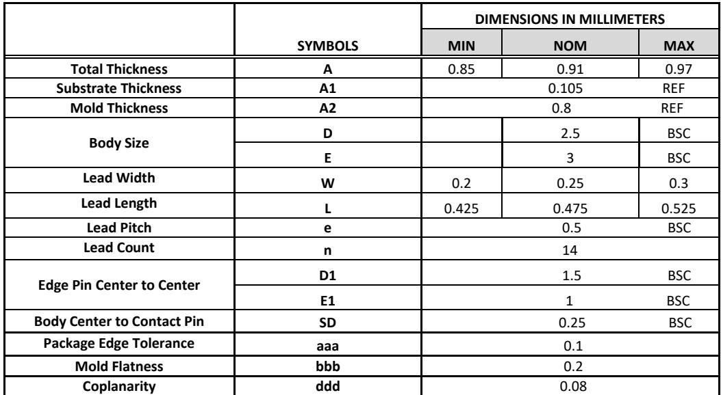
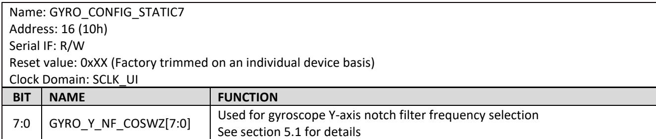
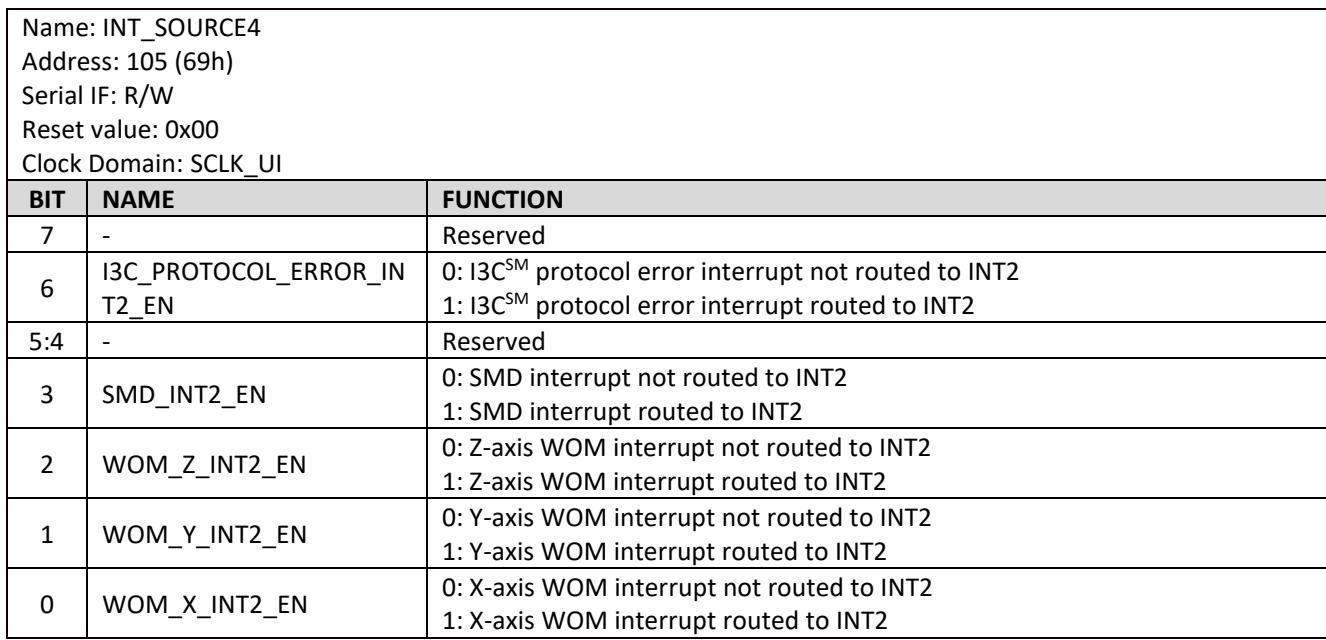
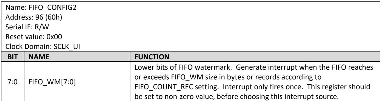
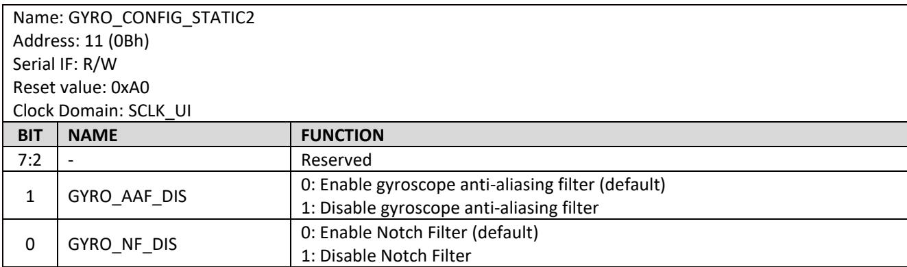
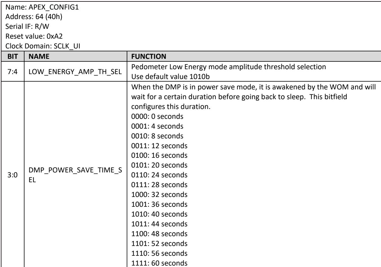

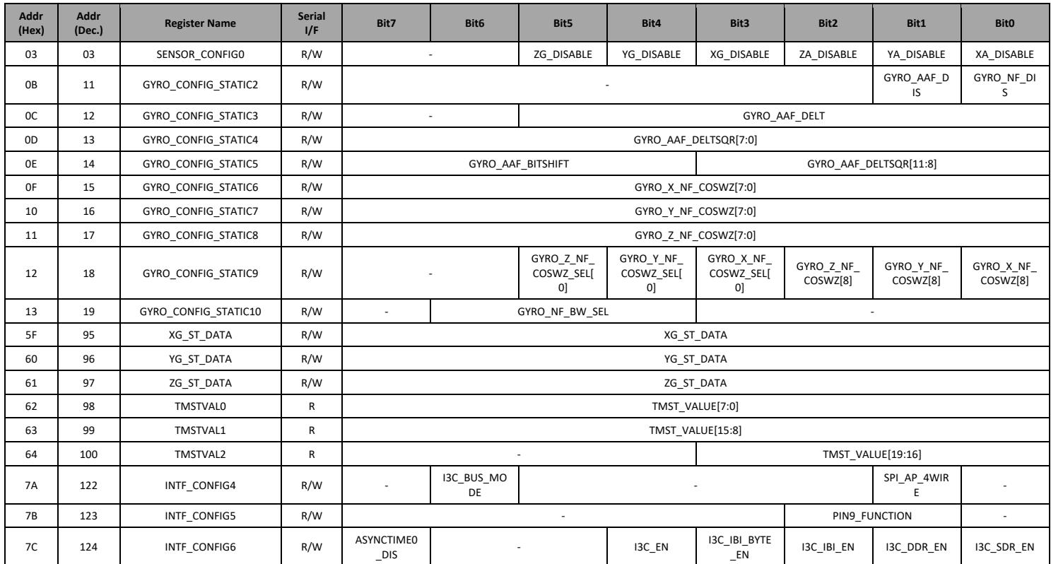
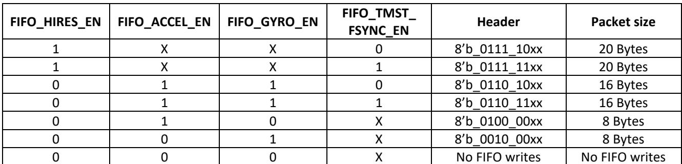
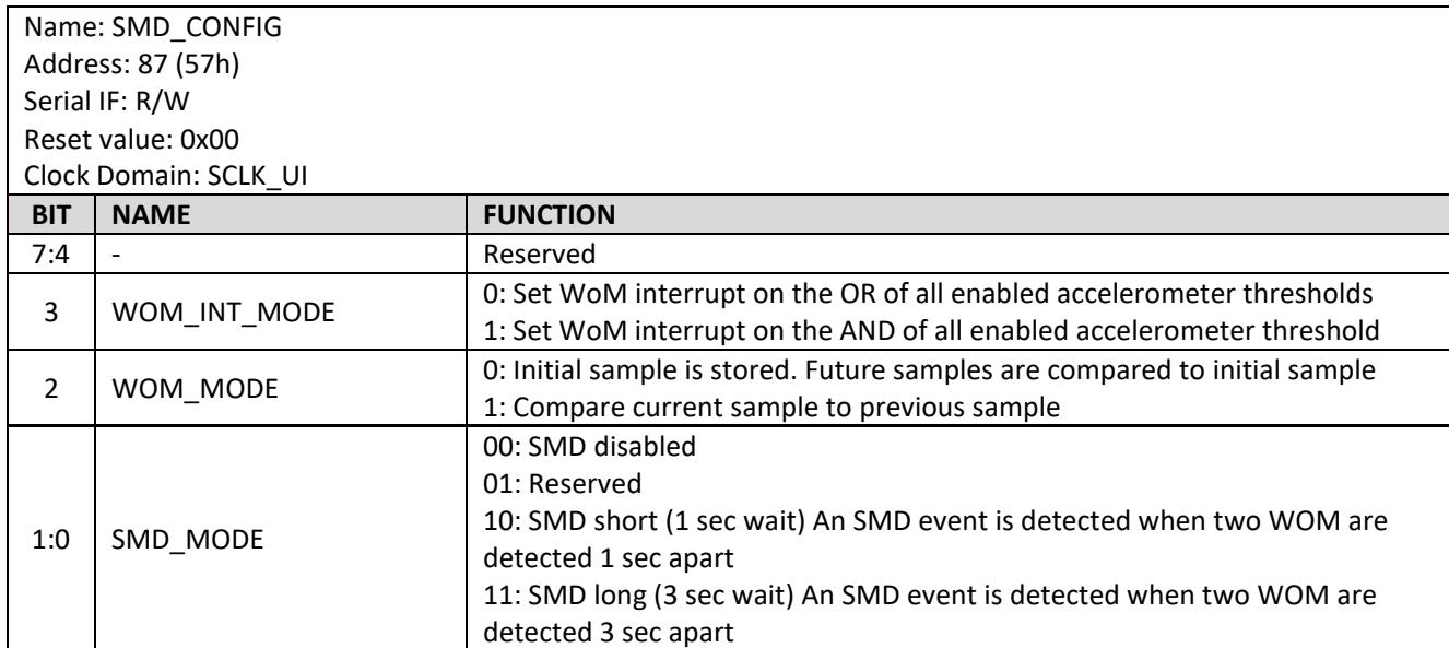
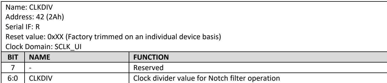
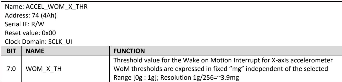


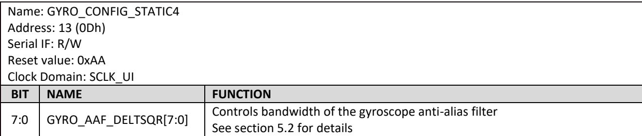

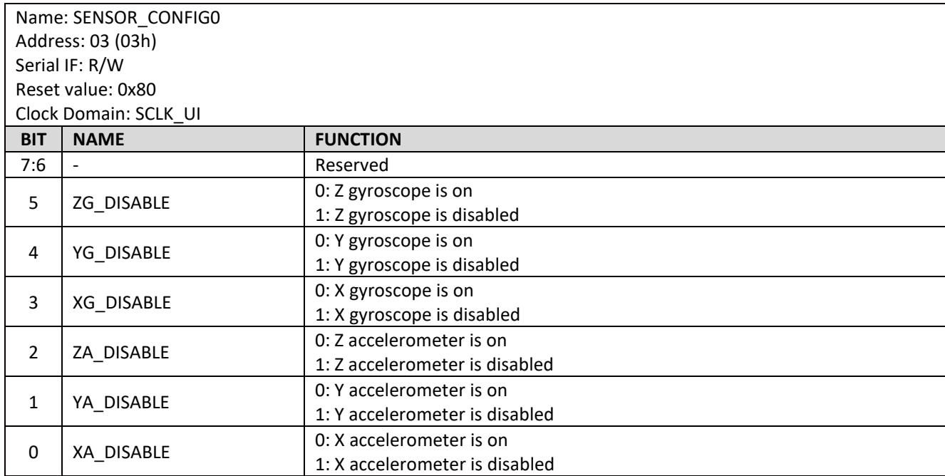


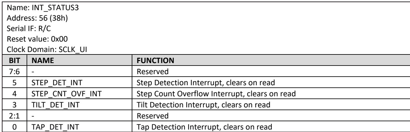
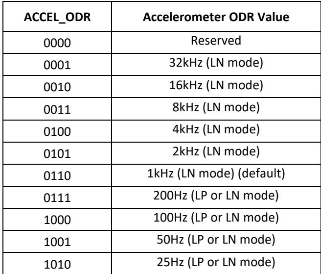
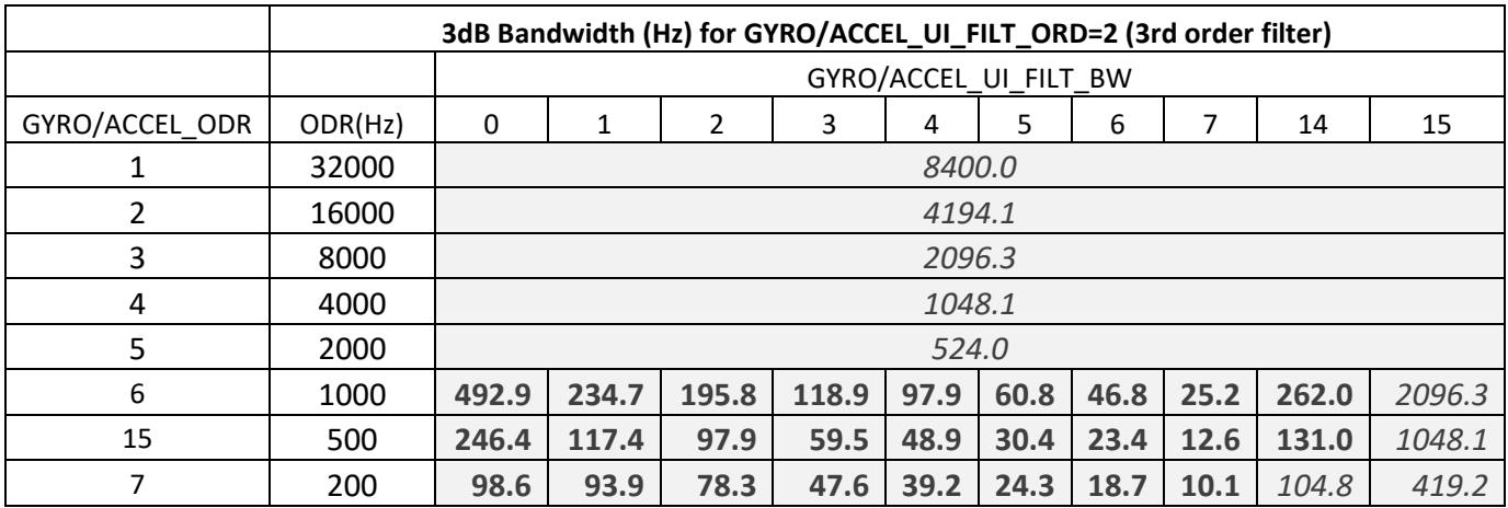
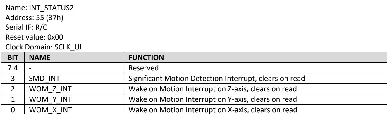
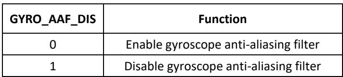
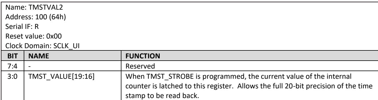
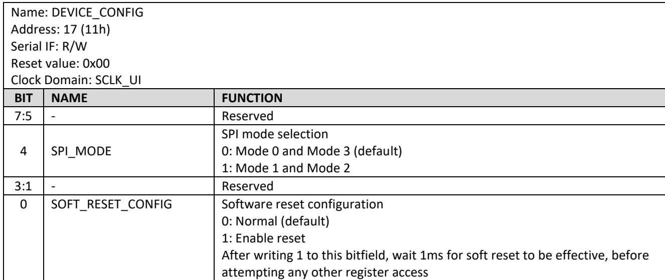
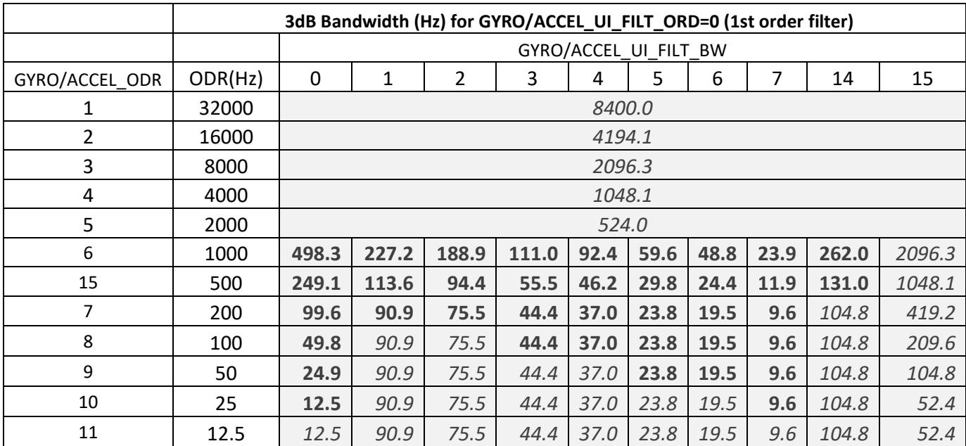
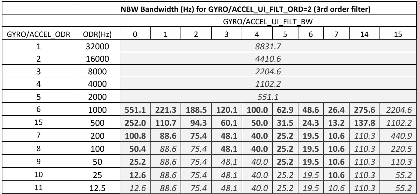
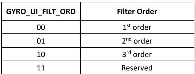
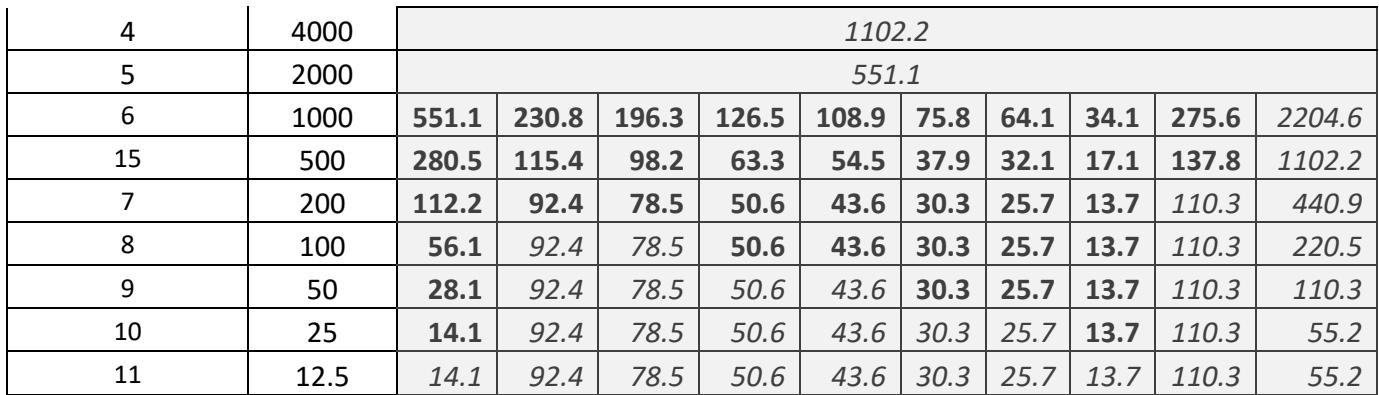
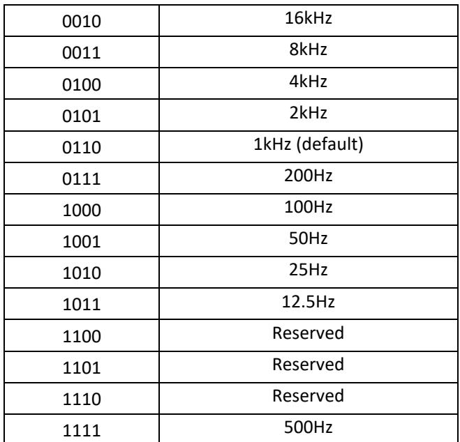
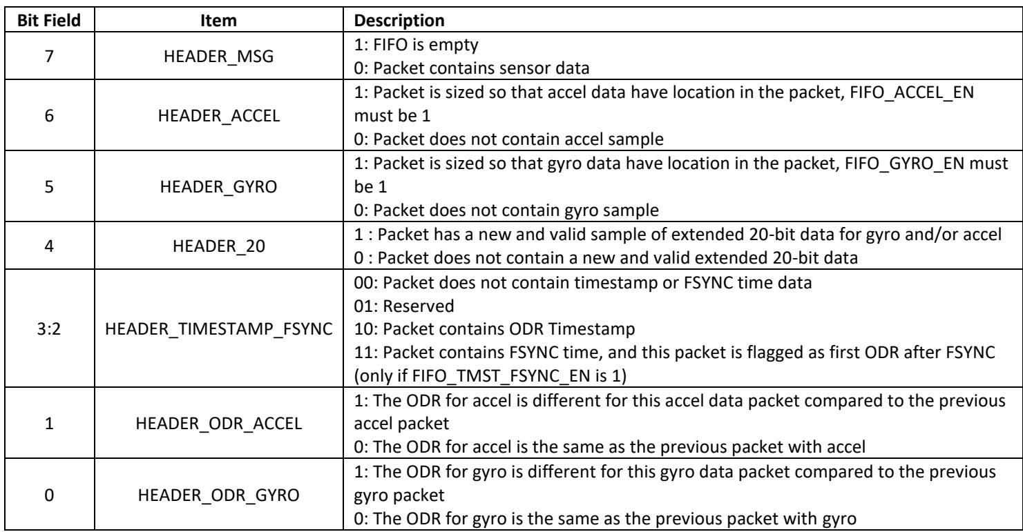
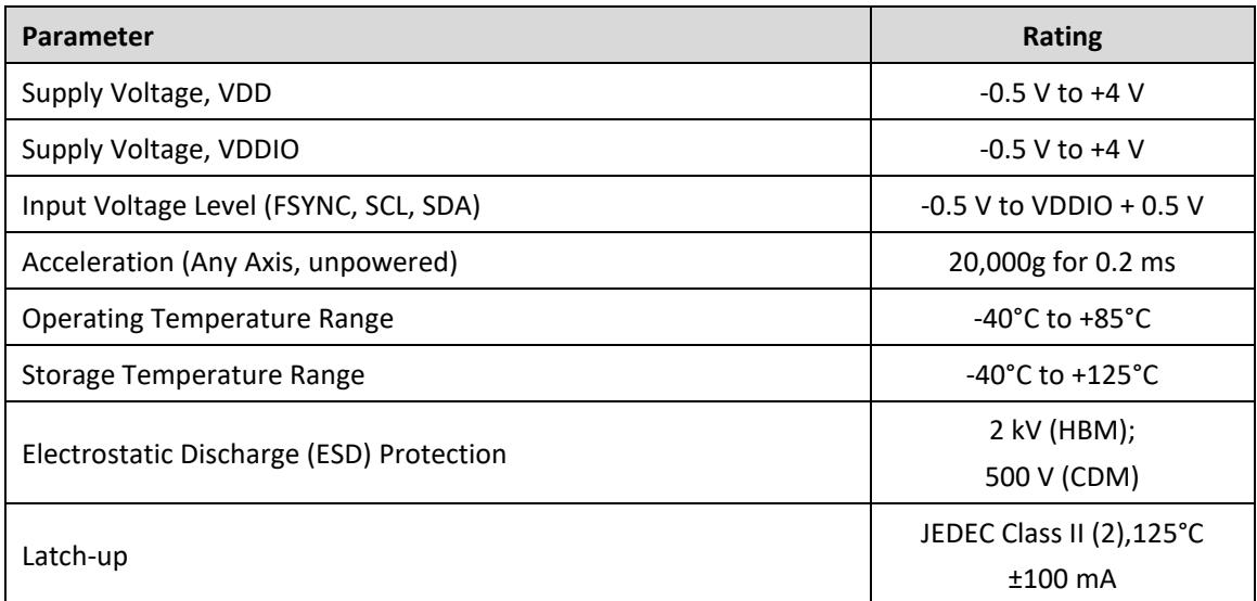

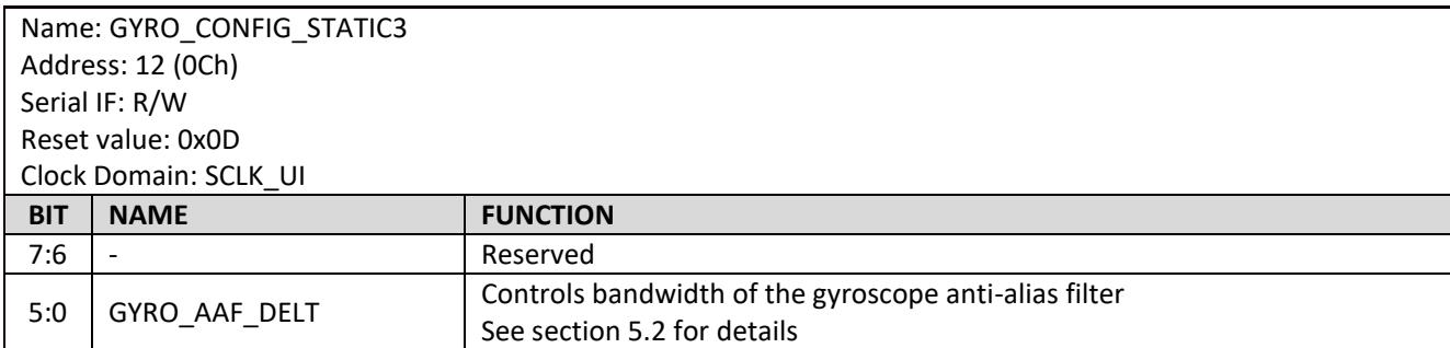
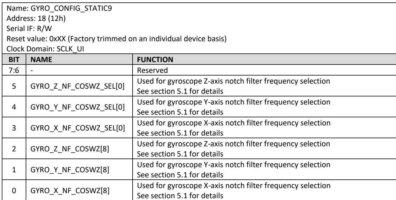

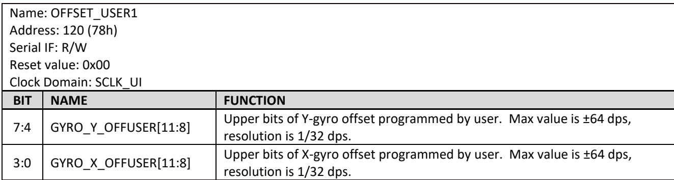

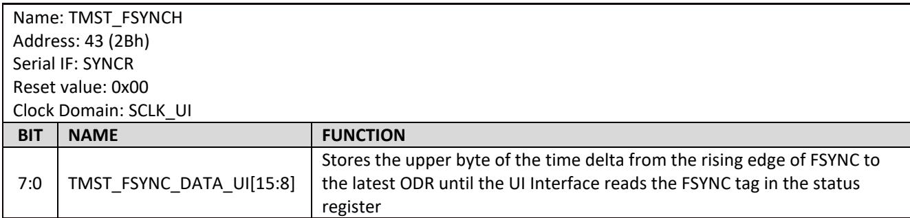
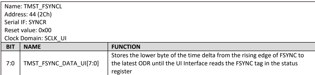
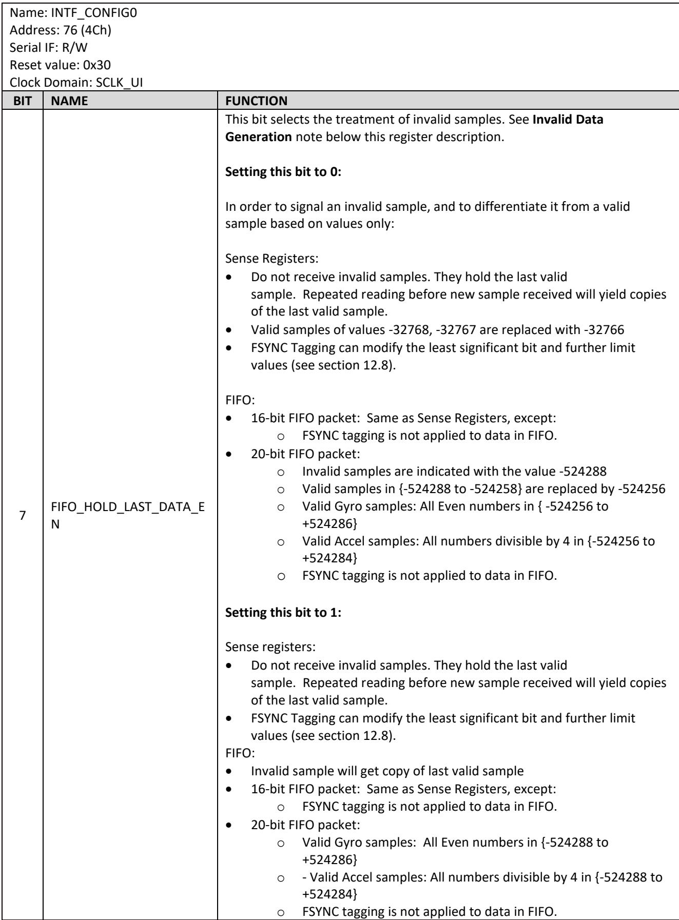
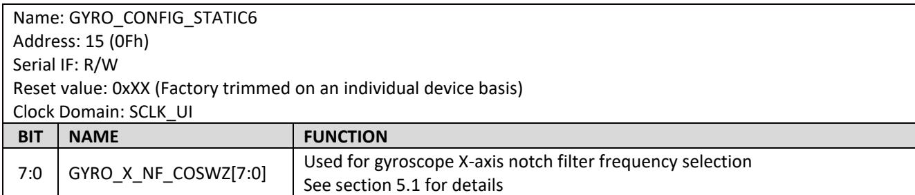

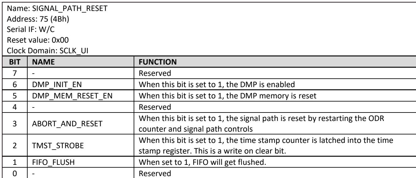
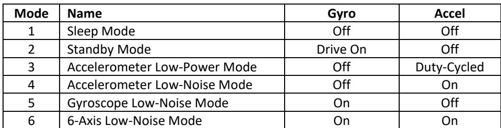

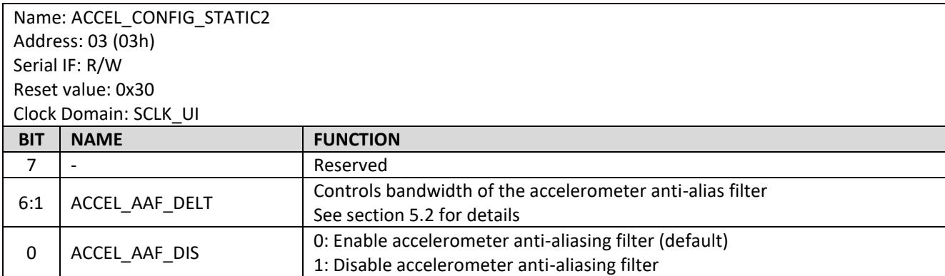
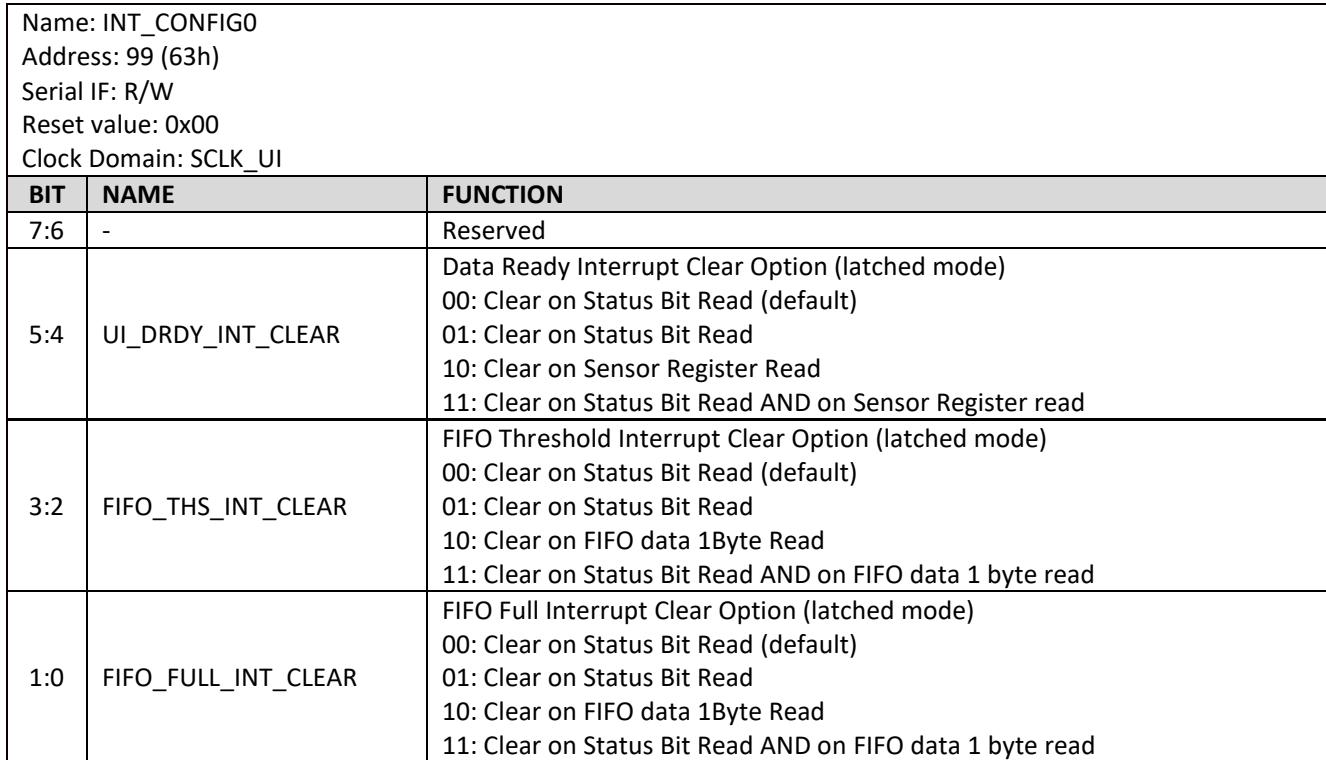


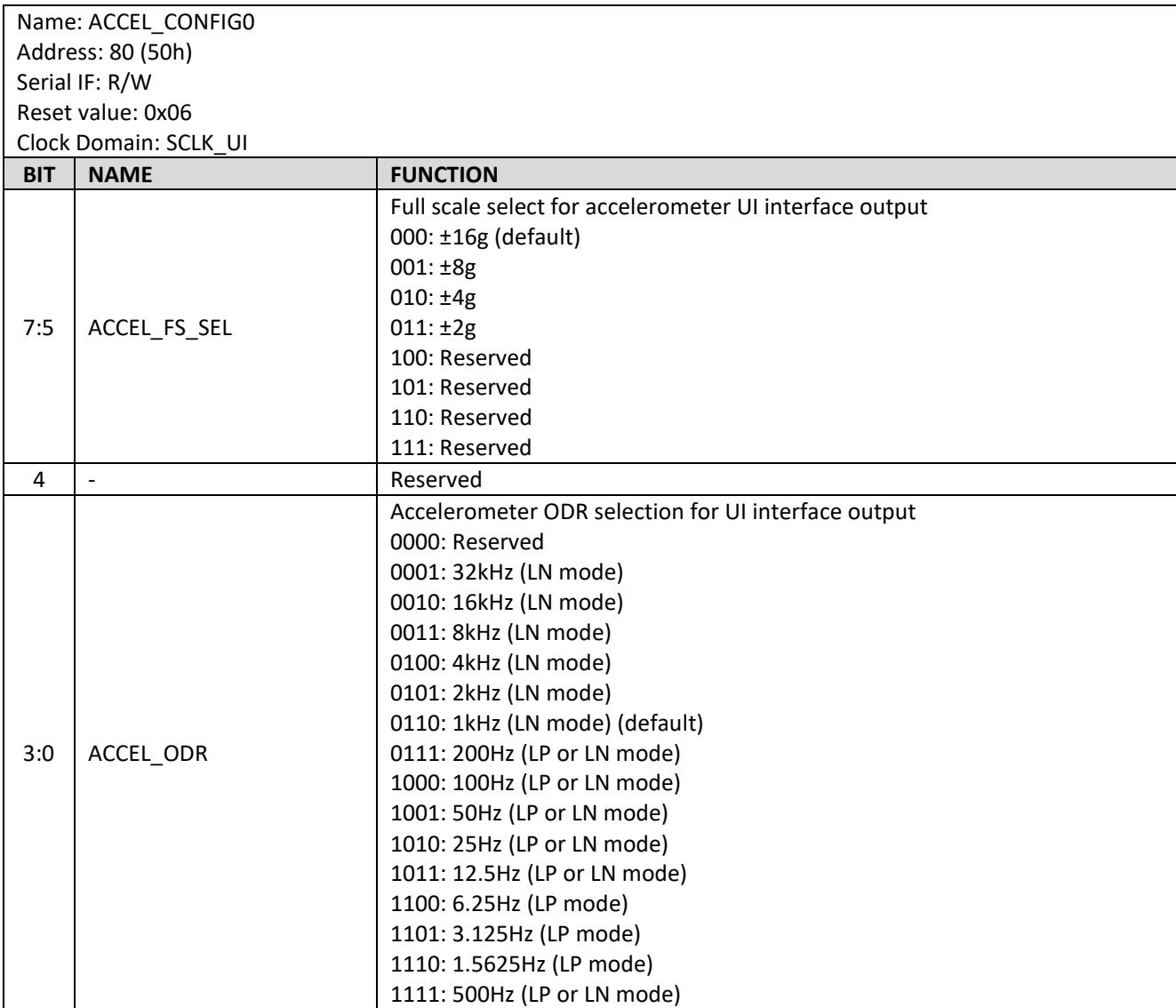

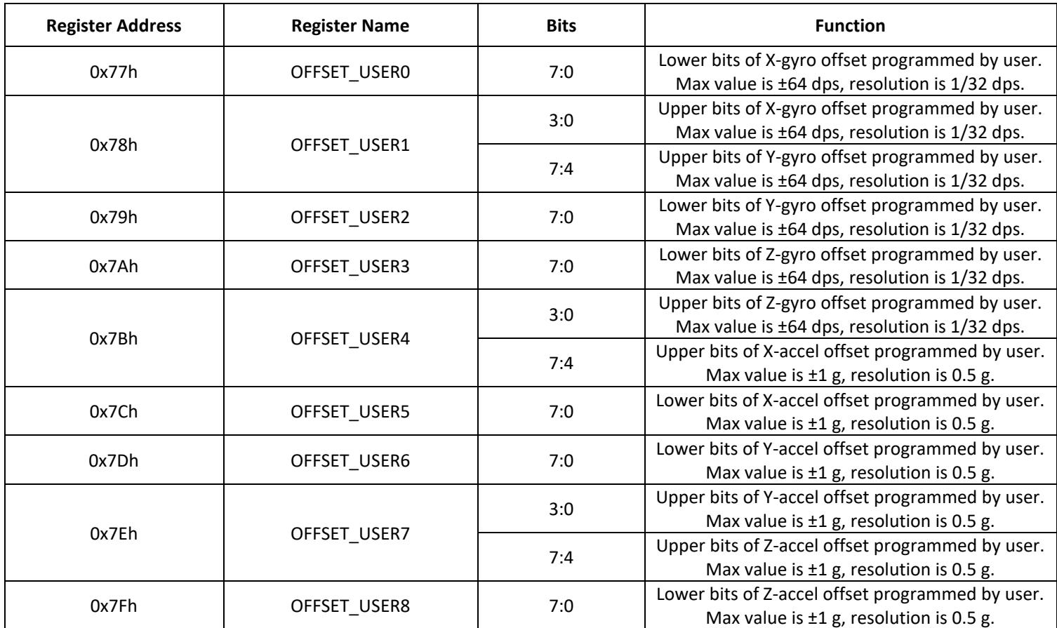
Use this datasheet from any agent
Send the page, markdown, chunks, or search endpoint to ChatGPT, Claude, embedr-app, or your own tooling.