
ADS7866
12-Bit, 200-kSPS, Micro-Power SAR ADC with SPI Interface
1 .2-V, 1 2-/1 0-/8-BIT, 200-KSPS/1 00-KSPS, M ICRO-POWER, M I N IATU RE ANALOG-TO-DIGITAL CONVERTER WITH SERIAL INTERFACE
FEATU RES
• Si ng le 1 .2-V to 3.6-V Su pply Operation
● H ig h Th roug h put – 200/240/280KSPS for 1 2/1 0/8-Bit $\mathsf { V } _ { \mathsf { D D } } \geq 1 . 6 \mathsf { V }$ – 1 00/1 20/1 40KSPS for 1 2/1 0/8-B it $\mathsf { V } _ { \mathsf { D D } } \geq 1 . 2 \mathsf { V }$
• ±1 .5LSB I N L 1 2-Bit N MC (ADS7866)
71 dB SN R –83 dB TH D at $\mathsf { f } _ { \mathsf { I N } } = 3 \mathsf { 0 }$ kHz (ADS7866)
• Synch ron ized Conversion with SCLK
• SPI Com pati ble Serial I nterface
• No Pi pel i ne Delays
• Low Power
– 1 .39 mW Typ at 200 KSPS $\mathsf { V } _ { \mathsf { D D } } = 3 . 6 \ \mathsf { V }$ – 0.39 mW Typ at 200 KSPS $\mathsf { V } _ { \mathsf { D D } } = 1 . 6 \mathsf { V }$ – 0.22 mW Typ at 1 00 KSPS $\mathsf { V } _ { \mathsf { D D } } = 1 . 2 \ : \mathsf { V }$
• Auto Power-Down : 8 nA Typ 300 nA Max
• 0 V to $\mathsf { v } _ { \mathsf { D } \mathsf { D } }$ U n i polar I n put Range
• 6-Pi n SOT-23 Package
APPLICATIONS
• Battery Powered Systems
• Isolated Data Acq u isition
• Med ical I nstru ments
• Portable Com m u n ication
• Portable Data Acq u isition Systems
• Automatic Test Eq u i pment
DESCRIPTION
The ADS7866/67/68 are low power m i n iatu re 1 2/1 0/8-bit A/D conve rte rs each with a u n i polar si ng le-ended i n put . These devices can ope rate from a si ng le 1 . 6 V to 3 . 6 V su pply with a 200- KS PS th rou g h p ut fo r ADS7866 . I n add ition these devi ces can mai ntai n at l east a 1 00- KS PS th rou g h p ut with a su pply as low as 1 2 V
The sam pl i ng conve rsion and activation of d ig ital output S DO are i n itiated on the fal l i ng edge of CS . The se rial clock SC LK is used fo r control l i ng the conve rsion rate and sh ifti ng data out of the conve rte r Fu rthermore SCLK provides a mechan ism to al low d i g ital host p rocesso rs to synch ron ize with the con - verter These conve rte rs i nte rface wit h m icro-p rocesso rs o r DS Ps th roug h a h ig h-speed S P I com pati ble se rial i nte rface . The re are no pi pel i ne delays associated with the device .
The m i n i m u m conve rsion ti me is dete rm i ned by the freq uency of the se rial clock i n put SC LK wh i le the maxi m u m freq uency of SC LK is dete rm i ned by the m i n i m u m sam pl i ng ti me req u i red to charge the i n p ut capacitance to 1 2/1 0/8-bit accu racy fo r the ADS7866/67/68 respectively. The maxi m u m th roug h put is dete rm i ned by how often a conve rsion is i n itiated when the m i n i m u m sam pl i ng ti me is met and the maxi m u m SC LK freq uency is used . E ach device automatical ly powe rs down afte r each conve rsion wh ich al lows each device to save powe r when the th rou g h p ut is red u ced wh i l e usi ng the maxi m u m SC LK freq uency.
The conve rte r refe rence is taken i nte rnal ly from the su pply. H ence the analog i n put range fo r these devices is 0 V to $\mathsf { V } _ { \mathsf { D D } }$
These devices are avai lable i n a 6-pi n SOT-23 package and are characte rized ove r the i nd ustrial –40°C to 85°C tem peratu re range .
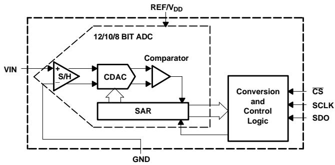
M icro-Power M i n iatu re SAR Converter Fam i ly
| RESOLUTION/SPEED | < 200 KSPS | 1 MSPS – 1.25 MSPS |
| 12-Bit | ADS7866 (1.2 VDD to 3.6 VDD) | ADS7886 (2.35 VDD to 5.25 VDD) |
| 10-Bit | ADS7867 (1.2 VDD to 3.6 VDD) | ADS7887 (2.35 VDD to 5.25 VDD) |
| 8-Bit | ADS7868 (1.2 VDD to 3.6 VDD) | ADS7888 (2.35 VDD to 5.25 VDD) |
P lease be aware that an i m po rtant notice conce rn i ng avai labi l ity standard warranty and use i n critical appl ications of Texas I nstru ments sem icond ucto r p rod ucts and d isclai me rs the reto appears at the end of th is data sheet .

These devices have l i m ited bu i lt-i n E S D p rotection The leads shou ld be shorted togethe r or the device placed i n cond uctive foam d u ri ng storage or hand l i ng to p revent electrostatic damage to the MOS gates .
ORDERING INFORMATION (1)
| MODEL | MAXIMUM INTEGRAL LINEARITY (LSB) | MAXIMUM DIFFERENTIAL LINEARITY (LSB) | NO MISSING CODES RESOLUTION (BIT) | PACKAGE TYPE | PACKAGE MARKING (SYMBOL) | PACKAGE DESIGNATOR | SPECIFIED TEMPERATURE RANGE | ORDERING NUMBER | TRANSPORT MEDIA, QUANTITY |
| ADS7866I | ±1.5 | -1/+1.5 | 12 | SOT23-6 | A66Y | DBV | -40°C to 85°C | ADS7866IDBVT | Small tape and reel, 250 |
| ADS7866I | ±1.5 | -1/+1.5 | 12 | SOT23-6 | A66Y | DBV | -40°C to 85°C | ADS7866IDBVR | Tape and reel, 3000 |
| ADS7867I | ±0.5 | ±0.5 | 10 | SOT23-6 | A67Y | DBV | -40°C to 85°C | ADS7867IDBVT | Small tape and reel, 250 |
| ADS7867I | ±0.5 | ±0.5 | 10 | SOT23-6 | A67Y | DBV | -40°C to 85°C | ADS7867IDBVR | Tape and reel, 3000 |
| ADS7868I | ±0.5 | ±0.5 | 8 | SOT23-6 | A68Y | DBV | -40°C to 85°C | ADS7868IDBVT | Small tape and reel, 250 |
| ADS7868I | ±0.5 | ±0.5 | 8 | SOT23-6 | A68Y | DBV | -40°C to 85°C | ADS7868IDBVR | Tape and reel, 3000 |
( 1 ) Fo r the most cu rrent package and o rde ri ng i nfo rmation , see the Package Option Addend u m at the end of th is docu ment , o r see the TI web site at www ti com
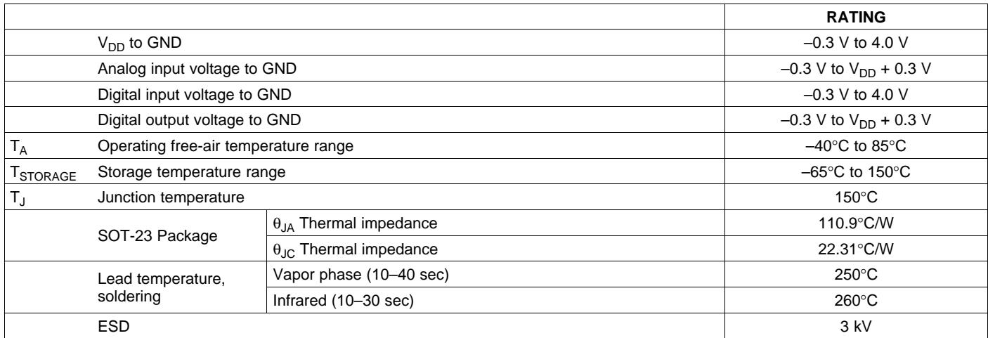
ABSOLUTE MAXIMUM RATINGS
ove r ope rati ng free-ai r tem pe ratu re range (u n less othe rwise noted)
| RATING | ||
| $V_{DD}$ to GND | -0.3 V to 4.0 V | |
| Analog input voltage to GND | -0.3 V to $V_{DD}$ + 0.3 V | |
| Digital input voltage to GND | -0.3 V to 4.0 V | |
| Digital output voltage to GND | -0.3 V to $V_{DD}$ + 0.3 V | |
| $T_A$ Operating free-air temperature range | -40°C to 85°C | |
| $T_{STORAGE}$ Storage temperature range | -65°C to 150°C | |
| $T_J$ Junction temperature | 150°C | |
| SOT-23 Package | $\theta_{JA}$ Thermal impedance | 110.9°C/W |
| $\theta_{JC}$ Thermal impedance | 22.31°C/W | |
| Lead temperature, soldering | Vapor phase (10–40 sec) | 250°C |
| Infrared (10–30 sec) | 260°C | |
| ESD | 3 kV | |
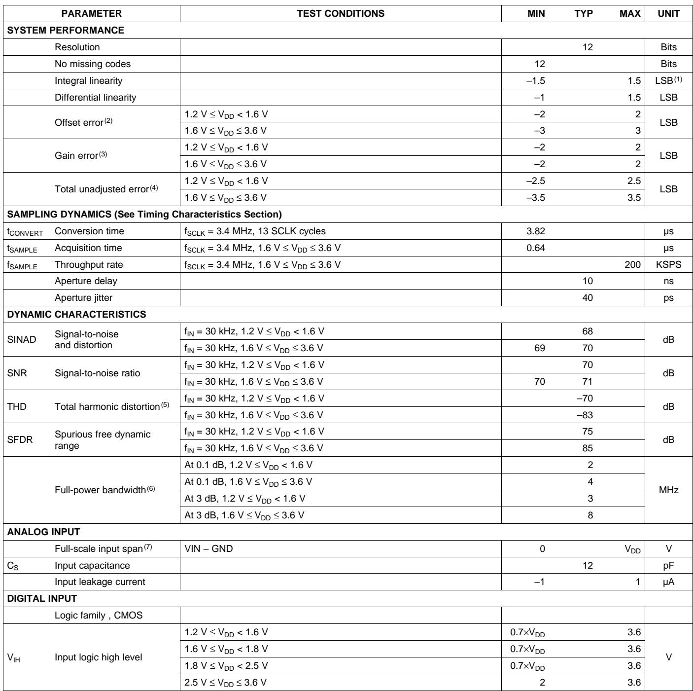
SPECI FICATIONS, ADS7866
$\mathsf { A t } - 4 0 ^ { \circ } \mathsf C$ to 85°C , $\mathsf { f } _ { \mathsf { S A M P L E } } = 2 0 0 \mathsf { K S P S }$ and $\mathsf { f } _ { \mathsf { S C L K } } = 3 . 4 \mathsf { M H z }$ i f 1 . $\mathrm { \ i \setminus } \le \mathsf { V } _ { \mathsf { D D } } \le 3 . 6 \lor ;$ $\mathsf { f } _ { \mathsf { S A M P L E } } = 1 0 0 \mathsf { K S P S }$ and $\mathsf { f } _ { \mathsf { S C L K } } = 1 . 7$ M Hz if $1 . 2 \vee \le \vee _ { \mathsf { D D } } < 1 . 6 \vee$ (u n less othe rwise noted)
| PARAMETER | TEST CONDITIONS | MIN | TYP | MAX | UNIT | |
| SYSTEM PERFORMANCE | ||||||
| Resolution | 12 | Bits | ||||
| No missing codes | 12 | Bits | ||||
| Integral linearity | -1.5 | 1.5 | LSB(1) | |||
| Differential linearity | -1 | 1.5 | LSB | |||
| Offset $error^{(2)}$ | $1.2\mathrm{V} \leq {\mathrm{V}}_{\mathrm{{DD}}} < {1.6}\mathrm{\;V}$ | -2 | 2 | LSB | ||
| $1.6\mathrm{V} \leq {\mathrm{V}}_{\mathrm{{DD}}} \leq {3.6}\mathrm{\;V}$ | -3 | 3 | ||||
| Gain $error^{(3)}$ | $1.2\mathrm{V} \leq {\mathrm{V}}_{\mathrm{{DD}}} < {1.6}\mathrm{\;V}$ | -2 | 2 | LSB | ||
| $1.6\mathrm{V} \leq {\mathrm{V}}_{\mathrm{{DD}}} \leq {3.6}\mathrm{\;V}$ | -2 | 2 | ||||
| Total unadjusted $error^{(4)}$ | $1.2\mathrm{V} \leq {\mathrm{V}}_{\mathrm{{DD}}} < {1.6}\mathrm{\;V}$ | -2.5 | 2.5 | LSB | ||
| $1.6\mathrm{V} \leq {\mathrm{V}}_{\mathrm{{DD}}} \leq {3.6}\mathrm{\;V}$ | -3.5 | 3.5 | ||||
| SAMPLING DYNAMICS (See Timing Characteristics Section) | ||||||
| $t_{CONVERT}$ | Conversion time | $f_{SCLK} = {3.4}\mathrm{{MHz}},{13}\mathrm{{SCLK}}$ cycles | 3.82 | μs | ||
| $t_{SAMPLE}$ | Acquisition time | $f_{SCLK} = {3.4}\mathrm{{MHz}},{1.6}\mathrm{\;V} \leq {\mathrm{V}}_{\mathrm{{DD}}} \leq {3.6}\mathrm{\;V}$ | 0.64 | μs | ||
| $f_{SAMPLE}$ | Throughput rate | $f_{SCLK} = {3.4}\mathrm{{MHz}},{1.6}\mathrm{\;V} \leq {\mathrm{V}}_{\mathrm{{DD}}} \leq {3.6}\mathrm{\;V}$ | 200 | KSPS | ||
| Aperture delay | 10 | ns | ||||
| Aperture jitter | 40 | ps | ||||
| DYNAMIC CHARACTERISTICS | ||||||
| SINAD | Signal-to-noise and distortion | $f_{IN} = {30}\mathrm{{kHz}},{1.2}\mathrm{\;V} \leq {\mathrm{V}}_{\mathrm{{DD}}} < {1.6}\mathrm{\;V}$ | 68 | dB | ||
| $f_{IN} = {30}\mathrm{{kHz}},{1.6}\mathrm{\;V} \leq {\mathrm{V}}_{\mathrm{{DD}}} \leq {3.6}\mathrm{\;V}$ | 69 | 70 | ||||
| SNR | Signal-to-noise ratio | $f_{IN} = {30}\mathrm{{kHz}},{1.2}\mathrm{\;V} \leq {\mathrm{V}}_{\mathrm{{DD}}} < {1.6}\mathrm{\;V}$ | 70 | dB | ||
| $f_{IN} = {30}\mathrm{{kHz}},{1.6}\mathrm{\;V} \leq {\mathrm{V}}_{\mathrm{{DD}}} \leq {3.6}\mathrm{\;V}$ | 70 | 71 | ||||
| THD | Total harmonic $distortion^{(5)}$ | $f_{IN} = {30}\mathrm{{kHz}},{1.2}\mathrm{\;V} \leq {\mathrm{V}}_{\mathrm{{DD}}} < {1.6}\mathrm{\;V}$ | -70 | dB | ||
| $f_{IN} = {30}\mathrm{{kHz}},{1.6}\mathrm{\;V} \leq {\mathrm{V}}_{\mathrm{{DD}}} \leq {3.6}\mathrm{\;V}$ | -83 | |||||
| SFDR | Spurious free dynamic range | $f_{IN} = {30}\mathrm{{kHz}},{1.2}\mathrm{\;V} \leq {\mathrm{V}}_{\mathrm{{DD}}} < {1.6}\mathrm{\;V}$ | 75 | dB | ||
| $f_{IN} = {30}\mathrm{{kHz}},{1.6}\mathrm{\;V} \leq {\mathrm{V}}_{\mathrm{{DD}}} \leq {3.6}\mathrm{\;V}$ | 85 | |||||
| Full-power $bandwidth^{(6)}$ | At 0.1 dB, ${1.2}\mathrm{\;V} \leq {\mathrm{V}}_{\mathrm{{DD}}} < {1.6}\mathrm{\;V}$ | 2 | MHz | |||
| At 0.1 dB, ${1.6}\mathrm{\;V} \leq {\mathrm{V}}_{\mathrm{{DD}}} \leq {3.6}\mathrm{\;V}$ | 4 | |||||
| At 3 dB, ${1.2}\mathrm{\;V} \leq {\mathrm{V}}_{\mathrm{{DD}}} < {1.6}\mathrm{\;V}$ | 3 | |||||
| At 3 dB, ${1.6}\mathrm{\;V} \leq {\mathrm{V}}_{\mathrm{{DD}}} \leq {3.6}\mathrm{\;V}$ | 8 | |||||
| ANALOG INPUT | ||||||
| Full-scale input $span^{(7)}$ | VIN - GND | 0 | $V_{DD}$ | V | ||
| $C_S$ | Input capacitance | 12 | pF | |||
| Input leakage current | -1 | 1 | μA | |||
| DIGITAL INPUT | ||||||
| Logic family , CMOS | ||||||
| $V_{IH}$ | Input logic high level | $1.2\mathrm{\;V} \leq {\mathrm{V}}_{\mathrm{{DD}}} < {1.6}\mathrm{\;V}$ | $0.7 \times {V}_{DD}$ | 3.6 | V | |
| $1.6\mathrm{\;V} \leq {\mathrm{V}}_{\mathrm{{DD}}} < {1.8}\mathrm{\;V}$ | $0.7 \times {V}_{DD}$ | 3.6 | ||||
| $1.8\mathrm{\;V} \leq {\mathrm{V}}_{\mathrm{{DD}}} < {2.5}\mathrm{\;V}$ | $0.7 \times {V}_{DD}$ | 3.6 | ||||
| $2.5\mathrm{\;V} \leq {\mathrm{V}}_{\mathrm{{DD}}} \leq {3.6}\mathrm{\;V}$ | 2 | 3.6 | ||||
( 1 ) L S B = Le ast S i g n i f i ca n t B I t
(2) The d iffe rence i n the fi rst code transition 000 . . . 000 to 000 . . . 00 1 from the ideal val u e of G N D + 1 LS B .
( 3 ) T h e d i ffe re n ce i n t h e l ast co d e t ra n s i t i o n 0 1 1 . . . 1 1 1 to 1 1 1 . . . 1 1 1 f ro m t h e i d e a l va l u e of $\mathsf { V } _ { \mathsf { D } \mathsf { D } } - 1$ LS B with the offset e rror removed
(4) The absol ute d iffe rence from the ideal transfe r fu nction of the conve rte r. Th is specifi cation is si m i lar to I N L e rro r except the effects of offset e rro r and gai n e rro r are i ncl uded .
(5) The 2 nd th roug h 1 0th harmon ics are used to dete rm i ne TH D .
(6) I n p ut freq u ency whe re the am pl itude of the d i g itized si g nal has decreased by 0 . 1 d B o r 3 d B .
(7) I deal i n p ut span wh i ch does not i ncl ude gai n o r offset e rro rs .
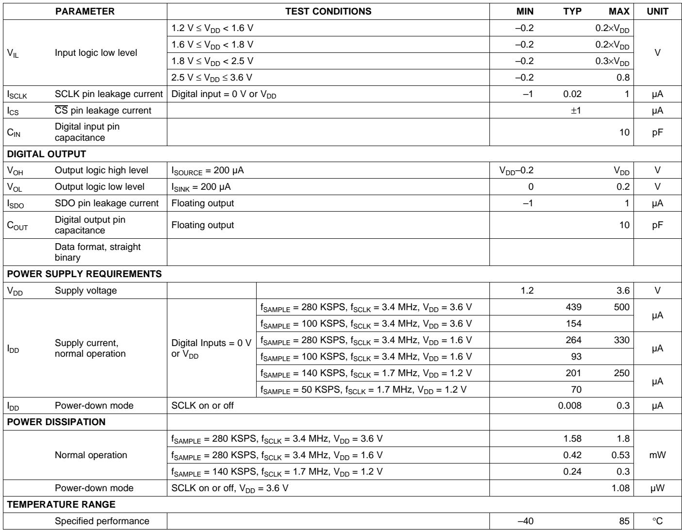
SPECI FICATIONS, ADS7866 (conti n ued)
At –40°C to 85°C $t _ { \mathsf { S A M P L E } } = 2 0 0$ KSPS and $\mathsf { f } _ { \mathsf { S C L K } } = 3 . 4$ M Hz if 1 6 $\mathsf { V } \leq \mathsf { V } _ { \mathsf { D D } } \leq 3 . 6 \mathsf { V } ;$ $\mathsf { f } _ { \mathsf { S A M P L E } } = 1 0 0 \mathsf { K S P S }$ and $\mathsf { f } _ { \mathsf { S C L K } } = 1 . 7$ M Hz if 1 . 2 $\mathsf { V } \leq \mathsf { V } _ { \mathsf { D D } } < 1 . 6 \mathsf { V }$ (u n l ess othe rwise noted)
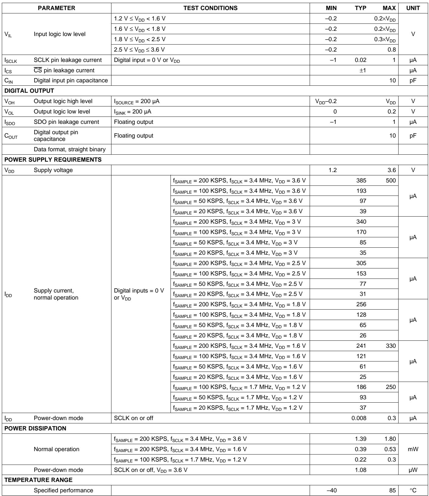
| PARAMETER | TEST CONDITIONS | MIN | TYP | MAX | UNIT | ||
| $V_{IL}$ | Input logic low level | 1.2 V ≤ $V_{DD}$ < 1.6 V | -0.2 | 0.2× $V_{DD}$ | V | ||
| 1.6 V ≤ $V_{DD}$ < 1.8 V | -0.2 | 0.2× $V_{DD}$ | |||||
| 1.8 V ≤ $V_{DD}$ < 2.5 V | -0.2 | 0.3× $V_{DD}$ | |||||
| 2.5 V ≤ $V_{DD}$ ≤ 3.6 V | -0.2 | 0.8 | |||||
| $I_{SCLK}$ | SCLK pin leakage current | Digital input = 0 V or $V_{DD}$ | -1 | 0.02 | 1 | μA | |
| $I_{CS}$ | $\overline{CS}$ pin leakage current | ±1 | μA | ||||
| $C_{IN}$ | Digital input pin capacitance | 10 | pF | ||||
| DIGITAL OUTPUT | |||||||
| $V_{OH}$ | Output logic high level | $I_{SOURCE}$ = 200 μA | $V_{DD}$ -0.2 | $V_{DD}$ | V | ||
| $V_{OL}$ | Output logic low level | $I_{SINK}$ = 200 μA | 0 | 0.2 | V | ||
| $I_{SDO}$ | SDO pin leakage current | Floating output | -1 | 1 | μA | ||
| $C_{OUT}$ | Digital output pin capacitance | Floating output | 10 | pF | |||
| Data format, straight binary | |||||||
| POWER SUPPLY REQUIREMENTS | |||||||
| $V_{DD}$ | Supply voltage | 1.2 | 3.6 | V | |||
| $I_{DD}$ | Supply current, normal operation | Digital inputs = 0 V or $V_{DD}$ | $f_{SAMPLE}$ = 200 KSPS, $f_{SCLK}$ = 3.4 MHz, $V_{DD}$ = 3.6 V | 385 | 500 | μA | |
| $f_{SAMPLE}$ = 100 KSPS, $f_{SCLK}$ = 3.4 MHz, $V_{DD}$ = 3.6 V | 193 | ||||||
| $f_{SAMPLE}$ = 50 KSPS, $f_{SCLK}$ = 3.4 MHz, $V_{DD}$ = 3.6 V | 97 | ||||||
| $f_{SAMPLE}$ = 20 KSPS, $f_{SCLK}$ = 3.4 MHz, $V_{DD}$ = 3.6 V | 39 | ||||||
| $f_{SAMPLE}$ = 200 KSPS, $f_{SCLK}$ = 3.4 MHz, $V_{DD}$ = 3 V | 340 | μA | |||||
| $f_{SAMPLE}$ = 100 KSPS, $f_{SCLK}$ = 3.4 MHz, $V_{DD}$ = 3 V | 170 | ||||||
| $f_{SAMPLE}$ = 50 KSPS, $f_{SCLK}$ = 3.4 MHz, $V_{DD}$ = 3 V | 85 | ||||||
| $f_{SAMPLE}$ = 20 KSPS, $f_{SCLK}$ = 3.4 MHz, $V_{DD}$ = 3 V | 35 | ||||||
| $f_{SAMPLE}$ = 200 KSPS, $f_{SCLK}$ = 3.4 MHz, $V_{DD}$ = 2.5 V | 305 | μA | |||||
| $f_{SAMPLE}$ = 100 KSPS, $f_{SCLK}$ = 3.4 MHz, $V_{DD}$ = 2.5 V | 153 | ||||||
| $f_{SAMPLE}$ = 50 KSPS, $f_{SCLK}$ = 3.4 MHz, $V_{DD}$ = 2.5 V | 77 | ||||||
| $f_{SAMPLE}$ = 20 KSPS, $f_{SCLK}$ = 3.4 MHz, $V_{DD}$ = 2.5 V | 31 | ||||||
| $f_{SAMPLE}$ = 200 KSPS, $f_{SCLK}$ = 3.4 MHz, $V_{DD}$ = 1.8 V | 256 | μA | |||||
| $f_{SAMPLE}$ = 100 KSPS, $f_{SCLK}$ = 3.4 MHz, $V_{DD}$ = 1.8 V | 128 | ||||||
| $f_{SAMPLE}$ = 50 KSPS, $f_{SCLK}$ = 3.4 MHz, $V_{DD}$ = 1.8 V | 65 | ||||||
| $f_{SAMPLE}$ = 20 KSPS, $f_{SCLK}$ = 3.4 MHz, $V_{DD}$ = 1.8 V | 26 | ||||||
| $f_{SAMPLE}$ = 200 KSPS, $f_{SCLK}$ = 3.4 MHz, $V_{DD}$ = 1.6 V | 241 | 330 | μA | ||||
| $f_{SAMPLE}$ = 100 KSPS, $f_{SCLK}$ = 3.4 MHz, $V_{DD}$ = 1.6 V | 121 | ||||||
| $f_{SAMPLE}$ = 50 KSPS, $f_{SCLK}$ = 3.4 MHz, $V_{DD}$ = 1.6 V | 61 | ||||||
| $f_{SAMPLE}$ = 20 KSPS, $f_{SCLK}$ = 3.4 MHz, $V_{DD}$ = 1.6 V | 25 | ||||||
| $f_{SAMPLE}$ = 100 KSPS, $f_{SCLK}$ = 1.7 MHz, $V_{DD}$ = 1.2 V | 186 | 250 | μA | ||||
| $f_{SAMPLE}$ = 50 KSPS, $f_{SCLK}$ = 1.7 MHz, $V_{DD}$ = 1.2 V | 93 | ||||||
| $f_{SAMPLE}$ = 20 KSPS, $f_{SCLK}$ = 1.7 MHz, $V_{DD}$ = 1.2 V | 37 | ||||||
| $I_{DD}$ | Power-down mode | SCLK on or off | 0.008 | 0.3 | μA | ||
| POWER DISSIPATION | |||||||
| Normal operation | $f_{SAMPLE}$ = 200 KSPS, $f_{SCLK}$ = 3.4 MHz, $V_{DD}$ = 3.6 V | 1.39 | 1.80 | mW | |||
| $f_{SAMPLE}$ = 200 KSPS, $f_{SCLK}$ = 3.4 MHz, $V_{DD}$ = 1.6 V | 0.39 | 0.53 | |||||
| $f_{SAMPLE}$ = 100 KSPS, $f_{SCLK}$ = 1.7 MHz, $V_{DD}$ = 1.2 V | 0.22 | 0.3 | |||||
| Power-down mode | SCLK on or off, $V_{DD}$ = 3.6 V | 1.08 | μW | ||||
| TEMPERATURE RANGE | |||||||
| Specified performance | -40 | 85 | °C | ||||
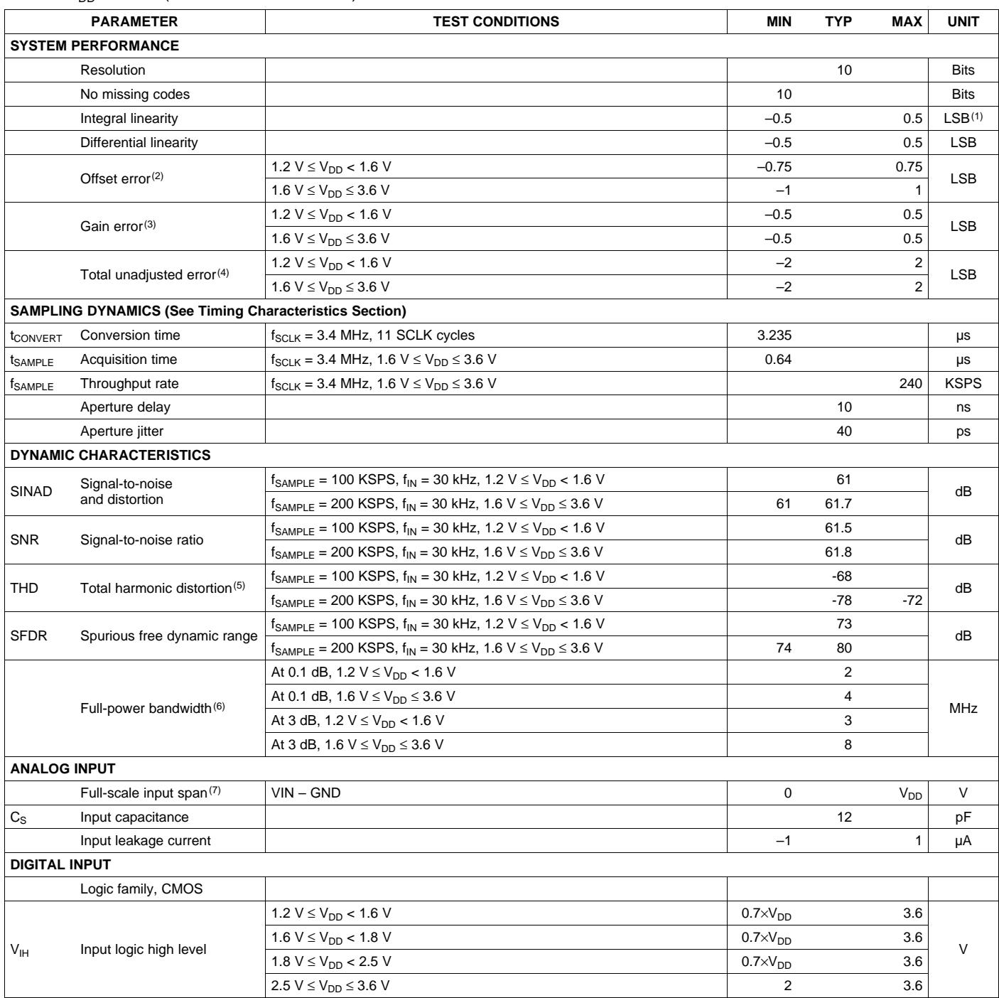
SPECI FICATIONS, ADS7867
$\mathsf { A t } - 4 0 ^ { \circ } \mathsf C$ to 85°C , $\mathsf { f } _ { \mathsf { S A M P L E } } = 2 4 0 \mathsf { K S P S }$ and $\mathsf { f } _ { \mathsf { S C L K } } = 3 . 4$ M H z if 1 $6 \mathsf { V } \leq \mathsf { V } _ { \mathsf { D D } } \leq 3 . 6 \mathsf { V } ;$ $\mathsf { f } _ { \mathsf { S A M P L E } } = 1 2 0$ KSPS and $\mathsf { f } _ { \mathsf { S C L K } } = 1 . 7$ M Hz if $1 . 2 \vee \le \vee _ { \mathsf { D D } } < 1 . 6 \vee$ (u n less othe rwise noted)
| PARAMETER | TEST CONDITIONS | MIN | TYP | MAX | UNIT | |
| SYSTEM PERFORMANCE | ||||||
| Resolution | 10 | Bits | ||||
| No missing codes | 10 | Bits | ||||
| Integral linearity | -0.5 | 0.5 | LSB(1) | |||
| Differential linearity | -0.5 | 0.5 | LSB | |||
| Offset $error^{(2)}$ | $1.2\mathrm{V} \leq {\mathrm{V}}_{\mathrm{{DD}}} < {1.6}\mathrm{\;V}$ | -0.75 | 0.75 | LSB | ||
| $1.6\mathrm{V} \leq {\mathrm{V}}_{\mathrm{{DD}}} \leq {3.6}\mathrm{\;V}$ | -1 | 1 | ||||
| Gain $error^{(3)}$ | $1.2\mathrm{V} \leq {\mathrm{V}}_{\mathrm{{DD}}} < {1.6}\mathrm{\;V}$ | -0.5 | 0.5 | LSB | ||
| $1.6\mathrm{V} \leq {\mathrm{V}}_{\mathrm{{DD}}} \leq {3.6}\mathrm{\;V}$ | -0.5 | 0.5 | ||||
| Total unadjusted $error^{(4)}$ | $1.2\mathrm{V} \leq {\mathrm{V}}_{\mathrm{{DD}}} < {1.6}\mathrm{\;V}$ | -2 | 2 | LSB | ||
| $1.6\mathrm{V} \leq {\mathrm{V}}_{\mathrm{{DD}}} \leq {3.6}\mathrm{\;V}$ | -2 | 2 | ||||
| SAMPLING DYNAMICS (See Timing Characteristics Section) | ||||||
| $t_{CONVERT}$ | Conversion time | $f_{SCLK} = {3.4}\mathrm{{MHz}},{11}\mathrm{{SCLK}}$ cycles | 3.235 | μs | ||
| $t_{SAMPLE}$ | Acquisition time | $f_{SCLK} = {3.4}\mathrm{{MHz}},{1.6}\mathrm{\;V} \leq {\mathrm{V}}_{\mathrm{{DD}}} \leq {3.6}\mathrm{\;V}$ | 0.64 | μs | ||
| $f_{SAMPLE}$ | Throughput rate | $f_{SCLK} = {3.4}\mathrm{{MHz}},{1.6}\mathrm{\;V} \leq {\mathrm{V}}_{\mathrm{{DD}}} \leq {3.6}\mathrm{\;V}$ | 240 | KSPS | ||
| Aperture delay | 10 | ns | ||||
| Aperture jitter | 40 | ps | ||||
| DYNAMIC CHARACTERISTICS | ||||||
| SINAD | Signal-to-noise and distortion | $f_{SAMPLE} = {100}\mathrm{{KSPS}},{f}_{IN} = {30}\mathrm{{kHz}},{1.2}\mathrm{\;V} \leq {\mathrm{V}}_{\mathrm{{DD}}} < {1.6}\mathrm{\;V}$ | 61 | dB | ||
| $f_{SAMPLE} = {200}\mathrm{{KSPS}},{f}_{IN} = {30}\mathrm{{kHz}},{1.6}\mathrm{\;V} \leq {\mathrm{V}}_{\mathrm{{DD}}} \leq {3.6}\mathrm{\;V}$ | 61 | 61.7 | ||||
| SNR | Signal-to-noise ratio | $f_{SAMPLE} = {100}\mathrm{{KSPS}},{f}_{IN} = {30}\mathrm{{kHz}},{1.2}\mathrm{\;V} \leq {\mathrm{V}}_{\mathrm{{DD}}} < {1.6}\mathrm{\;V}$ | 61.5 | dB | ||
| $f_{SAMPLE} = {200}\mathrm{{KSPS}},{f}_{IN} = {30}\mathrm{{kHz}},{1.6}\mathrm{\;V} \leq {\mathrm{V}}_{\mathrm{{DD}}} \leq {3.6}\mathrm{\;V}$ | 61.8 | |||||
| THD | Total harmonic $distortion^{(5)}$ | $f_{SAMPLE} = {100}\mathrm{{KSPS}},{f}_{IN} = {30}\mathrm{{kHz}},{1.2}\mathrm{\;V} \leq {\mathrm{V}}_{\mathrm{{DD}}} < {1.6}\mathrm{\;V}$ | -68 | dB | ||
| $f_{SAMPLE} = {200}\mathrm{{KSPS}},{f}_{IN} = {30}\mathrm{{kHz}},{1.6}\mathrm{\;V} \leq {\mathrm{V}}_{\mathrm{{DD}}} \leq {3.6}\mathrm{\;V}$ | -78 | -72 | ||||
| SFDR | Spurious free dynamic range | $f_{SAMPLE} = {100}\mathrm{{KSPS}},{f}_{IN} = {30}\mathrm{{kHz}},{1.2}\mathrm{\;V} \leq {\mathrm{V}}_{\mathrm{{DD}}} < {1.6}\mathrm{\;V}$ | 73 | dB | ||
| $f_{SAMPLE} = {200}\mathrm{{KSPS}},{f}_{IN} = {30}\mathrm{{kHz}},{1.6}\mathrm{\;V} \leq {\mathrm{V}}_{\mathrm{{DD}}} \leq {3.6}\mathrm{\;V}$ | 74 | 80 | ||||
| Full-power $bandwidth^{(6)}$ | At 0.1 dB, ${1.2}\mathrm{\;V} \leq {\mathrm{V}}_{\mathrm{{DD}}} < {1.6}\mathrm{\;V}$ | 2 | MHz | |||
| At 0.1 dB, ${1.6}\mathrm{\;V} \leq {\mathrm{V}}_{\mathrm{{DD}}} \leq {3.6}\mathrm{\;V}$ | 4 | |||||
| At 3 dB, ${1.2}\mathrm{\;V} \leq {\mathrm{V}}_{\mathrm{{DD}}} < {1.6}\mathrm{\;V}$ | 3 | |||||
| At 3 dB, ${1.6}\mathrm{\;V} \leq {\mathrm{V}}_{\mathrm{{DD}}} \leq {3.6}\mathrm{\;V}$ | 8 | |||||
| ANALOG INPUT | ||||||
| Full-scale input $span^{(7)}$ | VIN - GND | 0 | $V_{DD}$ | V | ||
| $C_S$ | Input capacitance | 12 | pF | |||
| Input leakage current | -1 | 1 | μA | |||
| DIGITAL INPUT | ||||||
| Logic family, CMOS | ||||||
| $V_{IH}$ | Input logic high level | $1.2\mathrm{\;V} \leq {\mathrm{V}}_{\mathrm{{DD}}} < {1.6}\mathrm{\;V}$ | $0.7 \times {V}_{DD}$ | 3.6 | V | |
| $1.6\mathrm{\;V} \leq {\mathrm{V}}_{\mathrm{{DD}}} < {1.8}\mathrm{\;V}$ | $0.7 \times {V}_{DD}$ | 3.6 | ||||
| $1.8\mathrm{\;V} \leq {\mathrm{V}}_{\mathrm{{DD}}} < {2.5}\mathrm{\;V}$ | $0.7 \times {V}_{DD}$ | 3.6 | ||||
| $2.5\mathrm{\;V} \leq {\mathrm{V}}_{\mathrm{{DD}}} \leq {3.6}\mathrm{\;V}$ | 2 | 3.6 | ||||
( 1 ) L S B = Le ast S i g n i f i ca n t B I t
(2) The d iffe rence i n the fi rst code transition 000 . . . 000 to 000 . . . 00 1 from the ideal val u e of G N D + 1 LS B .
( 3 ) T h e d i ffe re n ce i n t h e l ast co d e t ra n s i t i o n 0 1 1 . . . 1 1 1 to 1 1 1 . . . 1 1 1 f ro m t h e i d e a l va l u e of $\mathsf { V } _ { \mathsf { D } \mathsf { D } } - 1$ LS B with the offset e rror removed
(4) The absol ute d iffe rence from the ideal transfe r fu nction of the conve rte r. Th is specifi cation is si m i lar to I N L e rro r except the effects of offset e rro r and gai n e rro r are i ncl uded .
(5) The 2 nd th roug h 1 0th harmon ics are used to dete rm i ne TH D .
(6) I n p ut freq u ency whe re the am pl itude of the d i g itized si g nal has decreased by 0 . 1 d B o r 3 d B .
(7) I deal i n p ut span wh i ch does not i ncl ude gai n o r offset e rro rs .
SPECI FICATIONS, ADS7867 (conti n ued)
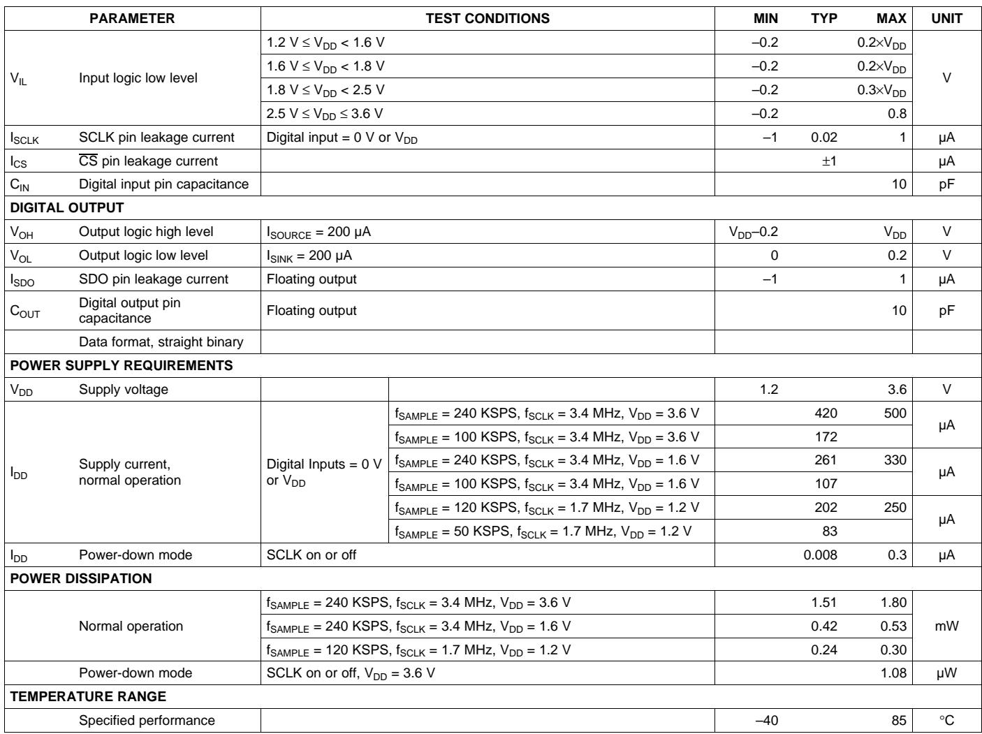
At –40°C to 85°C $\mathsf { f } _ { \mathsf { S A M P L E } } = 2 4 0$ KSPS and $\mathsf { f } _ { \mathsf { S C L K } } = 3 . 4$ M Hz if 1 6 $\mathsf { V } \leq \mathsf { V } _ { \mathsf { D D } } \leq 3 . 6 \mathsf { V } ;$ $\mathsf { f } _ { \mathsf { S A M P L E } } = 1 2 0 \mathsf { K S P S }$ and $\mathsf { f } _ { \mathsf { S C L K } } = 1 . 7$ M Hz if 1 . 2 $\mathsf { V } \leq \mathsf { V } _ { \mathsf { D D } } < 1 . 6 \mathsf { V }$ (u n less othe rwise noted)
| PARAMETER | TEST CONDITIONS | MIN | TYP | MAX | UNIT | ||
| $V_{IL}$ | Input logic low level | 1.2 V ≤ $V_{DD}$ < 1.6 V | -0.2 | 0.2× $V_{DD}$ | V | ||
| 1.6 V ≤ $V_{DD}$ < 1.8 V | -0.2 | 0.2× $V_{DD}$ | |||||
| 1.8 V ≤ $V_{DD}$ < 2.5 V | -0.2 | 0.3× $V_{DD}$ | |||||
| 2.5 V ≤ $V_{DD}$ ≤ 3.6 V | -0.2 | 0.8 | |||||
| $I_{SCLK}$ | SCLK pin leakage current | Digital input = 0 V or $V_{DD}$ | -1 | 0.02 | 1 | μA | |
| $I_{CS}$ | $\overline{CS}$ pin leakage current | ±1 | μA | ||||
| $C_{IN}$ | Digital input pin capacitance | 10 | pF | ||||
| DIGITAL OUTPUT | |||||||
| $V_{OH}$ | Output logic high level | $I_{SOURCE}$ = 200 μA | $V_{DD}$ -0.2 | $V_{DD}$ | V | ||
| $V_{OL}$ | Output logic low level | $I_{SINK}$ = 200 μA | 0 | 0.2 | V | ||
| $I_{SDO}$ | SDO pin leakage current | Floating output | -1 | 1 | μA | ||
| $C_{OUT}$ | Digital output pin capacitance | Floating output | 10 | pF | |||
| Data format, straight binary | |||||||
| POWER SUPPLY REQUIREMENTS | |||||||
| $V_{DD}$ | Supply voltage | 1.2 | 3.6 | V | |||
| $I_{DD}$ | Supply current, normal operation | Digital Inputs = 0 V or $V_{DD}$ | $f_{SAMPLE}$ = 240 KSPS, $f_{SCLK}$ = 3.4 MHz, $V_{DD}$ = 3.6 V | 420 | 500 | μA | |
| $f_{SAMPLE}$ = 100 KSPS, $f_{SCLK}$ = 3.4 MHz, $V_{DD}$ = 3.6 V | 172 | ||||||
| $f_{SAMPLE}$ = 240 KSPS, $f_{SCLK}$ = 3.4 MHz, $V_{DD}$ = 1.6 V | 261 | 330 | μA | ||||
| $f_{SAMPLE}$ = 100 KSPS, $f_{SCLK}$ = 3.4 MHz, $V_{DD}$ = 1.6 V | 107 | ||||||
| $f_{SAMPLE}$ = 120 KSPS, $f_{SCLK}$ = 1.7 MHz, $V_{DD}$ = 1.2 V | 202 | 250 | μA | ||||
| $f_{SAMPLE}$ = 50 KSPS, $f_{SCLK}$ = 1.7 MHz, $V_{DD}$ = 1.2 V | 83 | ||||||
| $I_{DD}$ | Power-down mode | SCLK on or off | 0.008 | 0.3 | μA | ||
| POWER DISSIPATION | |||||||
| Normal operation | $f_{SAMPLE}$ = 240 KSPS, $f_{SCLK}$ = 3.4 MHz, $V_{DD}$ = 3.6 V | 1.51 | 1.80 | mW | |||
| $f_{SAMPLE}$ = 240 KSPS, $f_{SCLK}$ = 3.4 MHz, $V_{DD}$ = 1.6 V | 0.42 | 0.53 | |||||
| $f_{SAMPLE}$ = 120 KSPS, $f_{SCLK}$ = 1.7 MHz, $V_{DD}$ = 1.2 V | 0.24 | 0.30 | |||||
| Power-down mode | SCLK on or off, $V_{DD}$ = 3.6 V | 1.08 | μW | ||||
| TEMPERATURE RANGE | |||||||
| Specified performance | -40 | 85 | °C | ||||
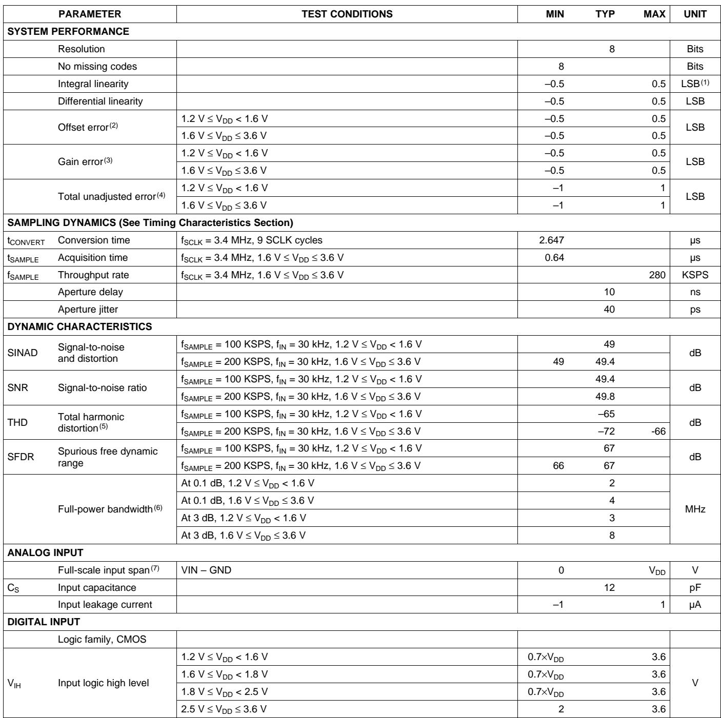
SPECI FICATIONS, ADS7868
$\mathsf { A t } - 4 0 ^ { \circ } \mathsf C$ to $8 5 ^ { \circ } \mathsf { C } , \mathsf { f } _ { \mathsf { S A M P L E } } = 2 8 0 \mathsf { K S P S }$ and $\mathsf { f } _ { \mathsf { S C L K } } = 3 . 4 \mathsf { M H z }$ i f 1 . $\mathfrak { I } \vee \le \vee _ { \mathsf { D D } } \le 3 . 6 \vee ; \mathfrak { f } _ { \mathsf { S A M P L E } } = 1 4 0 \mathsf { K S P S }$ and $\mathsf { f } _ { \mathsf { S C L K } } = 1 . 7$ M Hz if $1 . 2 \vee \le \vee _ { \mathsf { D D } } < 1 . 6 \vee$ (u n less othe rwise noted)
| PARAMETER | TEST CONDITIONS | MIN | TYP | MAX | UNIT | |
| SYSTEM PERFORMANCE | ||||||
| Resolution | 8 | Bits | ||||
| No missing codes | 8 | Bits | ||||
| Integral linearity | -0.5 | 0.5 | $LSB^{(1)}$ | |||
| Differential linearity | -0.5 | 0.5 | LSB | |||
| $Offset\ error^{(2)}$ | 1.2 V ≤ $V_{DD}$ < 1.6 V | -0.5 | 0.5 | LSB | ||
| 1.6 V ≤ $V_{DD}$ ≤ 3.6 V | -0.5 | 0.5 | ||||
| $Gain\ error^{(3)}$ | 1.2 V ≤ $V_{DD}$ < 1.6 V | -0.5 | 0.5 | LSB | ||
| 1.6 V ≤ $V_{DD}$ ≤ 3.6 V | -0.5 | 0.5 | ||||
| Total unadjusted $error^{(4)}$ | 1.2 V ≤ $V_{DD}$ < 1.6 V | -1 | 1 | LSB | ||
| 1.6 V ≤ $V_{DD}$ ≤ 3.6 V | -1 | 1 | ||||
| SAMPLING DYNAMICS (See Timing Characteristics Section) | ||||||
| $t_{CONVERT}$ | Conversion time | $f_{SCLK}$ = 3.4 MHz, 9 SCLK cycles | 2.647 | μs | ||
| $t_{SAMPLE}$ | Acquisition time | $f_{SCLK}$ = 3.4 MHz, 1.6 V ≤ $V_{DD}$ ≤ 3.6 V | 0.64 | μs | ||
| $f_{SAMPLE}$ | Throughput rate | $f_{SCLK}$ = 3.4 MHz, 1.6 V ≤ $V_{DD}$ ≤ 3.6 V | 280 | KSPS | ||
| Aperture delay | 10 | ns | ||||
| Aperture jitter | 40 | ps | ||||
| DYNAMIC CHARACTERISTICS | ||||||
| SINAD | Signal-to-noise and distortion | $f_{SAMPLE}$ = 100 KSPS, $f_{IN}$ = 30 kHz, 1.2 V ≤ $V_{DD}$ < 1.6 V | 49 | dB | ||
| $f_{SAMPLE}$ = 200 KSPS, $f_{IN}$ = 30 kHz, 1.6 V ≤ $V_{DD}$ ≤ 3.6 V | 49 | 49.4 | ||||
| SNR | Signal-to-noise ratio | $f_{SAMPLE}$ = 100 KSPS, $f_{IN}$ = 30 kHz, 1.2 V ≤ $V_{DD}$ < 1.6 V | 49.4 | dB | ||
| $f_{SAMPLE}$ = 200 KSPS, $f_{IN}$ = 30 kHz, 1.6 V ≤ $V_{DD}$ ≤ 3.6 V | 49.8 | |||||
| THD | Total harmonic distortion(5) | $f_{SAMPLE}$ = 100 KSPS, $f_{IN}$ = 30 kHz, 1.2 V ≤ $V_{DD}$ < 1.6 V | -65 | dB | ||
| $f_{SAMPLE}$ = 200 KSPS, $f_{IN}$ = 30 kHz, 1.6 V ≤ $V_{DD}$ ≤ 3.6 V | -72 | -66 | ||||
| SFDR | Spurious free dynamic range | $f_{SAMPLE}$ = 100 KSPS, $f_{IN}$ = 30 kHz, 1.2 V ≤ $V_{DD}$ < 1.6 V | 67 | dB | ||
| $f_{SAMPLE}$ = 200 KSPS, $f_{IN}$ = 30 kHz, 1.6 V ≤ $V_{DD}$ ≤ 3.6 V | 66 | 67 | ||||
| Full-power bandwidth(6) | At 0.1 dB, 1.2 V ≤ $V_{DD}$ < 1.6 V | 2 | MHz | |||
| At 0.1 dB, 1.6 V ≤ $V_{DD}$ ≤ 3.6 V | 4 | |||||
| At 3 dB, 1.2 V ≤ $V_{DD}$ < 1.6 V | 3 | |||||
| At 3 dB, 1.6 V ≤ $V_{DD}$ ≤ 3.6 V | 8 | |||||
| ANALOG INPUT | ||||||
| Full-scale input span(7) | VIN - GND | 0 | $V_{DD}$ | V | ||
| $C_S$ | Input capacitance | 12 | pF | |||
| Input leakage current | -1 | 1 | μA | |||
| DIGITAL INPUT | ||||||
| Logic family, CMOS | ||||||
| $V_{IH}$ | Input logic high level | 1.2 V ≤ $V_{DD}$ < 1.6 V | 0.7× $V_{DD}$ | 3.6 | V | |
| 1.6 V ≤ $V_{DD}$ < 1.8 V | 0.7× $V_{DD}$ | 3.6 | ||||
| 1.8 V ≤ $V_{DD}$ < 2.5 V | 0.7× $V_{DD}$ | 3.6 | ||||
| 2.5 V ≤ $V_{DD}$ ≤ 3.6 V | 2 | 3.6 | ||||
( 1 ) L S B = Le ast S i g n i f i ca n t B I t
(2) The d iffe rence i n the fi rst code transition 000 . . . 000 to 000 . . . 00 1 from the ideal val u e of G N D + 1 LS B .
( 3 ) T h e d i ffe re n ce i n t h e l ast co d e t ra n s i t i o n 0 1 1 . . . 1 1 1 to 1 1 1 . . . 1 1 1 f ro m t h e i d e a l va l u e of $\mathsf { V } _ { \mathsf { D } \mathsf { D } } - 1$ LS B with the offset e rror removed
(4) The absol ute d iffe rence from the ideal transfe r fu nction of the conve rte r. Th is specifi cation is si m i lar to I N L e rro r except the effects of offset e rro r and gai n e rro r are i ncl uded .
(5) The 2 nd th roug h 1 0th harmon ics are used to dete rm i ne TH D .
(6) I n p ut freq u ency whe re the am pl itude of the d i g itized si g nal has decreased by 0 . 1 d B o r 3 d B .
(7) I deal i n p ut span wh i ch does not i ncl ude gai n o r offset e rro rs .
SPECI FICATIONS, ADS7868 (conti n ued)
At –40°C to 85°C $\mathsf { f } _ { \mathsf { S A M P L E } } = 2 8 0$ KSPS and $\mathsf { f } _ { \mathsf { S C L K } } = 3 . 4 \mathsf { M H z }$ i f 1 . 6 $\mathsf { V } \leq \mathsf { V } _ { \mathsf { D D } } \leq 3 . 6 \mathsf { V } ;$ $\mathsf { f } _ { \mathsf { S A M P L E } } = 1 4 0 \mathsf { K S P S }$ and $\mathsf { f } _ { \mathsf { S C L K } } = 1 . 7$ M Hz if $1 . 2 \vee \le \vee _ { \mathsf { D D } } < 1 . 6 \vee$ (u n less othe rwise noted)
| PARAMETER | TEST CONDITIONS | MIN | TYP | MAX | UNIT | ||
| $V_{IL}$ | Input logic low level | 1.2 V ≤ $V_{DD}$ < 1.6 V | -0.2 | 0.2× $V_{DD}$ | V | ||
| 1.6 V ≤ $V_{DD}$ < 1.8 V | -0.2 | 0.2× $V_{DD}$ | |||||
| 1.8 V ≤ $V_{DD}$ < 2.5 V | -0.2 | 0.3× $V_{DD}$ | |||||
| 2.5 V ≤ $V_{DD}$ ≤ 3.6 V | -0.2 | 0.8 | |||||
| $I_{SCLK}$ | SCLK pin leakage current | Digital input = 0 V or $V_{DD}$ | -1 | 0.02 | 1 | μA | |
| $I_{CS}$ | $\overline{CS}$ pin leakage current | ±1 | μA | ||||
| $C_{IN}$ | Digital input pin capacitance | 10 | pF | ||||
| DIGITAL OUTPUT | |||||||
| $V_{OH}$ | Output logic high level | $I_{SOURCE}$ = 200 μA | $V_{DD}$ -0.2 | $V_{DD}$ | V | ||
| $V_{OL}$ | Output logic low level | $I_{SINK}$ = 200 μA | 0 | 0.2 | V | ||
| $I_{SDO}$ | SDO pin leakage current | Floating output | -1 | 1 | μA | ||
| $C_{OUT}$ | Digital output pin capacitance | Floating output | 10 | pF | |||
| Data format, straight binary | |||||||
| POWER SUPPLY REQUIREMENTS | |||||||
| $V_{DD}$ | Supply voltage | 1.2 | 3.6 | V | |||
| $I_{DD}$ | Supply current, normal operation | Digital Inputs = 0 V or $V_{DD}$ | $f_{SAMPLE}$ = 280 KSPS, $f_{SCLK}$ = 3.4 MHz, $V_{DD}$ = 3.6 V | 439 | 500 | μA | |
| $f_{SAMPLE}$ = 100 KSPS, $f_{SCLK}$ = 3.4 MHz, $V_{DD}$ = 3.6 V | 154 | ||||||
| $f_{SAMPLE}$ = 280 KSPS, $f_{SCLK}$ = 3.4 MHz, $V_{DD}$ = 1.6 V | 264 | 330 | μA | ||||
| $f_{SAMPLE}$ = 100 KSPS, $f_{SCLK}$ = 3.4 MHz, $V_{DD}$ = 1.6 V | 93 | ||||||
| $f_{SAMPLE}$ = 140 KSPS, $f_{SCLK}$ = 1.7 MHz, $V_{DD}$ = 1.2 V | 201 | 250 | μA | ||||
| $f_{SAMPLE}$ = 50 KSPS, $f_{SCLK}$ = 1.7 MHz, $V_{DD}$ = 1.2 V | 70 | ||||||
| $I_{DD}$ | Power-down mode | SCLK on or off | 0.008 | 0.3 | μA | ||
| POWER DISSIPATION | |||||||
| Normal operation | $f_{SAMPLE}$ = 280 KSPS, $f_{SCLK}$ = 3.4 MHz, $V_{DD}$ = 3.6 V | 1.58 | 1.8 | mW | |||
| $f_{SAMPLE}$ = 280 KSPS, $f_{SCLK}$ = 3.4 MHz, $V_{DD}$ = 1.6 V | 0.42 | 0.53 | |||||
| $f_{SAMPLE}$ = 140 KSPS, $f_{SCLK}$ = 1.7 MHz, $V_{DD}$ = 1.2 V | 0.24 | 0.3 | |||||
| Power-down mode | SCLK on or off, $V_{DD}$ = 3.6 V | 1.08 | μW | ||||
| TEMPERATURE RANGE | |||||||
| Specified performance | -40 | 85 | °C | ||||
TIMING REQUIREMENTS( )( )
$\mathsf { A t } - 4 0 ^ { \circ } \mathsf C$ to 85°C $\mathsf { f } _ { \mathsf { S C L K } } = 3 . 4 \mathsf { M H z }$ i f 1 . 6 $\mathsf { V } \leq \mathsf { V } _ { \mathsf { D D } } \leq 3 . 6 \mathsf { V } ; \mathsf { f } _ { \mathsf { S C L K } } = 1 . 7$ M Hz if $1 . 2 \mathrm { V } \leq \mathrm { V } _ { \mathsf { D D } } < 1 . 6 \mathrm { V } ,$ 50-p F Load on S DO Pi n u n less othe rwise noted
| PARAMETER | TEST CONDITIONS | MIN | TYP | MAX | UNIT | |
| $t_{sample}$ | Sample time | $t_{SU(CSF-FSCLKF)} + 2 \times t_{C(SCLK)}$ | μs | |||
| $t_{convert}$ | Conversion time | ADS7866 | 13 × $t_{C(SCLK)}$ | μs | ||
| ADS7867 | 11 × $t_{C(SCLK)}$ | |||||
| ADS7868 | 9 × $t_{C(SCLK)}$ | |||||
| $t_{C(SCLK)}$ | Cycle time | 1.2 V ≤ $V_{DD}$ < 1.6 V | See (3) | 100 | μs | |
| 1.6 V ≤ $V_{DD}$ < 1.8 V | See (3) | 100 | ||||
| 1.8 V ≤ $V_{DD}$ < 2.5 V | See (3) | 50 | ||||
| 2.5 V ≤ $V_{DD}$ ≤ 3.6 V | See (3) | 6.7 | ||||
| $t_{WH(SCLK)}$ | Pulse duration | 0.4 × $t_{C(SCLK)}$ | 0.6 × $t_{C(SCLK)}$ | ns | ||
| $t_{WL(SCLK)}$ | Pulse duration | 0.4 × $t_{C(SCLK)}$ | 0.6 × $t_{C(SCLK)}$ | ns | ||
| $t_{SU(CSF-FSCLKF)}$ | Setup time | 1.2 V ≤ $V_{DD}$ < 1.6 V | 192 | ns | ||
| 1.6 V ≤ $V_{DD}$ < 1.8 V | 55 | |||||
| 1.8 V ≤ $V_{DD}$ ≤ 3.6 V | 55 | |||||
| $t_{D(CSF-SDOVALID)}$ | Delay time | 1.2 V ≤ $V_{DD}$ < 1.6 V | 65 | ns | ||
| 1.6 V ≤ $V_{DD}$ < 1.8 V | 55 | |||||
| 1.8 V ≤ $V_{DD}$ ≤ 3.6 V | 55 | |||||
| $t_{H(SCLKF-SDOVALID)}$ | Hold time | 1.2 V ≤ $V_{DD}$ < 1.6 V | 20 | ns | ||
| 1.6 V ≤ $V_{DD}$ < 1.8 V | 10 | |||||
| 1.8 V ≤ $V_{DD}$ ≤ 3.6 V | 10 | |||||
| $t_{D(SCLKF-SDOVALID)}$ | Delay time | 1.2 V ≤ $V_{DD}$ < 1.6 V | 140 | ns | ||
| 1.6 V ≤ $V_{DD}$ < 1.8 V | 140 | |||||
| 1.8 V ≤ $V_{DD}$ ≤ 3.6 V | 140 | |||||
| $t_{DIS(EOC-SDOZ)}$ | Disable time | 1.2 V ≤ $V_{DD}$ < 1.6 V | 10 | 80 | ns | |
| 1.6 V ≤ $V_{DD}$ < 1.8 V | 7 | 60 | ||||
| 1.8 V ≤ $V_{DD}$ ≤ 3.6 V | 7 | 60 | ||||
| $t_{WH(CS)}$ | Pulse duration | 1.2 V ≤ $V_{DD}$ < 1.6 V | 20 | ns | ||
| 1.6 V ≤ $V_{DD}$ < 1.8 V | 10 | |||||
| 1.8 V ≤ $V_{DD}$ ≤ 3.6 V | 10 | |||||
| $t_{SU(LSBZ-CSF)}$ | Setup time | 1.2 V ≤ $V_{DD}$ < 1.6 V | 20 | ns | ||
| 1.6 V ≤ $V_{DD}$ < 1.8 V | 10 | |||||
| 1.8 V ≤ $V_{DD}$ ≤ 3.6 V | 10 | |||||
( 1 ) A l l i n p u t s i g n a l s a re s p e c i f i e d w i t h $\mathfrak { t } _ { \mathtt { f } } = \mathfrak { t } _ { \mathtt { f } } = 5$ ns ( 1 0% to 90% of $\mathsf { V } _ { \mathsf { D D } } )$ and ti med from a voltage level of $( \mathsf { V } _ { \mathsf { I L } } + \mathsf { V } _ { \mathsf { I H } } ) / 2 .$
(2 ) S e e t i m i n g d i a g ra m i n F i g u re 1 .
( 3 ) M i n $\mathsf { t } _ { \mathsf { C } ( \mathsf { S C L K } ) }$ is dete rm i ned by the M i n $\mathsf { t } _ { \mathsf { S A M P L E } }$ of the specific resol ution and su pply voltage . See Acquisition Time Conversion Time and Total Cycle Time section fo r fu rthe r detai ls
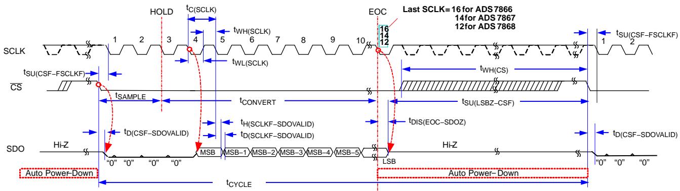
Fig u re 1 . Ti m i ng Diag ram
PIN CONFIGU RATION
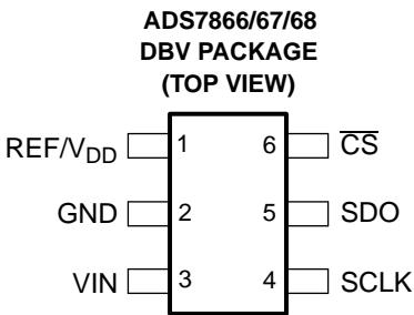
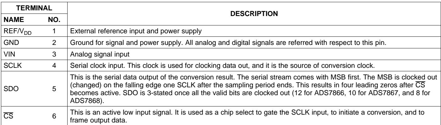
TERMINAL FUNCTIONS
| TERMINAL | DESCRIPTION | |
| NAME | NO. | |
| $REF/V_{DD}$ | 1 | External reference input and power supply |
| GND | 2 | Ground for signal and power supply. All analog and digital signals are referred with respect to this pin. |
| VIN | 3 | Analog signal input |
| SCLK | 4 | Serial clock input. This clock is used for clocking data out, and it is the source of conversion clock. |
| SDO | 5 | This is the serial data output of the conversion result. The serial stream comes with MSB first. The MSB is clocked out (changed) on the falling edge one SCLK after the sampling period ends. This results in four leading zeros after $\overline{CS}$ becomes active. SDO is 3-stated once all the valid bits are clocked out (12 for ADS7866, 10 for ADS7867, and 8 for ADS7868). |
| $\overline{CS}$ | 6 | This is an active low input signal. It is used as a chip select to gate the SCLK input, to initiate a conversion, and to frame output data. |
TYPICAL CHARACTERISTICS ADS7866 FFT (81 92 Poi nts)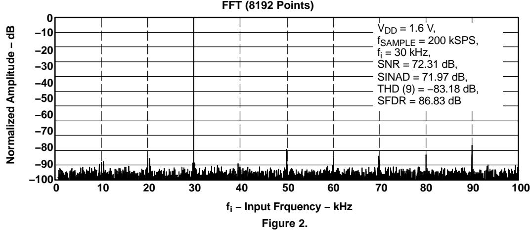
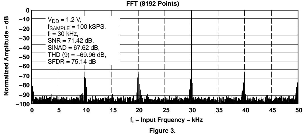
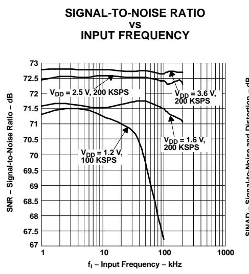
Fi g u re 4.
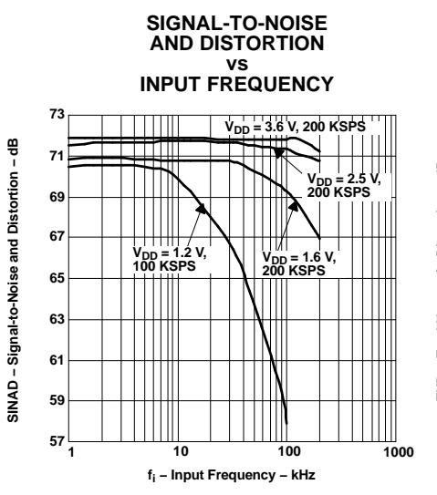
Fi g u re 5 .
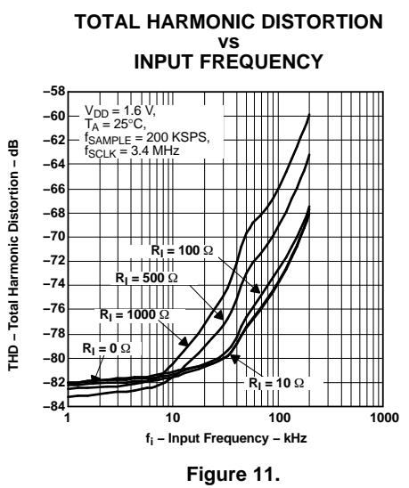
TOTAL HARMONIC DISTORTION vs INPUT FREQU ENCY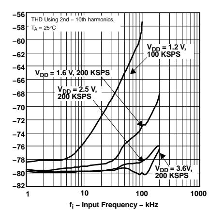
Fig u re 6.
TYPICAL CHARACTERISTICS ADS7866 (continued)
SPU RIOUS FREE DYNAMIC RANGE vs INPUT FREQU ENCY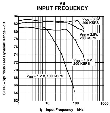
Fi g u re 7.
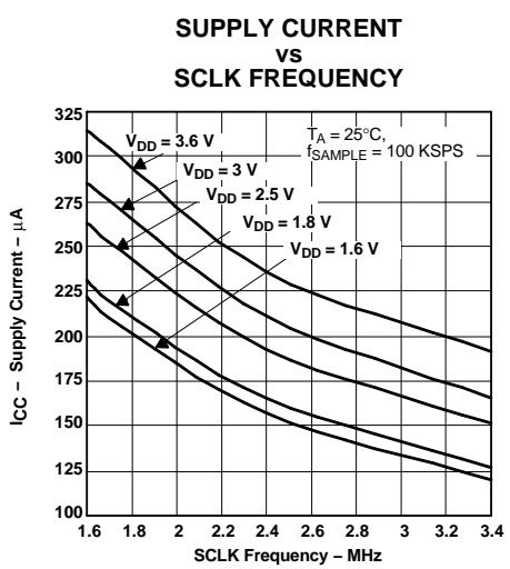
Fi g u re 8.
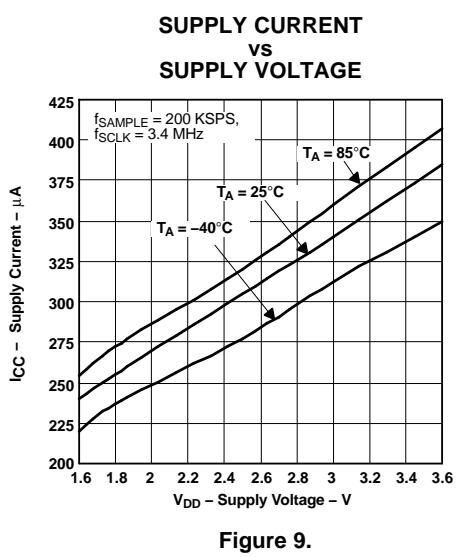
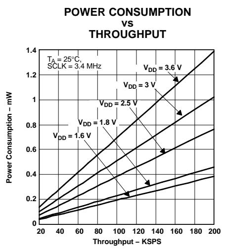
F i g u re 1 0 .
I N L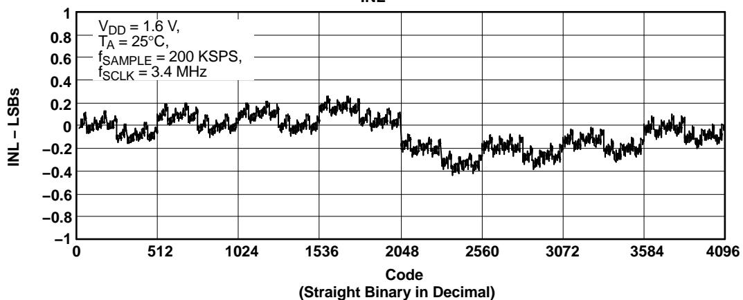
Fi g u re 1 2 .
DNL
TYPICAL CHARACTERISTICS ADS7866 (continued)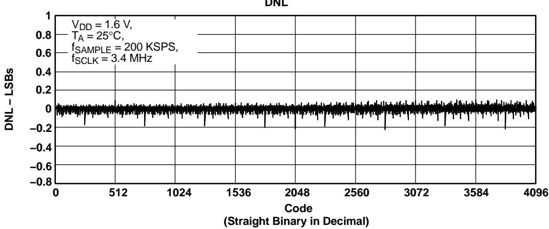
Fi g u re 1 3 .
I N L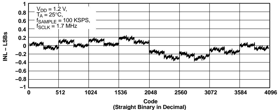
Fi g u re 1 4.
DNL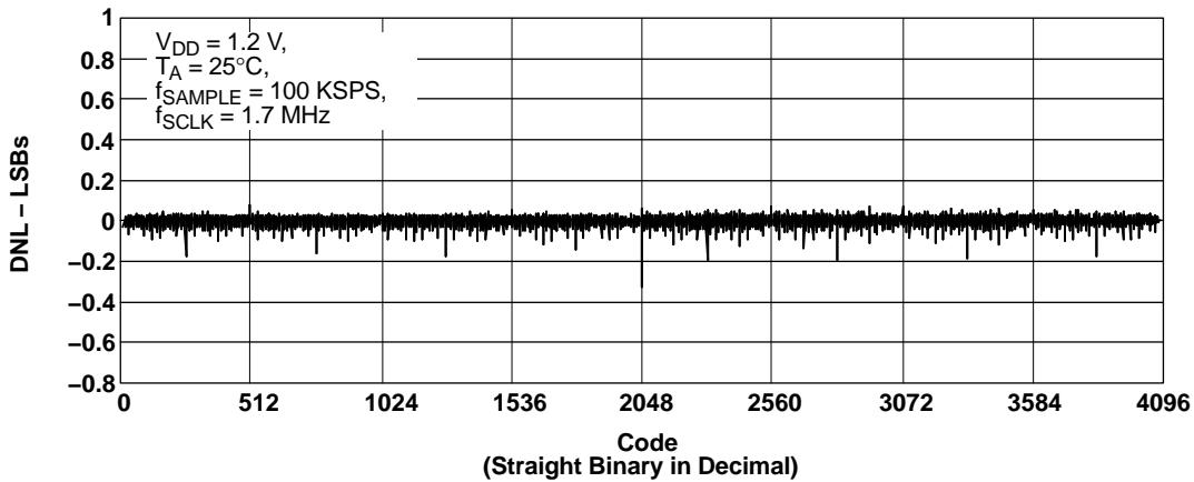
Fi g u re 1 5 .
TYPICAL CHARACTERISTICS ADS7866 (continued)
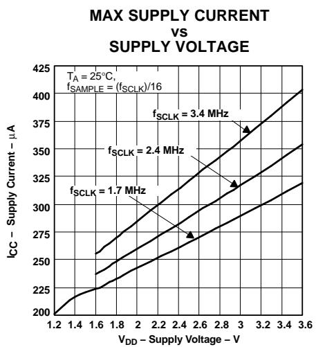
F i g u re 1 6 .
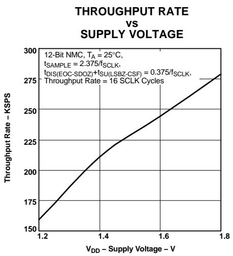
F i g u re 1 7 .
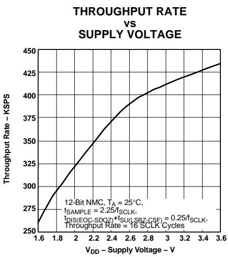
Fi g u re 1 8.
TYPICAL CHARACTERISTICS ADS7867 FFT (81 92 Poi nts)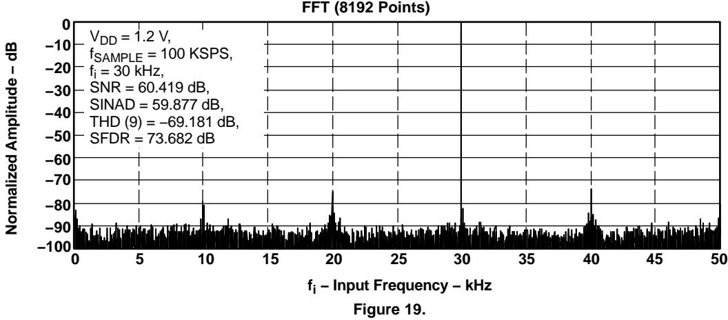
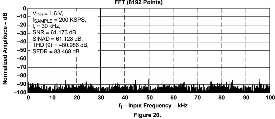
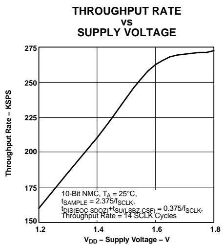
F i g u re 2 1 .
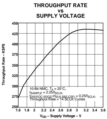
Fig u re 22.
FFT (81 92 Poi nts)
TYPICAL CHARACTERISTICS ADS7868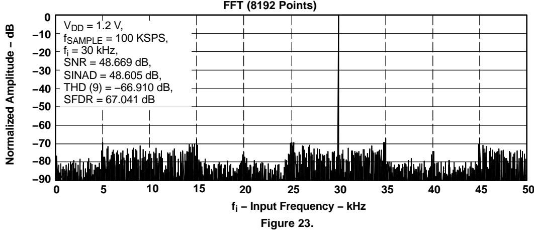
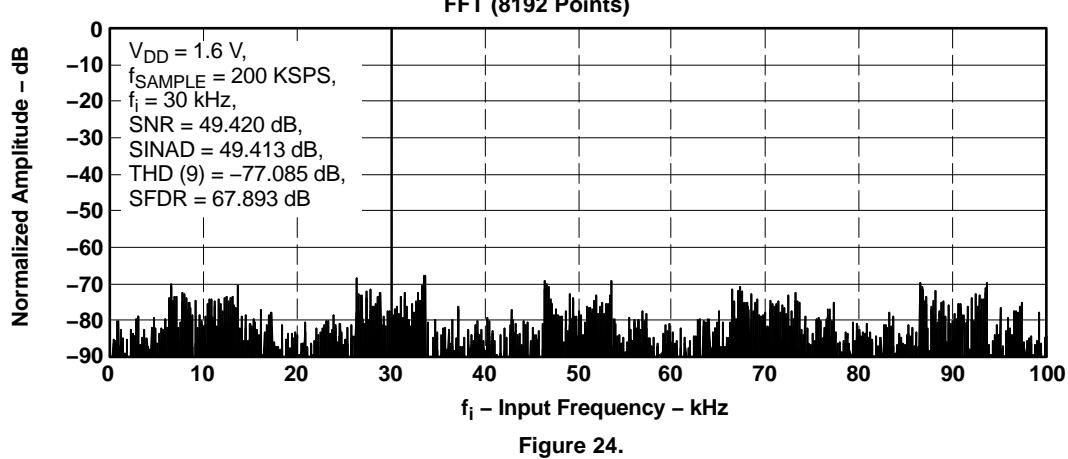
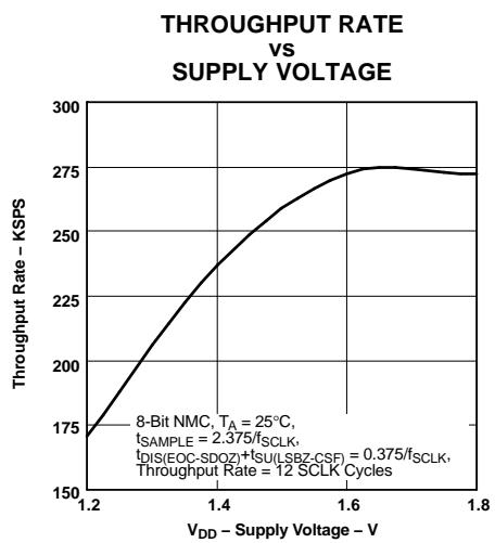
Fig u re 25.
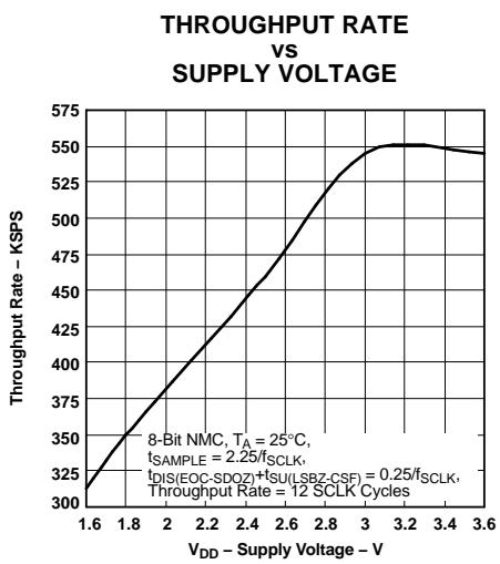
Fig u re 26.
TH EORY OF OPERATION
The ADS7866/67/68 is a fam i ly of low su pply voltage , low powe r, h ig h-speed successive app roxi mation reg iste r (SAR) analog-to-d ig ital conve rte rs (ADCs) The devices can be ope rated from a su pply range from 1 2 V to 3 6 V The re is no need fo r an exte rnal refe rence The refe rence is de rived i nte rnal ly from the su pply voltage so the analog i n put range can be from 0 V to $\mathsf { V } _ { \mathsf { D D } }$ These ADCs use a charge red istri bution arch itectu re wh ich i n he rently i ncl udes a sam pl e/hold fu nction
START OF A CONVERSION CYCLE
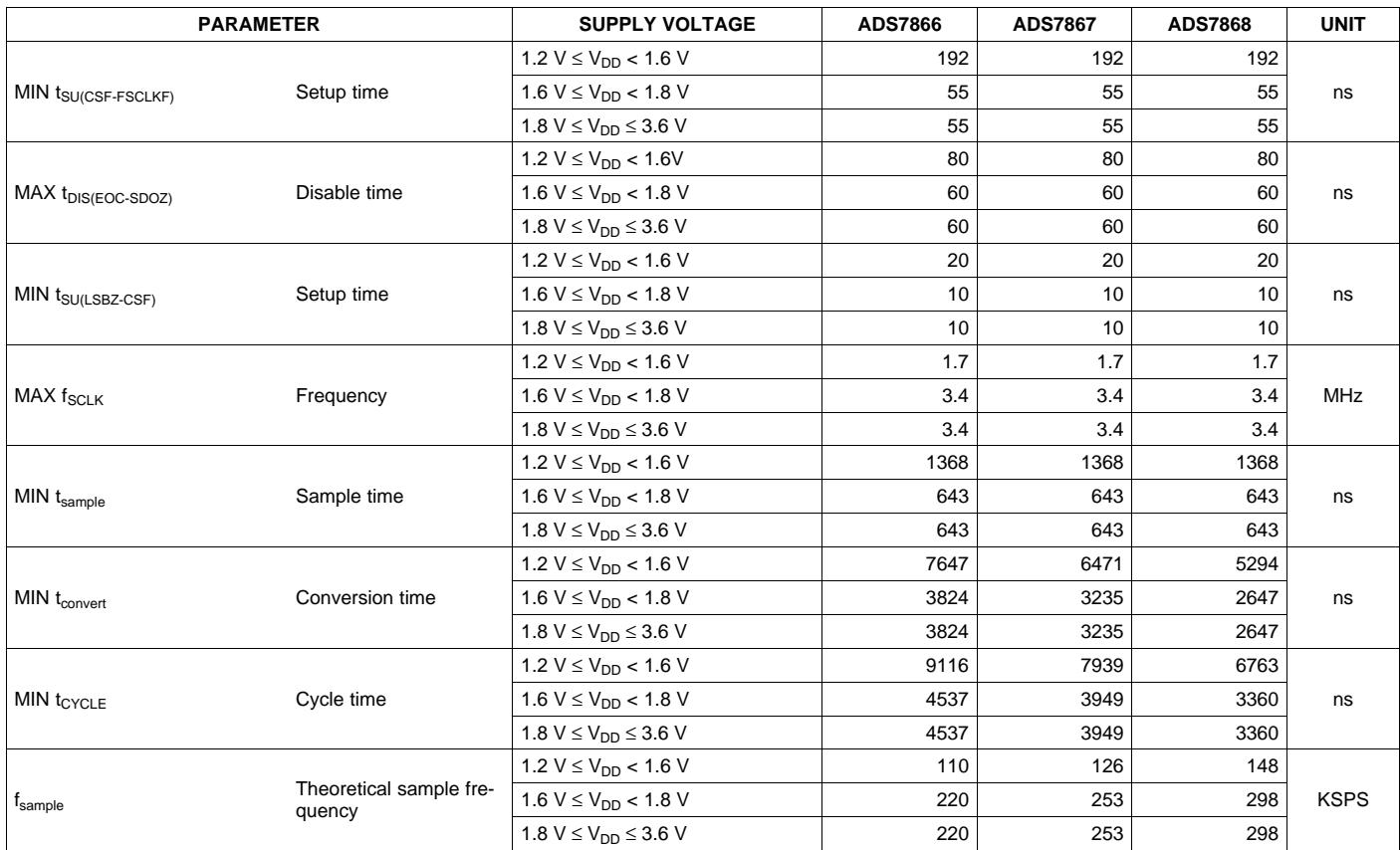
A conve rsion cycl e is i n itiated by b ri ng i ng the $\overline { { \mathsf { C S } } }$ pi n low and su pplyi ng the se rial clock SC LK. The ti me between the fal l i ng edge of CS and the th i rd fal l i ng edge of SC LK afte r CS fal ls is used to acq u i re the i n p ut si g nal . Th is m ust be g reate r than o r eq ual to the m i n i m u m acq u isition ti me ( M I N $\mathsf { t } _ { \mathsf { S A M P L E } }$ i n Table 1 ) specified fo r the desi red resol ution and su pply voltage On the th i rd fal l i ng edge of SC LK afte r CS fal ls the device goes i nto hold mode and the p rocess of d i g itizi ng the sam pl ed i n p ut si g nal starts .
Acqu isition Ti me Conversion Ti me and Total Cycle Ti me
The maxi m u m SC LK freq uency is dete rm i ned by the m i n i m u m acq u isition ti me (M I N $\mathfrak { t } _ { \mathsf { S A M P L E } } )$ specified fo r the specific resol ution and su pply voltage of the device . The conve rsion ti me is dete rm i ned by the freq uency of SC LK si nce th is is a synch ronous conve rte r The conve rsion ti me is 1 3 ti mes the SC LK cycle ti me $\mathsf { t } _ { \mathsf { C } ( \mathsf { S C L K } ) }$ fo r t h e ADS7866 1 1 ti mes for the ADS7867 and 9 ti mes for the ADS7868 The acq u isition ti me wh ich is also the powe r u p ti me is the set- u p ti me between the fi rst fal l i ng edge of SC LK afte r CS fal ls $( \tt t _ { S U ( C S F - F S C L K F ) } )$ pl us 2 t i m es tC(SC LK) .
The total cycle ti me $\mathsf { t } _ { \mathsf { C Y C L E } } ,$ wh ich is the i nve rse of the maxi m u m sam ple rate can be calcu lated as fol lows :
$$
t _ {C Y C L E} = t _ {S A M P L E} + t _ {C O N V E R T} + 0. 5 \times t _ {C (S C L K)}
$$
$$
i f t _ {D I S (E O C - S D O Z)} + t _ {S U (L S B Z - C S F)} \leq 0. 5 \times t _ {C (S C L K)}
$$
$$
t _ {\text { CYCLE }} = t _ {\text { SAMPLE }} + t _ {\text { CONVERT }} + t _ {\text { DIS(EOC - SDOZ) }} + t _ {\text { SU(LSBZ - CSF) }}
$$
$$
\mathrm {if t_ {DIS(EOC - SDOZ)} + t_ {SU(LSBZ - CSF)} > 0.5\times t_ {C(SCLK)}}
$$
TH EORY OF OPERATION (continued)
Table 1 . Acq u isition Conversion SCLK and Potential Th roug h put Calcu lation
| PARAMETER | SUPPLY VOLTAGE | ADS7866 | ADS7867 | ADS7868 | UNIT | |
| MIN tsU(CSF-FSCLKF) | Setup time | 1.2 V ≤ VDD< 1.6 V | 192 | 192 | 192 | ns |
| 1.6 V ≤ VDD< 1.8 V | 55 | 55 | 55 | |||
| 1.8 V ≤ VDD≤ 3.6 V | 55 | 55 | 55 | |||
| MAX tDIS(EOC-SDOZ) | Disable time | 1.2 V ≤ VDD< 1.6V | 80 | 80 | 80 | ns |
| 1.6 V ≤ VDD< 1.8 V | 60 | 60 | 60 | |||
| 1.8 V ≤ VDD≤ 3.6 V | 60 | 60 | 60 | |||
| MIN tsU(LSBZ-CSF) | Setup time | 1.2 V ≤ VDD< 1.6 V | 20 | 20 | 20 | ns |
| 1.6 V ≤ VDD< 1.8 V | 10 | 10 | 10 | |||
| 1.8 V ≤ VDD≤ 3.6 V | 10 | 10 | 10 | |||
| MAX fsCLK | Frequency | 1.2 V ≤ VDD< 1.6 V | 1.7 | 1.7 | 1.7 | MHz |
| 1.6 V ≤ VDD< 1.8 V | 3.4 | 3.4 | 3.4 | |||
| 1.8 V ≤ VDD≤ 3.6 V | 3.4 | 3.4 | 3.4 | |||
| MIN tsample | Sample time | 1.2 V ≤ VDD< 1.6 V | 1368 | 1368 | 1368 | ns |
| 1.6 V ≤ VDD< 1.8 V | 643 | 643 | 643 | |||
| 1.8 V ≤ VDD≤ 3.6 V | 643 | 643 | 643 | |||
| MIN tconvert | Conversion time | 1.2 V ≤ VDD< 1.6 V | 7647 | 6471 | 5294 | ns |
| 1.6 V ≤ VDD< 1.8 V | 3824 | 3235 | 2647 | |||
| 1.8 V ≤ VDD≤ 3.6 V | 3824 | 3235 | 2647 | |||
| MIN tCYCLE | Cycle time | 1.2 V ≤ VDD< 1.6 V | 9116 | 7939 | 6763 | ns |
| 1.6 V ≤ VDD< 1.8 V | 4537 | 3949 | 3360 | |||
| 1.8 V ≤ VDD≤ 3.6 V | 4537 | 3949 | 3360 | |||
| fsample | Theoretical sample frequency | 1.2 V ≤ VDD< 1.6 V | 110 | 126 | 148 | KSPS |
| 1.6 V ≤ VDD< 1.8 V | 220 | 253 | 298 | |||
| 1.8 V ≤ VDD≤ 3.6 V | 220 | 253 | 298 | |||
TYPICAL CONNECTION
For a typical con nection ci rcu it for the ADS7866/67/68 see Fig u re 27. A R E F3 1 1 2 is used to su pply 1 .2 V to the device A 0 1 -µ F decou pl i ng capacitor is req u i red between the $\mathsf { R E F } N _ { \mathsf { D D } }$ and G N D pi ns of the conve rte r. Th is capacito r shou ld be placed as close as possi ble to the pi ns of the device . Desig ne rs shou ld strive to m i n i m ize the routi ng l ength of the traces that con nect the te rm i nals of the capacito r to the pi ns of the conve rte r.
Keep i n m i nd the conve rte r offe rs no i n he rent rejection of noise o r voltage variation i n regards to the refe rence i n put . Th is is of particu lar conce rn because the refe rence i n put is tied to the powe r su pply. Any noise and ri pple from the su pply appears d i rectly i n the d ig ital resu lts . Wh i le h ig h freq uency noise can be fi lte red out as descri bed i n the p revious parag raph voltage variation d ue to the l i ne freq uency (50 Hz o r 60 Hz) can be d ifficu lt to remove
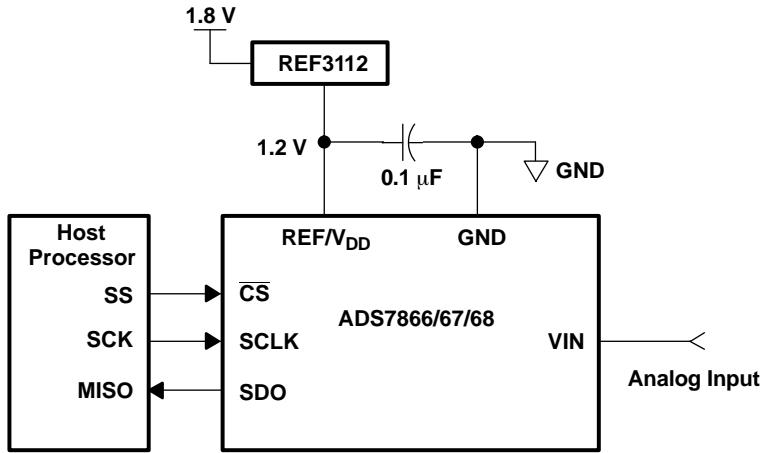
Fig u re 27. Typical Ci rcu it Config u ration
ANALOG INPUT
Fig u re 28 shows the analog i n put eq u ivalent ci rcu it for the ADS7866/67/68 The analog i n put is p rovided between the V I N and G N D pi ns . When a conve rsion is i n itiated the i n put sig nal is sam pled on the i nte rnal capacito r array When the conve rte r ente rs hold mode the i n put sig nal is captu red on the i nte rnal capacito r array. The V I N i n put range is l i m ited to 0 V to $\mathsf { V } _ { \mathsf { D D } }$ because the refe rence is de rived from the su pply.
The cu rrent flowi ng i nto the analog i n put depends u pon a n u m be r of facto rs such as the sam ple rate the i n put voltage and the i n put sou rce i m pedance The cu rrent from the i n put sou rce charges the i nte rnal capacito r array d u ri ng the sam pl e pe riod . Afte r th is capacitance has been fu l ly charged the re is no fu rthe r i n p ut cu rrent . The sou rce of the analo i n ut volta e m ust be able to char e the i n ut ca acitance ${ \sf C } _ { \sf S }$ ( 1 2 p F typi cal) with i n the m i n i m u m acq u isition ti me ( M I N $\mathfrak { t } _ { \mathsf { S A M P L E } } )$ specified fo r the desi red resol ution and su pply voltage . I n the case of the ADS7866 the M I N $\mathsf { t } _ { \mathsf { S A M P L E } }$ fo r 1 2-bit resol ution is 643 ns $( \mathsf { V } _ { \mathsf { D } \mathsf { D } }$ between 1 6 V and 3 6 V) When the converter goes i nto hold mode the i n put i m pedance is g reate r than 1 GΩ
Care m ust be taken regard i ng the absol ute analog i n put voltage . I n o rde r to mai ntai n the l i nearity of the conve rte r the span (V I N – G N D) shou ld be with i n the l i m its specified . Outside of these l i m its the conve rte r’s l i nearity may not meet specifications . N oise i ntrod uced i nto the conve rte r from the i n put sou rce may be m i n i m ized by usi ng low bandwidth i n put sig nals along with low-pass fi lte rs
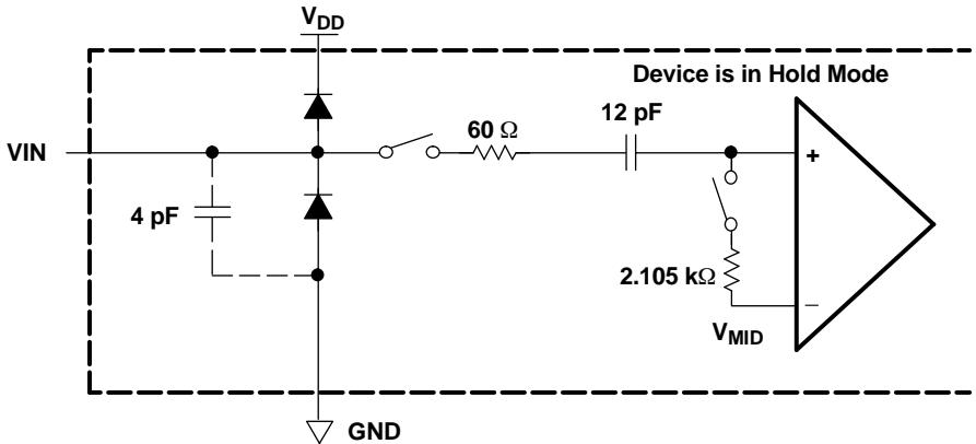
Fig u re 28. Analog I n put Eq u ivalent Ci rcu it (Typical I m pedance Val ues at $\mathsf { V } _ { \mathsf { D D } } = 1 . 6 \ \mathsf { V } , \mathsf { T } _ { \mathsf { A } } = 2 7 ^ { \circ } \mathsf { C } )$
Choice of I n put Drivi ng Am pl ifier
The analog i n put to the conve rte r needs to be d riven with a low noise low voltage op am p l i ke the O PA364 or O PA333 An RC fi lte r is recom mended at the i n put pi n to low-pass fi lte r the noise from the sou rce The i n put to the conve rte r is a u n i polar i n p ut voltage i n the range 0 V to $\mathsf { V } _ { \mathsf { D D } }$
DIGITAL INTERFACE
The ADS7866/67/68 i nte rface with m icrop rocessors or DS Ps th roug h a h ig h-speed S P I com pati ble se rial i nte rface with C PO L = 1 (i nactive SC LK retu rns to log ic h ig h or SC LK lead i ng edge is the risi ng edge) C P HA = 1 (output data changes on fal l i ng edge of SC LK and is avai lable on the risi ng edge of SC LK) The sam pl i ng conve rsion and activation of S DO are i n itiated on the fal l i ng edge of CS . The se rial clock (SC LK) is used fo control l i ng the rate of conve rsion . It also p rovides a mechan ism al lowi ng synch ron ization with d ig ital host p rocesso rs .
The d ig ital i n puts CS and SC LK can exceed the su pply voltage $\mathsf { V } _ { \mathsf { D D } }$ as long as they do not exceed the maxi m u m $\mathsf { V } _ { \mathsf { H } }$ of 3 6 V Th is al lows the ADS7866/67/68 fam i ly to i nte rface with host p rocesso rs wh ich use a d iffe rent su pply voltage than the conve rte r without req u i ri ng exte rnal l eve l -sh ifti ng ci rcu itry. Fu rthe rmo re the d ig ital i n puts can be appl ied to CS and SC LK before the su pply voltage of the conve rte r is activated without the risk of creati ng a latch - u p cond ition .
Conversion Resu lt
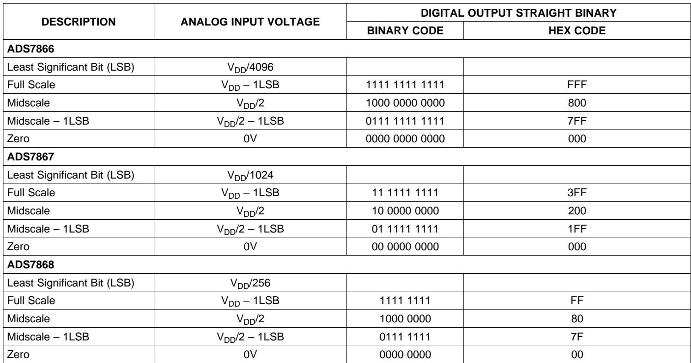
The ADS7866/67/68 outputs 1 2/1 0/8-bit data afte r 4 lead i ng ze ros respectively These codes are i n straig ht bi nary fo rmat as shown i n Table 2 .
The se rial output S DO is activated on the fal l i ng edge of CS . The fi rst lead i ng ze ro is avai lable on S DO u nti l the fi rst fal l i ng edge of SC LK afte r CS fal ls . The remai n i ng 3 lead i ng ze ros are sh ifted out on S DO on the fi rst second and th i rd fal l i ng edges of SC LK afte r CS fal ls . The M S B of the conve rted resu lt fol lows 4 lead i ng ze ros and is clocked out on the fou rth fal l i ng edge of SC LK. The risi ng edge of CS or the fal l i ng edge of SC LK when the E OC occu rs puts S DO output i nto 3-state . Refe r to Table 2 fo r ideal output codes ve rsus i n put voltages .
Table 2. ADS7866/67/68 Ideal Output Codes Versus I n put Voltages
| DESCRIPTION | ANALOG INPUT VOLTAGE | DIGITAL OUTPUT STRAIGHT BINARY | |
| BINARY CODE | HEX CODE | ||
| ADS7866 | |||
| Least Significant Bit (LSB) | $V_{DD}/4096$ | ||
| Full Scale | $V_{DD}-1LSB$ | 1111 1111 1111 | FFF |
| Midscale | $V_{DD}/2$ | 1000 0000 0000 | 800 |
| Midscale - 1LSB | $V_{DD}/2-1LSB$ | 0111 1111 1111 | 7FF |
| Zero | 0V | 0000 0000 0000 | 000 |
| ADS7867 | |||
| Least Significant Bit (LSB) | $V_{DD}/1024$ | ||
| Full Scale | $V_{DD}-1LSB$ | 11 1111 1111 | 3FF |
| Midscale | $V_{DD}/2$ | 10 0000 0000 | 200 |
| Midscale - 1LSB | $V_{DD}/2-1LSB$ | 01 1111 1111 | 1FF |
| Zero | 0V | 00 0000 0000 | 000 |
| ADS7868 | |||
| Least Significant Bit (LSB) | $V_{DD}/256$ | ||
| Full Scale | $V_{DD}-1LSB$ | 1111 1111 | FF |
| Midscale | $V_{DD}/2$ | 1000 0000 | 80 |
| Midscale - 1LSB | $V_{DD}/2-1LSB$ | 0111 1111 | 7F |
| Zero | 0V | 0000 0000 | 00 |
POWER DISSIPATION
The ADS7866/67/68 fam i ly is capable of ope rati ng with ve ry low su pply voltages wh i le d rawi ng a fraction of a m i l l iam p Fu rthe rmore the re is an auto powe r-down mode to red uce the powe r d issi pation between conve rsion cycles Carefu l ly selected system desig n can take advantage of these featu res to ach ieve opti m u m powe r pe rformance .
Auto Power-Down Mode
The ADS7866/67/68 fam i ly has an auto powe r-down featu re Besides powe ri ng down al l ci rcu itry the conve rte r consu mes on ly 8 nA typical ly i n th is mode The device automatical ly wakes u p when CS fal ls Howeve r not al l of the fu nctional blocks are fu l ly powe red u nti l someti me befo re the th i rd fal l i ng edge of SC LK The device powe rs down once it reaches the end of conve rsion ( E OC) wh ich is the 1 6th fal l i ng edge of SC LK fo r the ADS7866 (the 1 4th and 1 2th for the ADS7867 and ADS7868 respectively) If CS is pu l led h ig h before the device reaches the E OC the conve rte r goes i nto powe r-down mode and the ongoi ng conve rsion is aborted . Refe r to the ti m i ng d iag ram i n Fi g u re 1 fo r fu rthe r i nfo rmation
Power Savi ng : SCLK Freq uency and Th rough put
These conve rte rs ach ieve lowe r powe r d issi pation fo r a fixed th roug h put rate $\mathsf { f } _ { \mathsf { s a m p l e } } = 1 / \mathsf { t } _ { \mathsf { c y c l e } }$ by usi ng h i g he r SC LK freq uencies H ig he r SC LK freq uencies red uce the acq u isition ti me $( \mathsf { t } _ { \mathsf { s a m p l e } } )$ and conve rsion ti me $( \mathfrak { t } _ { \mathtt { c o n v e r t } } )$ Th is means the conve rte rs spend more ti me i n auto powe r-down mode pe r conve rsion cycle Th is can be obse rved i n Fig u re 8 wh ich shows the ADS7866 su pply cu rrent ve rsus SC LK freq uency for $\mathsf { f } _ { \mathsf { s a m p l e } } = 1 0 0 ~ \mathsf { K S P S }$ Fo r a particu lar SC LK freq uency the acq u isition ti me and conve rsion ti me are fixed The refo re a lowe r th roug h put i ncreases the p ropo rtion of the ti me the conve rte rs are i n powe r down Fig u re 1 0 shows th is case fo r the ADS7866 powe r consu m ption ve rsus th roug h put rate fo r $\mathsf { f } _ { \mathsf { S C L K } } = 3 . 4 ~ \mathsf { M H z }$
Power-On I n itial ization
The re is no specifi c i n itial ization req u i rement fo r these conve rte rs afte r powe r-on b ut the fi rst conve rsion m i g ht not yield a val id resu lt. I n o rde r to set the conve rte r i n a known state CS shou ld be togg led low then h ig h afte r $\mathsf { V } _ { \mathsf { D D } }$ has stabi l ized d u ri ng powe r-on . By doi ng th is the conve rte r is placed i n auto powe r-down mode and the se rial data output (S DO) is 3-stated
PACKAGING INFORMATION
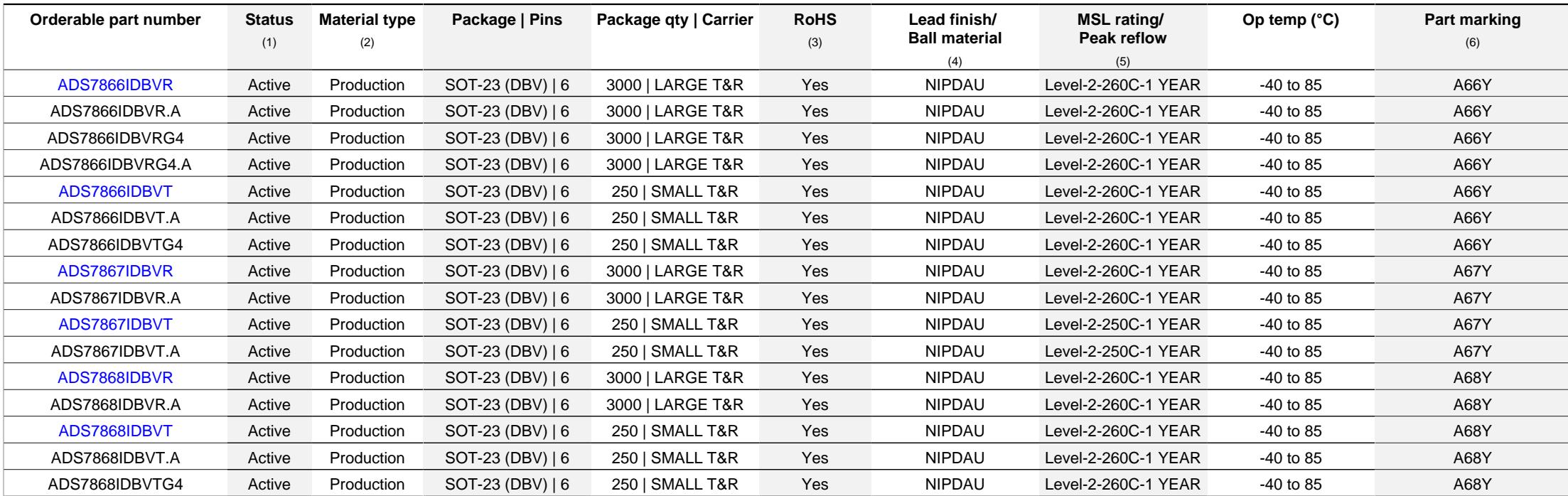
| Orderable part number | Status(1) | Material type(2) | Package | Pins | Package qty | Carrier | RoHS(3) | Lead finish/ Ball material(4) | MSL rating/ Peak reflow(5) | Op temp (°C) | Part marking(6) |
| ADS7866IDBVR | Active | Production | SOT-23 (DBV) | 6 | 3000 | LARGE T&R | Yes | NIPDAU | Level-2-260C-1 YEAR | -40 to 85 | A66Y |
| ADS7866IDBVR.A | Active | Production | SOT-23 (DBV) | 6 | 3000 | LARGE T&R | Yes | NIPDAU | Level-2-260C-1 YEAR | -40 to 85 | A66Y |
| ADS7866IDBVRG4 | Active | Production | SOT-23 (DBV) | 6 | 3000 | LARGE T&R | Yes | NIPDAU | Level-2-260C-1 YEAR | -40 to 85 | A66Y |
| ADS7866IDBVRG4.A | Active | Production | SOT-23 (DBV) | 6 | 3000 | LARGE T&R | Yes | NIPDAU | Level-2-260C-1 YEAR | -40 to 85 | A66Y |
| ADS7866IDBVT | Active | Production | SOT-23 (DBV) | 6 | 250 | SMALL T&R | Yes | NIPDAU | Level-2-260C-1 YEAR | -40 to 85 | A66Y |
| ADS7866IDBVT.A | Active | Production | SOT-23 (DBV) | 6 | 250 | SMALL T&R | Yes | NIPDAU | Level-2-260C-1 YEAR | -40 to 85 | A66Y |
| ADS7866IDBVTG4 | Active | Production | SOT-23 (DBV) | 6 | 250 | SMALL T&R | Yes | NIPDAU | Level-2-260C-1 YEAR | -40 to 85 | A66Y |
| ADS7867IDBVR | Active | Production | SOT-23 (DBV) | 6 | 3000 | LARGE T&R | Yes | NIPDAU | Level-2-260C-1 YEAR | -40 to 85 | A67Y |
| ADS7867IDBVR.A | Active | Production | SOT-23 (DBV) | 6 | 3000 | LARGE T&R | Yes | NIPDAU | Level-2-260C-1 YEAR | -40 to 85 | A67Y |
| ADS7867IDBVT | Active | Production | SOT-23 (DBV) | 6 | 250 | SMALL T&R | Yes | NIPDAU | Level-2-250C-1 YEAR | -40 to 85 | A67Y |
| ADS7867IDBVT.A | Active | Production | SOT-23 (DBV) | 6 | 250 | SMALL T&R | Yes | NIPDAU | Level-2-250C-1 YEAR | -40 to 85 | A67Y |
| ADS7868IDBVR | Active | Production | SOT-23 (DBV) | 6 | 3000 | LARGE T&R | Yes | NIPDAU | Level-2-260C-1 YEAR | -40 to 85 | A68Y |
| ADS7868IDBVR.A | Active | Production | SOT-23 (DBV) | 6 | 3000 | LARGE T&R | Yes | NIPDAU | Level-2-260C-1 YEAR | -40 to 85 | A68Y |
| ADS7868IDBVT | Active | Production | SOT-23 (DBV) | 6 | 250 | SMALL T&R | Yes | NIPDAU | Level-2-260C-1 YEAR | -40 to 85 | A68Y |
| ADS7868IDBVT.A | Active | Production | SOT-23 (DBV) | 6 | 250 | SMALL T&R | Yes | NIPDAU | Level-2-260C-1 YEAR | -40 to 85 | A68Y |
| ADS7868IDBVTG4 | Active | Production | SOT-23 (DBV) | 6 | 250 | SMALL T&R | Yes | NIPDAU | Level-2-260C-1 YEAR | -40 to 85 | A68Y |
(1) Status: For more details on status, see our product life cycle.
(6) Part marking: There may be an additional marking, which relates to the logo, the lot trace code information, or the environmental category of the part.
Multiple part markings will be inside parentheses. Only one part marking contained in parentheses and separated by a "~" will appear on a part. If a line is indented then it is a continuation of the previous line and the tw combined represent the entire part marking for that device
Important Information and Disclaimer:The information provided on this page represents TI's knowledge and belief as of the date that it is provided. TI bases its knowledge and belief on information provided by third parties, an makes no representation or warranty as to the accuracy of such information. Efforts are underway to better integrate information from third parties. TI has taken and continues to take reasonable steps to provide representativ and accurate information but may not have conducted destructive testing or chemical analysis on incoming materials and chemicals. TI and TI suppliers consider certain information to be proprietary, and thus CAS number and other limited information may not be available for release.
In no event shall TI's liability arising out of such information exceed the total purchase price of the TI part(s) at issue in this document sold by TI to Customer on an annual basis.
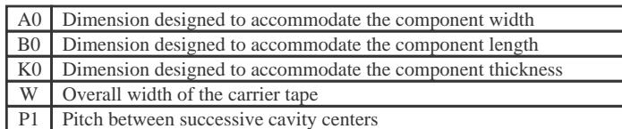
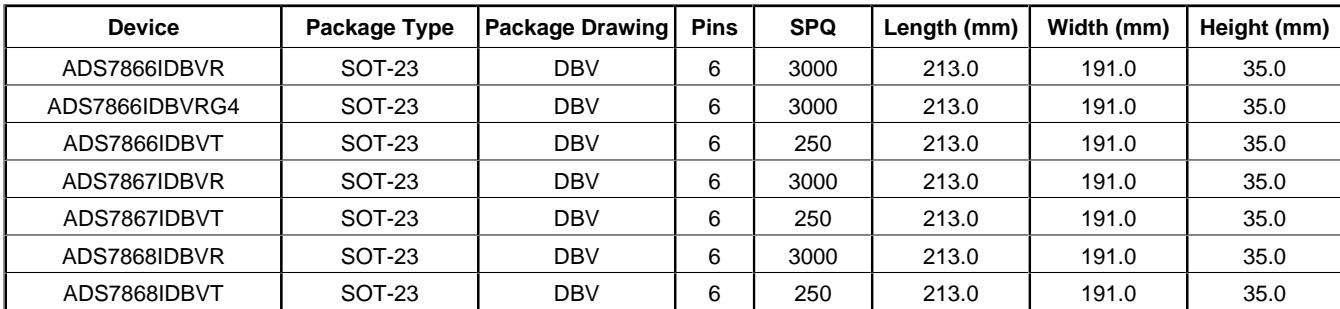
TAPE AND REEL INFORMATION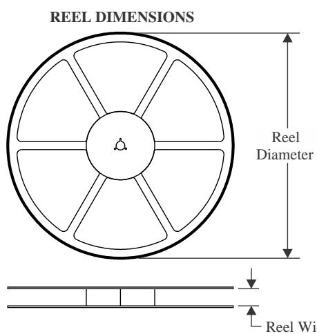
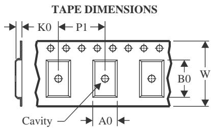
| A0 | Dimension designed to accommodate the component width |
| B0 | Dimension designed to accommodate the component length |
| K0 | Dimension designed to accommodate the component thickness |
| W | Overall width of the carrier tape |
| P1 | Pitch between successive cavity centers |
Reel Width (W1)
QUADRANT ASSIGNMENTS FOR PIN 1 ORIENTATION IN TAPE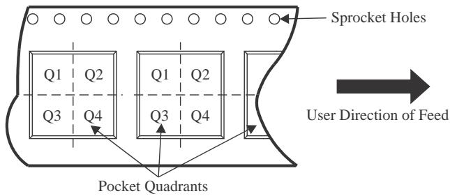
*All dimensions are nomina
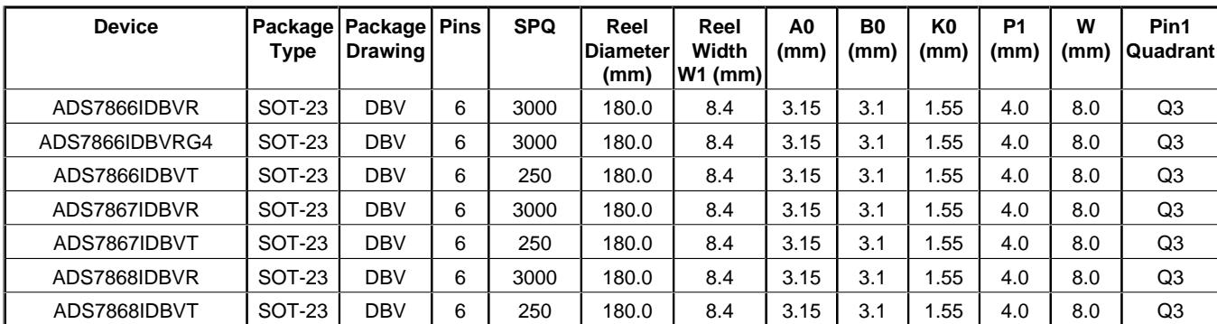
| Device | Package Type | Package Drawing | Pins | SPQ | Reel Diameter (mm) | Reel Width W1 (mm) | A0 (mm) | B0 (mm) | K0 (mm) | P1 (mm) | W (mm) | Pin1 Quadrant |
| ADS7866IDBVR | SOT-23 | DBV | 6 | 3000 | 180.0 | 8.4 | 3.15 | 3.1 | 1.55 | 4.0 | 8.0 | Q3 |
| ADS7866IDBVRG4 | SOT-23 | DBV | 6 | 3000 | 180.0 | 8.4 | 3.15 | 3.1 | 1.55 | 4.0 | 8.0 | Q3 |
| ADS7866IDBVT | SOT-23 | DBV | 6 | 250 | 180.0 | 8.4 | 3.15 | 3.1 | 1.55 | 4.0 | 8.0 | Q3 |
| ADS7867IDBVR | SOT-23 | DBV | 6 | 3000 | 180.0 | 8.4 | 3.15 | 3.1 | 1.55 | 4.0 | 8.0 | Q3 |
| ADS7867IDBVT | SOT-23 | DBV | 6 | 250 | 180.0 | 8.4 | 3.15 | 3.1 | 1.55 | 4.0 | 8.0 | Q3 |
| ADS7868IDBVR | SOT-23 | DBV | 6 | 3000 | 180.0 | 8.4 | 3.15 | 3.1 | 1.55 | 4.0 | 8.0 | Q3 |
| ADS7868IDBVT | SOT-23 | DBV | 6 | 250 | 180.0 | 8.4 | 3.15 | 3.1 | 1.55 | 4.0 | 8.0 | Q3 |
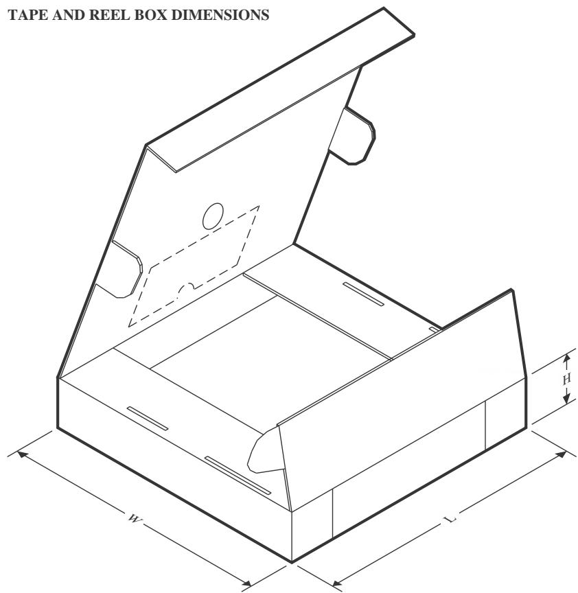
*All dimensions are nominal
| Device | Package Type | Package Drawing | Pins | SPQ | Length (mm) | Width (mm) | Height (mm) |
| ADS7866IDBVR | SOT-23 | DBV | 6 | 3000 | 213.0 | 191.0 | 35.0 |
| ADS7866IDBVRG4 | SOT-23 | DBV | 6 | 3000 | 213.0 | 191.0 | 35.0 |
| ADS7866IDBVT | SOT-23 | DBV | 6 | 250 | 213.0 | 191.0 | 35.0 |
| ADS7867IDBVR | SOT-23 | DBV | 6 | 3000 | 213.0 | 191.0 | 35.0 |
| ADS7867IDBVT | SOT-23 | DBV | 6 | 250 | 213.0 | 191.0 | 35.0 |
| ADS7868IDBVR | SOT-23 | DBV | 6 | 3000 | 213.0 | 191.0 | 35.0 |
| ADS7868IDBVT | SOT-23 | DBV | 6 | 250 | 213.0 | 191.0 | 35.0 |
4214840/G 08/2024
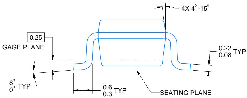
NOTES:
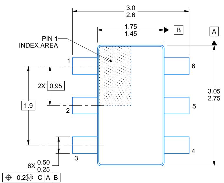
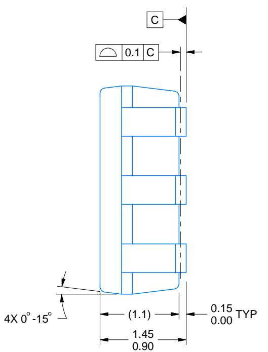
All linear dimensions are in millimeters. Any dimensions in parenthesis are for reference only. Dimensioning and tolerancing per ASME Y14.5M.
This drawing is subject to change without notice.
Body dimensions do not include mold flash or protrusion. Mold flash and protrusion shall not exceed 0.25 per side.
Leads 1,2,3 may be wider than leads 4,5,6 for package orientation.
Refernce JEDEC MO-178.
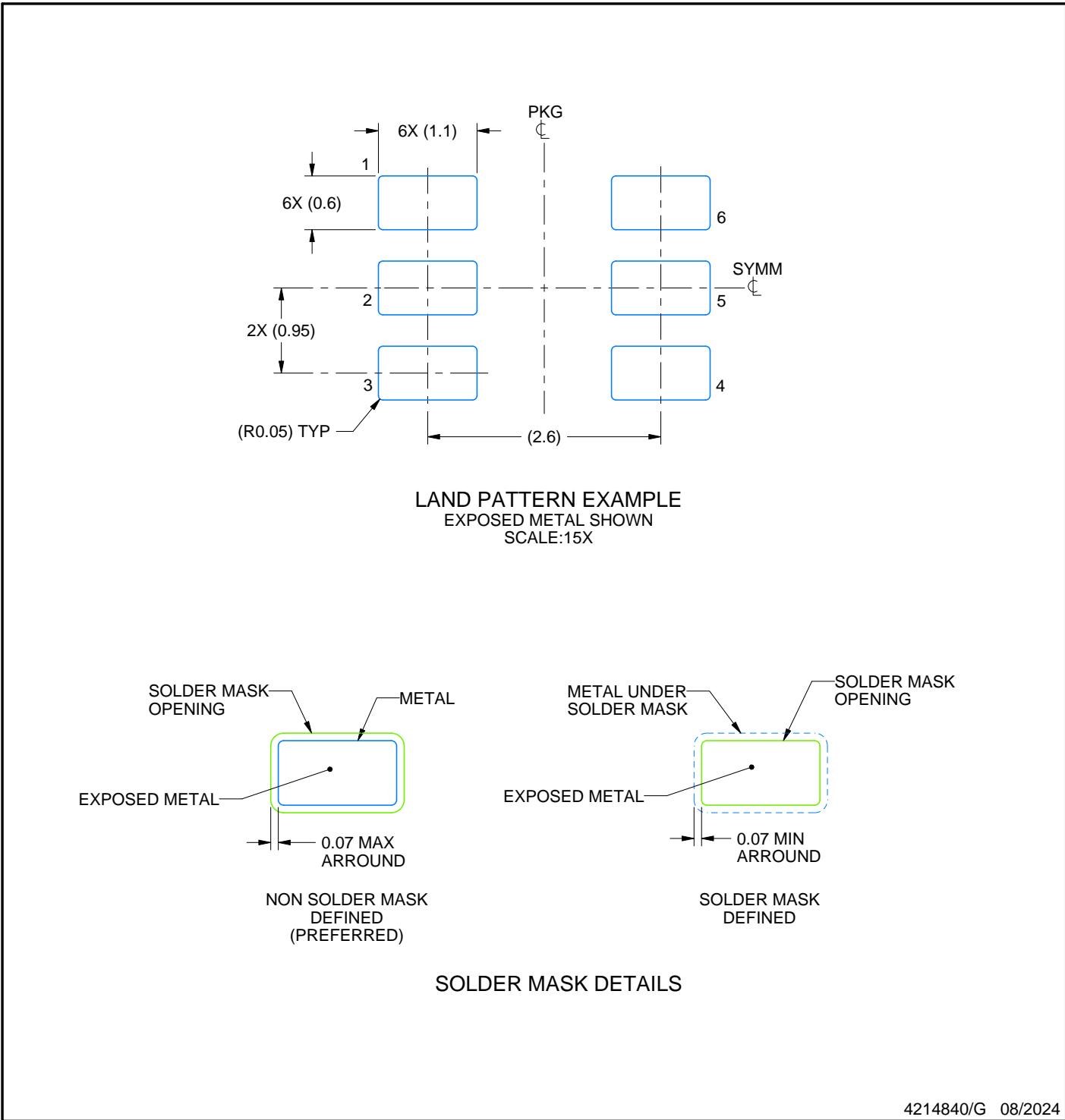
NOTES: (continued)
Publication IPC-7351 may have alternate designs.
Solder mask tolerances between and around signal pads can vary based on board fabrication site.
SMALL OUTLINE TRANSISTOR
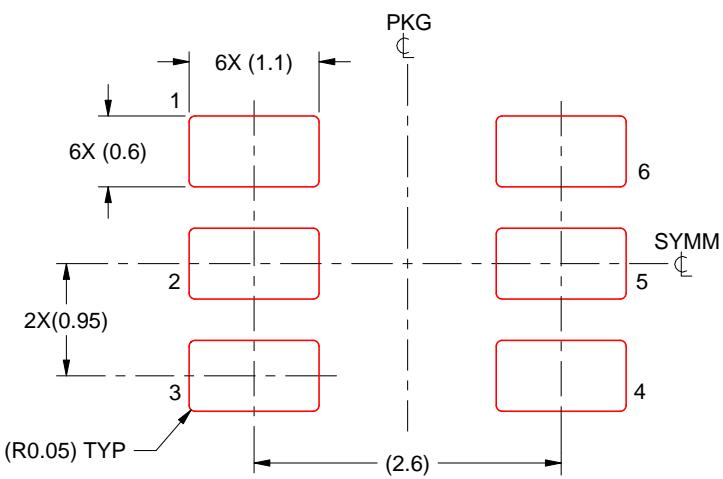
SOLDER PASTE EXAMPLE BASED ON 0.125 mm THICK STENCIL SCALE:15X
4214840/G 08/2024
NOTES: (continued)
Laser cutting apertures with trapezoidal walls and rounded corners may offer better paste release. IPC-7525 may have alternate design recommendations.
Board assembly site may have different recommendations for stencil design.
Figures and diagrams from the PDF
Preview the extracted datasheet assets and open any image in a separate tab for closer inspection.






Use this datasheet from any agent
Send the page, markdown, chunks, or search endpoint to ChatGPT, Claude, embedr-app, or your own tooling.