
B2B-PH-K-S
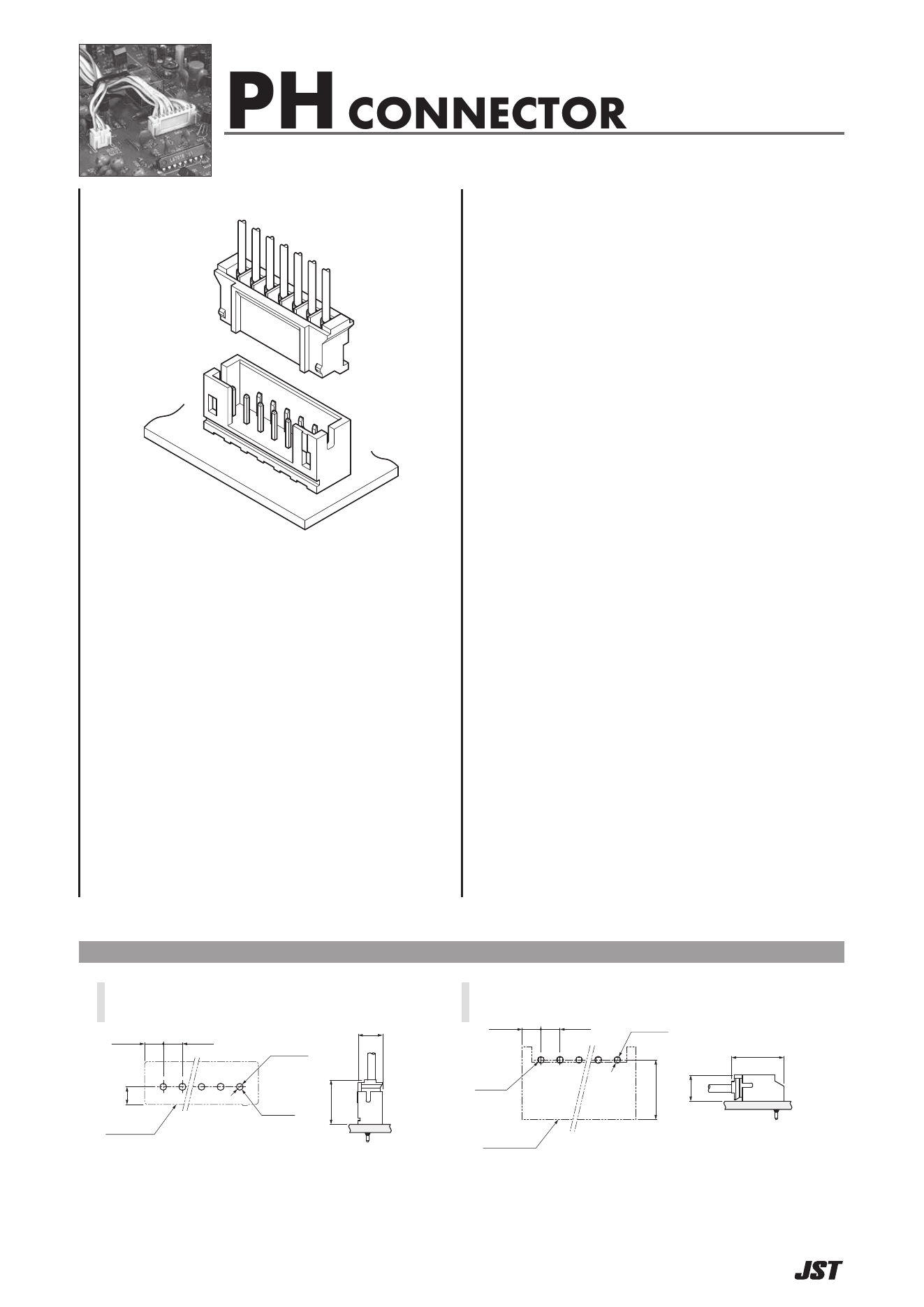
2-circuit, 2.00 mm-pitch, top-entry, through-hole wire-to-board header with friction lock.
JST PH series — B2B-PH-K-S
Identity and scope
- Manufacturer: J.S.T. Mfg. Co., Ltd.
- Exact part number: B2B-PH-K-S.
- This part is the 2-circuit, 2.00 mm-pitch, top-entry, through-hole PH-series board header. The
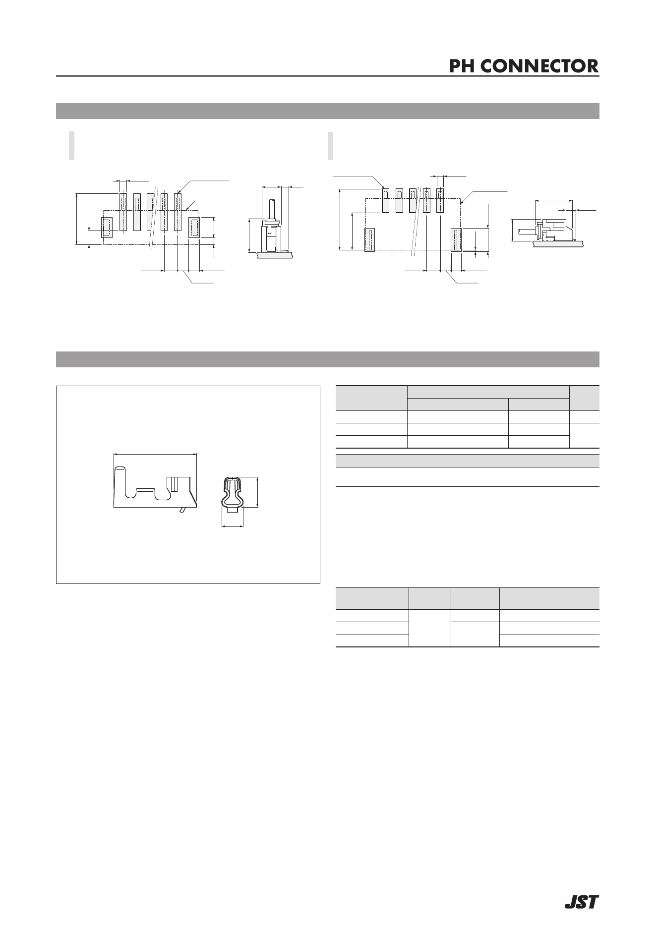
S2B-PH-K-Spart is the side-entry counterpart;B2B-PH-SM4-TBis the SMT counterpart and is not interchangeable with this record. - The PH series is a friction-lock wire-to-board connector family. The mating receptacle for this 2-circuit header is the JST PHR-2 housing (page 3 housing table: A 2.0 mm, B 5.8 mm), crimped with SPH-002T-P0.5S (AWG #30–#24, insulation O.D. 0.8–1.5 mm), SPH-004T-P0.5S (AWG #32–#28, insulation O.D. 0.5–0.9 mm), or the low-insertion-force SPH-002T-P0.5L (AWG #28–#24, insulation O.D. 0.8–1.5 mm) contacts (page 2 contact table).
Electrical limits and environment
- Rated current: 2 A AC/DC when using AWG #24 wire.
- Rated voltage: 100 V AC/DC.
- Temperature range: −40 to +105 °C, including the temperature rise from current flow.
- Initial contact resistance is 10 mΩ maximum; after environmental testing it is 20 mΩ maximum.
- Insulation resistance is 1,000 MΩ minimum. Dielectric withstand is 800 VAC for 1 minute.
- The specified wire range is AWG #32–#24 with insulation outside diameter 0.5–1.5 mm. These are connector-family limits; select wire, mating housing, and system protection for the actual design.
PCB and mechanical information
- The top-entry header uses two plated through-holes on a 2.00 ±0.05 mm pitch. The recommended hole diameter is 0.7 +0.1/0 mm.
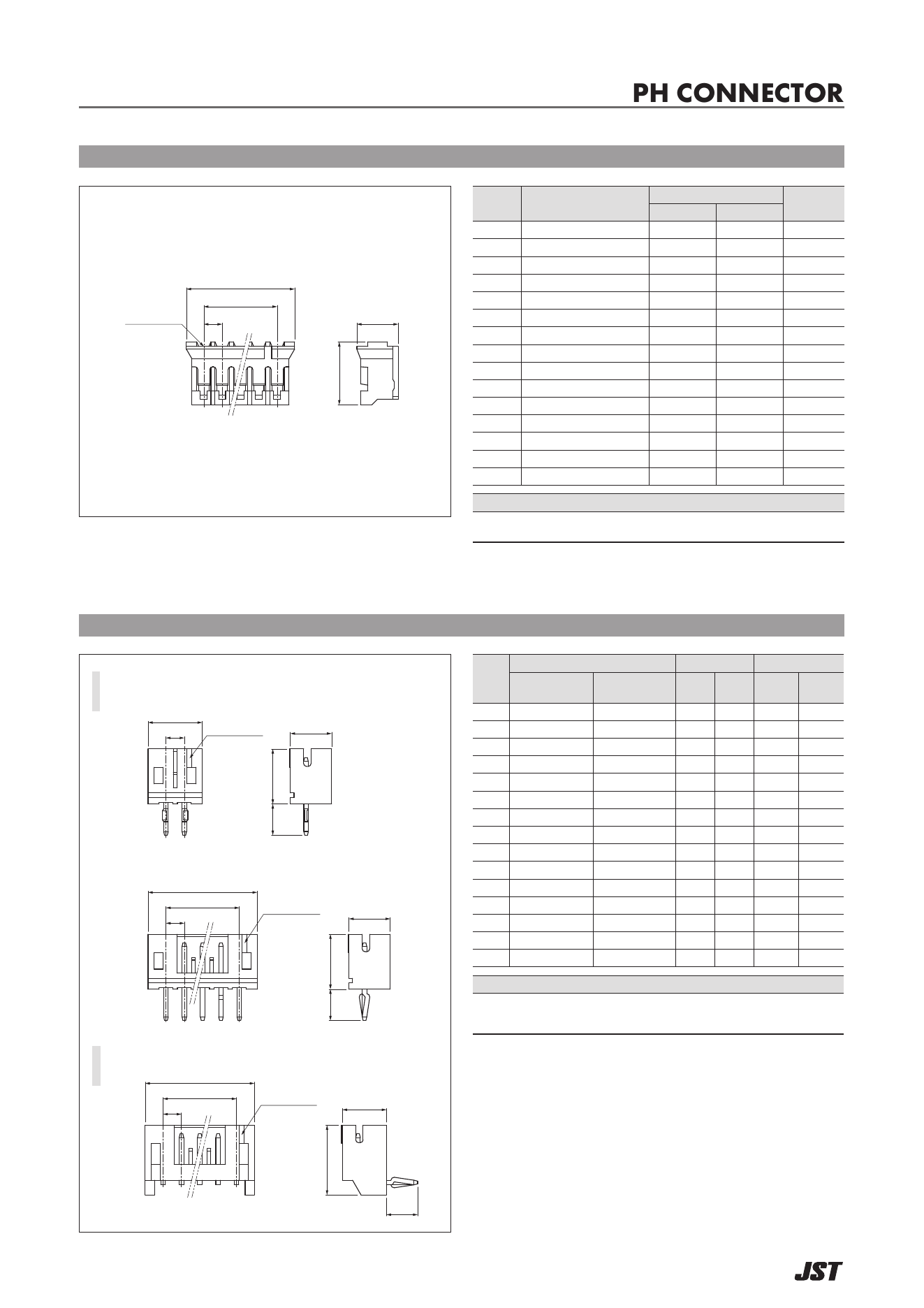
- The 2-circuit top-entry header row of the page 3 table gives A = 2.0 mm and B = 5.9 mm (body length); the drawing shows a 4.5 mm deep body standing 6 mm above the board with (3.4) mm pin tails. Page 1 quotes an 8 mm mounting height, which is the mated header-plus-PHR-housing height shown as (8) in the assembly layout. Applicable board thickness is 0.8–1.6 mm. Confirm the complete land pattern against the released KiCad footprint before fabrication.
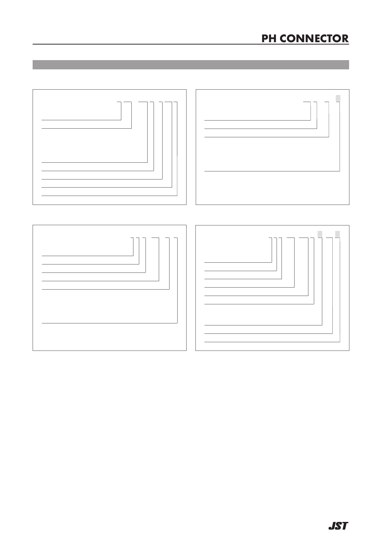
- JST’s 2-circuit top-entry table identifies this exact part as
B2B-PH-K-S; the post is copper alloy with tin plating and the base is natural-white PA resin. - Contacts are passive connector pins. The datasheet does not assign a universal electrical polarity to circuit 1 or circuit 2; map the harness pinout deliberately in the product design.
CAD and integration
- The record’s KiCad footprint is
Connector_JST:JST_PH_B2B-PH-K_1x02_P2.00mm_Vertical, with pads 1 and 2 as through-hole contacts on the 2.00 mm pitch. - The Zener module exposes the callable IO names
PIN_1andPIN_2, mapped to the KiCad symbol pinsPin_1andPin_2. - Do not substitute a side-entry
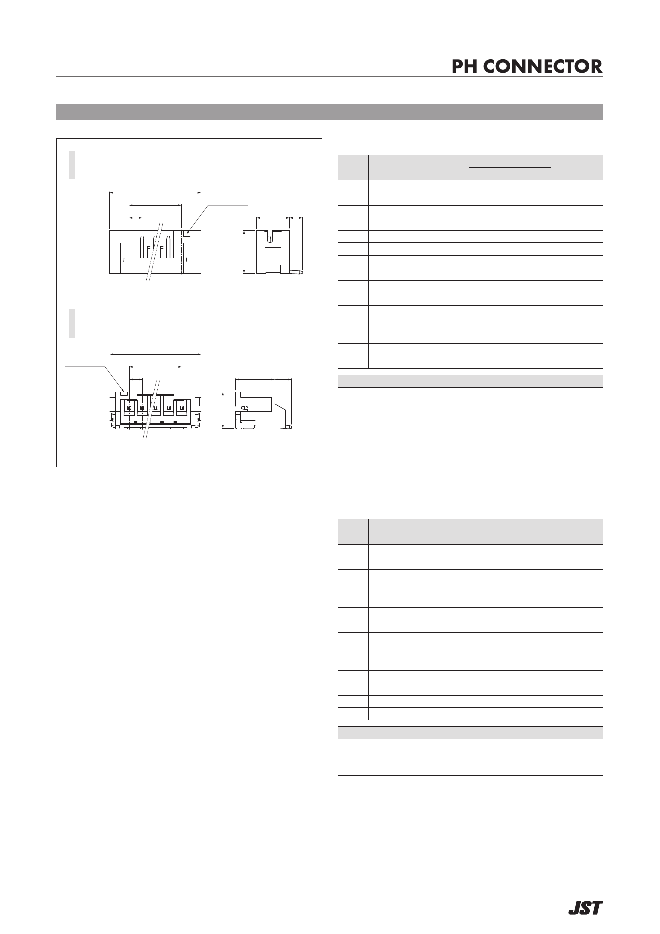
S2Bpart or the SMTSM4-TBfamily when the board placement requires this top-entry through-hole package.
Sources
Figures and diagrams from the PDF
Preview the extracted datasheet assets and open any image in a separate tab for closer inspection.
Use this datasheet from any agent
Send the page, markdown, chunks, or search endpoint to ChatGPT, Claude, embedr-app, or your own tooling.